ST X-NUCLEO-SRC1M1 User manual

Introduction
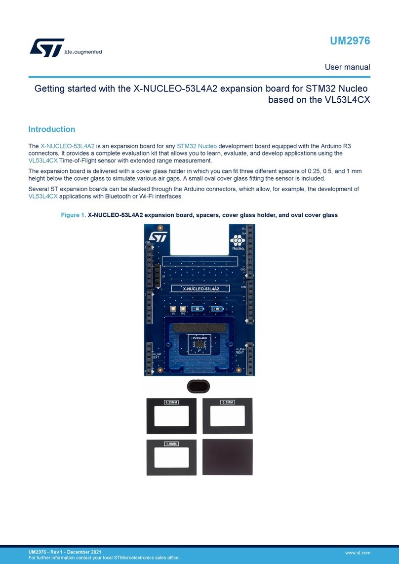
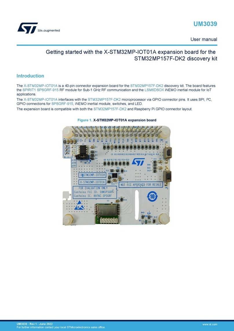
The X-NUCLEO-SRC1M1 expansion board allows evaluating the features of TCPP02-M18 for the USB Type-C™ and the
protections for VBUS and CC lines suitable for source applications.
The expansion board is designed to be stacked on top of any STM32 Nucleo-64 development board with Power Delivery
(UCPD) peripheral embedded in their microcontrollers.
You can also stack it on top of any other STM32 Nucleo-64 development board not supporting the UCPD peripheral for 5
V, source only, to demonstrate the USB Type-C™ basic operations (attach, detach and 5 V power supply current capability
information).
When using an STM32 Nucleo-64 development board with Power Delivery peripheral, data functionalities as a host device or
dual role data (DRD) are also allowed.
The X-NUCLEO-SRC1M1 provides an effective demonstration of the source operation of the USB Type-C™ connector when
an external compatible source is connected to the board. The integrated ST715PU33R LDO linear regulator can supply the
connected STM32 Nucleo development board.
The X-NUCLEO-SRC1M1 is compliant with the latest USB Type-C™ and Power Delivery specifications.
The companion software package (X-CUBE-TCPP) contains the application examples for the development boards embedding
UCPD-based microcontrollers (for example, NUCLEO-G071RB, NUCLEO-G474RE, and NUCLEO-G0B1RE) and for those not
supporting the UCPD peripheral (NUCLEO-L412RB-P).
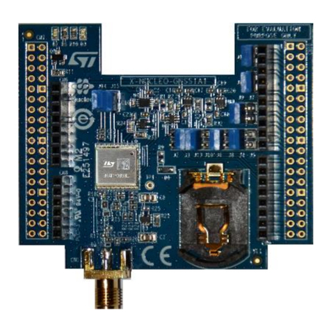
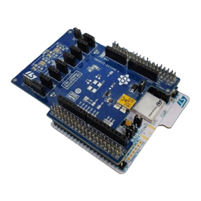
Figure 1. X-NUCLEO-SRC1M1 expansion board
Getting started with the X-NUCLEO-SRC1M1 USB Type-C™ Power Delivery
source expansion board based on TCPP02-M18 for STM32 Nucleo
UM2973
User manual
UM2973 - Rev 1 - December 2021
For further information contact your local STMicroelectronics sales office. www.st.com

1Getting started
1.1 Overview
The X-NUCLEO-SRC1M1 expansion board features:
• Supports all USB Type-C™ Power Delivery SPR profiles up to 100 W
• Manage source role data/power configuration
• Compliant with USB 2.0 dual role data according to STM32 USB data capability
• 8/20 μs surges and overcurrent protections, and discharge for VBUS
• Short to VBUS protection for configuration channel pins (CC1 and CC2)
• ESD protection (IEC61000-4-2 level 4 ± 8 kV contact discharge) for CC1, CC2, D+, and D-
• Overvoltage and overcurrent protections, and discharge for VCONN
• Common mode filter on D+/D- data lines
• Two power modes to optimize the current consumption
• Compliant with programmable power supplies (PPS)
• Free comprehensive development firmware library
• Compliant with STM32 Nucleo-64 boards featuring an STM32 with UCPD feature for Power Delivery and
without UCPD feature for a 5 V solution only
The X-NUCLEO-SRC1M1 provides an interface among three major blocks for the USB Type-C™ Power Delivery
source:
• USB Type-C™ connector;
• the Power Delivery controller embedded in the STM32 (UCPD) on the STM32 Nucleo development board;
• the power supply.
It also provides USB 2.0 data lines interface connection to the STM32 Nucleo MCU.
The BoM is optimized without compromising the protections for:
• VBUS line: overcurrent and surge protections;
• CC lines: overvoltage, overcurrent, and ESD protections;
• data lines: ESD protection and EMI filtering.
As required by the Power Delivery protocol, the TCPP02-M18 features:
• CC lines switch matrix for VCONN;
• VBUS discharge;
• VCONN discharge.
Fault mode report and two optimized power modes are also available.
All these features are managed through I²C communication.
The VBUS current analog readout is also possible when the STM32 ADC is connected to the TCPP02-M18
differential amplifier output.
The following hardware configurations are possible depending on the STM32 UCPD peripheral:
UM2973
Getting started
UM2973 - Rev 1 page 2/25

• the STM32 embeds the UCDP peripheral: 5 V to 20 V PD source or PPS source can be connected to the
provider path
Figure 2. Block diagram of X-NUCLEO-SRC1M1 connected to the STM32 Nucleo with UCPD
Firmware
I2C
USB Type-C™
VBUS
Provider path N-MOSFET
Configuration channels
USB 2.0 Data lines
Protections
STM32 Nucleo development board
ADC
X-NUCLEO-SRC1M1 expansion board
TCPP02-M18
UCPD
STM32
connector
Power bus
CC1/CC2 lines
D+/D-lines
USB 2.0
• the STM32 does not embed the UCPD peripheral: 5 V source only can be connected to the provider path
Figure 3. Block diagram of X-NUCLEO-SRC1M1 connected to the STM32 Nucleo without UCPD
STM32
Firmware
I2C
USB Type-C™
BUS
Power bus
Provider path N-MOSFET
Configuration channels
USB 2.0 Data lines
Protections
STM32 Nucleo development board
ADC
X-NUCLEO-SRC1M1 expansion board
TCPP02-M18
connector
V
CC1/CC2 lines
D+/D- lines
Note: In both the figures above, the solid lines indicate the USB Type-C™ connector connections, whereas the dotted
lines indicate internal connections.
1.2 Hardware architecture
The X-NUCLEO-SRC1M1 expansion board can be used with any STM32 Nucleo-64 development board.
The expansion board must be plugged on the matching pins of the development board CN7 and CN10 ST
morpho connectors.
Two hardware configurations are possible depending on the STM32 UCPD peripheral:
• if the STM32 embeds a UCDP peripheral, connect JP2 and JP3 jumpers to CC1_UCPD and CC2_UCPD,
respectively;
UM2973
Hardware architecture
UM2973 - Rev 1 page 3/25

• if the STM32 does not embed a UCPD peripheral, connect JP2 and JP3 jumpers to CC1_noUCPD and
CC2_noUCPD, respectively.
When plugged onto an STM32 Nucleo development board, the expansion board can be supplied in two different
ways:
• through the STM32 Nucleo ST-LINK supply by using the development board internal LDO;
• through the CN3 screw connector and thanks to the integrated ST715PU33R LDO linear regulator (U2) that
supplies the entire system.
Figure 4. X-NUCLEO-SRC1M1 main functional blocks (top view)
1 and 2: Morpho connectors
3, 4, 5, and 6: Arduino connectors
7: USB Type-C™ connector (CN1)
8: Provider path screw connector (CN3) + LED
9: Jumpers for CC lines configuration (JP2 and JP3)
10: 3.3 V LED
11: Jumpers for the board self-power (LDO out + NRST)
12: TCPP02-M18 USB Type-C™ source protection
13: ECMF02-2AMX6 common mode filter + ESD protection
14: ESDA25P35-1U1M TVS diode
12
3
4
5
6
7
8
9
11
12
14
10
13
UM2973
Hardware architecture
UM2973 - Rev 1 page 4/25

Figure 5. X-NUCLEO-SRC1M1 main functional blocks (bottom view)
1 and 2: Morpho connectors
3, 4, 5, and 6: Arduino connectors
7: 5 V only current capability table
8: STL40DN3LLH5 automotive-grade dual N-channel 30 V, 0.016 mΩ, 11 A STripFET H5 power MOSFET
9: Current sense 7 mΩ shunt resistor
10: ST715PU33R high input voltage LDO linear voltage regulator
2
3
4
5
6
7
8
9
10
1
1.2.1 USB Type-C™ connector
The USB Type-C™ receptacle (CN1) gathers the VBUS path and the main connections, such as CC lines and
USB 2.0 data lines (DP, DM), before dispatching data to the major functional blocks.
UM2973
Hardware architecture
UM2973 - Rev 1 page 5/25

Figure 6. USB Type-C™ receptacle (CN1) and ESDA25P35-1U1M TVS diode (D1)
C13
2.2uF 50V
GND
D1
ESDA25P35-1U1M
TP2
SH22
VBUS
GND
GND
TP5
TP3
C1
330pF 50V
CN1
ConUSB31_632723300011_recept
CC1
A5
Dn1
A7
Dp1
A6
GND1
GND1
GND2
GND2
GND3
A1
GND5
A12
GND6
B12
SBU1
A8
SHELL1
SHELL1
SHELL2
SHELL2
SHELL3
SHELL3
SHELL4
SHELL4
SHELL5
SHELL5
SHELL6
SHELL6
SSRXn1
B10
SSRXn2
A10
SSRXp1
B11
SSRXp2
A11
SSTXn1
A3
SSTXp1
A2
VBUS1
A4
VBUS2
A9
VBUS4
B9
Dn2
B7
Dp2
B6
GND4
B1
SBU2
B8
SSTXn2
B3
SSTXp2
B2
VBUS3
B4
CC2
B5
TP4
C2
330pF 50V
TP1
CC1c
CC2c
An ESDA25P35-1U1M TVS diode (D1) protects the VBUS power line and, consequently, the entire system against
electrical overstress (EOS) when you connect a sink through the USB Type-C™ cable.
To be compliant with the USB Power Delivery standard requirements, the board embeds the 330 pF C1 and C2
capacitors, as well as the 2.2 µF C13 capacitor, which ensures a good system robustness.
1.2.2 USB 2.0 data path and configuration settings
The X-NUCLEO-SRC1M1 expansion board allows the STM32 Nucleo development boards that feature a USB 2.0
peripheral to expose the D+/D- lines on the USB Type-C™ receptacle (CN1).
Most STM32 Nucleo-64 development boards feature this functionality on the CN10-12 and CN10-14 pins of
the ST morpho connectors. The NUCLEO-L412RB-P, NUCLEO-L433RC-P, NUCLEO-L452RE-P and NUCLEO-
L476RG development boards, instead, map USB 2.0 data on CN10-33 and CN10-17 pins.
Two couples of resistances are connected to the ECMF02-2AMX6 (U3) USB 2.0 data line protection to extend the
use of this peripheral to all the STM32 Nucleo-64 development boards.
Figure 7. USB2.0 data line protection ECMF02-2AMX6 (U3) and resistor setup
GND
DP_G4
DP_XX
DM_G4
CC1_G4
ESD
ESD ESD
ESD
D-
GND
D-
D+D+
NC
R19 0
SH13
SH11
R20 0
SH22
D+ecmf
D-ecmf
90 ohms
ZDiff 90 ohms
ZDiff
ECMF02-2AMX6
U3
DM_xx
DP_xx
UM2973
Hardware architecture
UM2973 - Rev 1 page 6/25

By default, the X-NUCLEO-SRC1M1 expansion board mounts R19 and R20 resistors fitted to guarantee USB
2.0 compatibility with all the main microcontroller families. However, for the L4 family (NUCLEO-L412RB-P,
NUCLEO-L433RC-P, NUCLEO-L452RE-P, and NUCLEO-L476RG), you have to remove and replace them with
SH11 and SH13 solder bridges.
D+/- lines are used as data lines (the SH22 solder bridge is opened by default). Short them for source only by
closing the SH22 solder bridge except for 5 V, 0.5 A source in order to ensure compatibility with the USB BC 1.2
standard.
1.2.3 ST morpho and Arduino UNO V3 connectors
The figure below shows the ST morpho and Arduino UNO V3 connectors of the X-NUCLEO-SRC1M1 expansion
board. It details the main connections, functions, and configuration settings.
Figure 8. ST morpho and Arduino UNO V3 connectors
3.3V
GND
GND
GND
5 V
I2C1_SCL
I2C1_SDA
NRST CC1_G4 DP_G4
DM_G4
ADC_Vbusc
ADC_Prov
CC1_G0
ADC_Isense
DP_XX
CC1
CC2
CC1-5V
CC2-5V
ENABLE
FLGN
CN5
SSQ-110-03-F-S
1
2
3
4
5
6
7
8
9
10
CN6
SSQ-108-03-F-S
1
2
3
4
5
6
7
8
R26 0
R31
0
CN10
ESQ-119-14-T-D
2
4
6
8
10
12
14
16
18
20
22
24
26
28
30
32
34
36
38
1
3
5
7
9
11
13
15
17
19
21
23
25
27
29
31
33
35
37
R27 0
R41
100
JP2
JUMPER_3PIN
1
2
3
CN7
ESQ-119-14-T-D
2
4
6
8
10
12
14
16
18
20
22
24
26
28
30
32
34
36
38
1
3
5
7
9
11
13
15
17
19
21
23
25
27
29
31
33
35
37
CN9
SSQ-108-03-F-S
1
2
3
4
5
6
7
8
R24 0
R25 0
R40
100
JP3
JUMPER_3PIN
1
2
3
CN8
SSQ-106-03-G-S
1
2
3
4
5
6
CC2_G0
CC2_G4
CC lines are connected to the UCPD connection of the ST morpho connectors (CN7 CN10).
Two configurations are possible depending on the CC line connection to ST morpho connectors. To release the
STM32 pins, disconnect unused lines by removing R26/R25 or R24/R27.
An STM32 GPIO manages the TCPP02-M18 (U1) ENABLE PIN. You can also connect it directly to 3.3 V.
1.2.4 5 V only current capability
When the STM32 does not embed the UCPD peripheral, it is possible to manage a 5 V only source. JP2 and JP3
are then connected to CC1-5V and CC2-5V, respectively.
Resistor table 1 and table 2 indicate the 5 V current capability:
• R35/R39 mounted (default configuration): 0.5 A max. at 5 V (36 kΩ pullup to 3.3 V);
• R35/R39 not mounted and SH18/SH20 closed: 1.5 A max. at 5 V (12 kΩ pullup to 3.3 V);
• R35/R39 not mounted and SH19/SH21 closed: 3.0 A max. at 5 V (4.7 kΩ pullup to 3.3 V).
UM2973
Hardware architecture
UM2973 - Rev 1 page 7/25

Figure 9. 5 V only current capability
Resistor table 1
3.3V 3.3V
CC1-5V CC2-5V
R34
4.7k
R39
0
R32
36k
SH20 SH21R35
0
SH18
R36
36k
SH19
R37
12k
R33
12k
R38
4.7k
Resistor table 2
When the STM32 embeds the UCPD peripheral, the STM32 manages the 5 V only sources without an external
pullup resistor (JP2 and JP3 are connected to CC1_UCPD and CC2_UCPD, respectively).
1.2.5 I²C bus
An I²C communication is present between the STM32 Nucleo master port and the TCPP02-M18 (U1) slave port
through the SCL and SDA pins.
The TCPP02-M18 I²C default address is 0x68. You can change it to 0x6A by closing the SH16 solder bridge and
unsoldering R28. The high level is then connected to the I2C_ADD pin of the TCPP02-M18.
The X-NUCLEO-SRC1M1 expansion board embeds two 1kΩ I²C pullup resistors (R11 and R12).
1.2.6 Connection of the voltage/current analog senses to the STM32 ADC
The X-NUCLEO-SRC1M1 has two voltage senses connected to the STM32 ADC:
• ADC_VBUSc: measures the VBUS voltage
Note: It is mandatory to ensure the system operation (for example, vSafe0V measurement).
• ADC_Prov: for information on the provider path voltage.
Voltage dividers (ratio 6) are compatible with 24 V DC voltages.
Figure 10. VBUS voltage sense for the STM32 ADC
ADC_VBUSc
R8
200k
R9
40.2k
The X-NUCLEO-SRC1M1 presents the analog current sense output of the TCPP02-M18 (IANA pin) and connects
it to the STM32 ADC (ADC_Isense).
The TCPP02-M18 has an internal differential amplifier (42 V/V) that measures the current flowing through R5 (7
mΩ).
The capacitor footprints (C9 and C11) have been added for potential filtering on analog senses.
UM2973
Hardware architecture
UM2973 - Rev 1 page 8/25

1.2.7 Consumer and provider path
The provider path can be connected to VBUS thanks to two dual STL40DN3LLH5 N-MOSFETs (Q2) controlled by
the TCPP02-M18 gate driver (SRC and GATE pins).
Figure 11. Provider path
Provider
GND
SOURCE
R22
4k
D7
LED5 blue
GND
GND
GND
ADC_Prov
SOURCE
FLGN
D9
NM
R10
47K
R3
200k
C8
NM
Q2B
D5
G
4
3S
R4
40.2k
R5
0.007
GATE 6
SRC 7
ISENSE
9
VBUSc
8
C9
NM
Q2A
STL40DN3LLH5
D
7
G
2
1
S
CN3
1725656
1
2
Isense
The blue LED (D7) signals the voltage presence on the provider path. This LED does not indicate the N-MOSFET
state. In fact, the source LED D7 can be on to indicate the voltage presence on the provider path but, at the same
time, Q2 can be off (no connection of the provider path on the VBUS).
The CN3 screw connector allows accessing the consumer path. You can add additional protections (transient
or free-wheel diodes) on the D9 footprint that is compatible with the ESDAP series (ESDA7P120-1U1M up to
ESDA25P35-1U1M).
The output current of the TCPP02-M18 gate driver charge pump manages the inrush current. It is associated with
the STL40DN3LLH5 drain to the gate MOSFET capacitance (also called Miller capacitance or reverse transfer
capacitance). This association avoids any potential parasitic OCP triggering due to the inrush current generated
by cSnkBulk (between 1 µF and 10 µF), as defined by the USB Power Delivery standard at attach.
When using another MOSFET reference, the C8 external capacitor can be implemented to another MOS
reference. This implementation avoids the OCP triggering due to the inrush current, in case the drain-to-gate
capacitance is too low. The effective drain-to-gate capacitance including C8 must be higher than 20 pF.
When using a higher cSnkBulk capacitance, close Q2 slower. Then, mount the C8 capacitor, choosing 100 pF for
every additional 10 µF on the cSnkBulk terminal.
1.2.8 Overcurrent protection for VBUS and CC lines
The R5 terminal voltage (voltage between the TCPP02-M18 VBUSc and ISENSE pins) protects the TCPP02-M18
from overcurrent on the VBUS. When this voltage is higher than 0.042 V, the overcurrent protection turns on and
opens the provider path.
Table 1. VBUS currents according to the R5 shunt resistor values
Max. nominal current Overcurrent protection threshold R5 shunt resistor
0.5 A 0.9 A 47 mΩ
1.5 A 1.9 A 22 mΩ
3.0 A 4.2 A 10 mΩ
5.0 A 6.0 A 7 mΩ (default value)
When the overcurrent fault is detected:
• FLGN falls;
• the register 2 is updated;
UM2973
Hardware architecture
UM2973 - Rev 1 page 9/25

• the recovery word is mandatory to get back to an operational system. Recovery words are:
– 0x18 written on the I2C register 0 to return to the normal mode;
– 0x28 written on the I2C register 0 to return to the low-power mode;
– 0x08 written on I2C register 0 to return to the hibernate mode.
The recovery word erases the error register (register 2) but does not connect the consumer or the provider path to
VBUS nor VCONN. Write the corresponding bits to close one or more switches on the additional step.
1.2.9 CC line overvoltage protection
Unplugging a defective cable, with a voltage higher than 5 V, from the USB Type-C™ connector might cause
a VBUS short to the CC lines (adjacent lines). This also might apply a voltage higher than the one specified for
the STM32 AMR on the CC lines (FT IO). The TCPP02-M18 overvoltage protection on the CC lines protects the
STM32.
1.2.10 LDO
The ST715PU33R (U2) is a 3.3 V high input voltage LDO, supplied through the provider path (for example, CN3).
To supply the system with the LDO output, you must close JP1 with:
• a jumper between 1 and 2 to connect the 3.3 V output voltage to the 3.3 V of the system;
• a jumper between 3 and 4 to force the STM32 NRST pin to 3.3 V (otherwise it might cause a potential
parasitic reset).
The D6 green LED signals the 3.3 V presence on the X-NUCLEO-SRC1M1.
Figure 12. LDO configuration
3. 3 V
High input voltage
85 mA LDO linear regulator
GND GND
3.3V
NRST
U2ST715PU33R
IN
1
9
Exp Pad GND
OUT 8
NC1
2
NC2
3
GND
4
NC3 7
NC4 6
FB 5
JP1
TSW-102-07-F-D
1 2
3 4
R23
1k
D8
LED green
C6
470n 5V
1
2
C5
100n 25V 1
2
Provider
GND
SOURCE
R22
4k
D7
LED5 blue
1.2.11 TCPP02-M18 overview
3.3 V is connected to the VCC/VCONN pin of the TCPP02-M18 (U1). It supplies the IC and also provides the
input voltage for VCONN.
VCONN voltage can be in the range of 3.0 to 5.5 V according to the USB-PD standard: VCC/VCONN is compatible
with this voltage range.
All TCPP02-M18 I/Os connected to the STM32 are compliant with 3.3 V and 1.8 V (FLGn, ENABLE, IANA, SDA,
SLC), except CC1 and CC2 I/Os, in which they are in accordance with the USB-PD standard voltages. I2C_ADD
is also compliant with 3.3 V and 1.8 V.
The TCPP02-M18 ENABLE pin is connected to the STM32 GPIO but you can also connect it directly to 3.3 V with
the R29 resistor.
The CBIAS pin capacitor (C3) is the TCPP02-M18 ESD capacitor. Its value must be ≥100 nF and 50 V rated to
limit the voltage derating.
UM2973
Hardware architecture
UM2973 - Rev 1 page 10/25
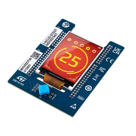
Figure 13. TCPP02-M18
3. 3 V
High input voltage
85 mA LDO linear regulator
GND GND
3.3V
NRST
U2ST715PU33R
IN
1
9
Exp Pad GND
OUT 8
NC1
2
NC2
3
GND
4
NC3 7
NC4 6
FB 5
JP1
TSW-102-07-F-D
1 2
3 4
R23
1k
D8
LED green
C6
470n 5V
1
2
C5
100n 25V 1
2
Provider
GND
SOURCE
R22
4k
D7
LED5 blue
1.3 STM32 resources
The STM32 resources provided to the TCPP02-M18 are compliant with 1.8 V and 3.3 V. This allows using the 1.8
V of the STM32 with a minor change: decrease the voltage divider resistors (R4 and R9) to 20 k in order to set the
divider ratio to 11.
To start a USB Power Delivery source, the required resources on the STM32 are:
• the UCPD peripheral that manages the USB Power Delivery protocol;
• the I2C bus that can be shared with other slaves;
• the ADC to get the VBUS voltage image.
To optimize the power consumption on the battery-powered system, at cable attach, you have to switch the
TCPP02-M18 from the low-power mode to the normal mode with the I2C request, to ensure a good USB-PD
communication through the CC lines.
Optional resources are:
• a USB 2.0 peripheral;
• an ADC to get the provider path voltage and the current on the VBUS images.
Table 2. STM32 resources coming from the X-NUCLEO-SRC1M1
What USB-PD minimal resources Additional features Comments
UCPD CC1 X USB-PD CC
UCPD CC2 X USB-PD CC
I2C SCL X I2C bus clock
I2C SDA X I2C bus data
GPIO FlLGN X Fault flag
ADC VBUSc X VBUS voltage info
ADC provider X Provider path voltage info
ADC Isense X Current on VBUS for PPS
GPIO ENABLE X VDD via GPIO
USB D+ X USB 2.0 data line
USB D- X USB 2.0 data line
UM2973
STM32 resources
UM2973 - Rev 1 page 11/25

2Demo application setup
The X-NUCLEO-SRC1M1 expansion board flexibility allows demonstrating the TCPP02-M18 protection features
and capabilities with a wide range of STM32 Nucleo development boards.
The X-CUBE-TCPP companion software package contains specific application examples for the STM32 Nucleo
development boards, which embed the USB Type-C™ and Power Delivery management (NUCLEO-G071RB,
NUCLEO-G474RE, and NUCLEO-G0B1RE) or not (NUCLEO-L412RB-P).
2.1 Overview of the application example for STM32G474RE (embedding the UCPD
peripheral)
This example shows how to start a battery-powered source application with the TCPP02-M18 and the
STM32G474RE MCU using an X-NUCLEO-SRC1M1 stacked on a NUCLEO-G474RE.
The example includes two different modes:
1. a programming mode, when the ST-LINK powers the STM32G474RE;
2. a system validation (realistic case) in one of the following cases:
– the source (provider path) powers the STM32G474RE;
– you cannot program the STM32G474RE as the ST-LINK is not supplying the system;
–STM32CubeMonUCPD is still running when the ST-LINK is connected.
These two modes cannot be merged because the 3.3 V coming from ST-LINK manages the STM32 NRST pin. If
the ST-LINK is not powered, the STM32 NRST pin becomes HiZ and might cause parasitic resets.
2.1.1 Programming/debugging example for STM32G747RE
Step 1. Configure the X-NUCLEO-SRC1M1 as follows.
Step 1a. Do not put any jumper on JP1.
Step 1b. Put the JP2 and JP3 jumpers on CC1_UCPD and CC2_UCPD, respectively.
Step 2. Configure the NUCLEO-G474RE as follows:
Step 2a. On JP5, put the 5V_STLINK jumper to select 5 V from the ST-LINK USB as a power source
for the STM32G747RE.
Step 2b. On JP8, put the jumpers on positions 1-2 to select 5 V as a reference voltage initiator.
Step 3. Connect the USB type A to micro-USB cable to the NUCLEO-G474RE.
Step 4. Drag and drop G4_SRC1M1_SRC.bin to the NUCLEO-G474RE node (or choose an IDE for
programming).
Step 5. Monitor with STM32CubeMonUCPD.
2.1.2 STM32G474RE system validation
Step 1. Configure the X-NUCLEO-SRC1M1 as follows.
Step 1a. On JP1, put two jumpers (LDO OUT - 3.3 V and NRS - 3.3 V) to power the STM32G747RE
through the 3.3 V LDO output.
Step 1b. Put the JP2 and JP3 jumpers on CC1_UCPD and CC2_UCPD, respectively.
Step 2. Configure the NUCLEO-G474RE as follows:
Step 2a. Do not put any jumper on JP5.
Step 2b. On JP8, put the jumpers on positions 1-2 to select 5 V as a reference voltage initiator.
Step 3. Connect the USB type A to micro-USB cable to the NUCLEO-G474RE.
Step 4. Monitor with STM32CubeMonUCPD.
UM2973
Demo application setup
UM2973 - Rev 1 page 12/25

2.2 Overview of the application example for STM32L412RB (without UCPD
peripheral), 5 V only
This example shows how to start a battery-powered source application with the TCPP02-M18 and the
STM32L412RB MCU using an X-NUCLEO-SRC1M1 stacked on a NUCLEO-L412RB-P.
The example includes two different modes:
1. a programming mode, when the ST-LINK powers the STM32L412RB;
2. a system validation (realistic case) in one of the following cases:
– the source (provider path) powers the STM32L412RB;
– you cannot program the STM32L412RB as the ST-LINK is not supplying the system;
–STM32CubeMonUCPD is still running when the ST-LINK is connected.
These two modes cannot be merged as the 3.3 V coming from ST-LINK manages the STM32 NRST pin. If the
ST-LINK is not powered, the STM32 NRST pin becomes HiZ and might cause parasitic resets.
2.2.1 Programming/debugging example for STM32L412RB
Step 1. Configure the X-NUCLEO-SRC1M1 as follows.
Step 1a. Do not put any jumper on JP1.
Step 1b. Put the JP2 and JP3 jumpers on CC1_UCPD and CC2_UCPD, respectively.
Step 2. Configure the NUCLEO-L412RB-P as follows:
Step 2a. On JP5, put the 5V_STLINK jumper to select 5 V from the ST-LINK USB as a power source
for the STM32L412RB.
Step 2b. On JP8, put the jumpers on positions 1-2 to select 5 V as a reference voltage initiator.
Step 3. Connect the USB type A to micro-USB cable to the NUCLEO-L412RB-P.
Step 4. Drag and drop G4_SRC1M1_SRC.bin to the NUCLEO-L412RB-P node (or choose an IDE for
programming).
Step 5. Monitor with STM32CubeMonUCPD.
2.2.2 STM32GL412RB system validation
Step 1. Configure the X-NUCLEO-SRC1M1 as follows.
Step 1a. On JP1, put two jumpers (LDO OUT - 3.3 V and NRS - 3.3 V) to power the STM32GL412RB
through the 3.3 V LDO output.
Step 2. Configure the NUCLEO-L412RB-P as follows:
Step 2a. Do not put any jumper on JP5.
Step 2b. On JP8, put the jumpers on positions 2-3 to select 5 V as a reference voltage initiator.
Step 3. Connect the USB type A to micro-USB cable to the NUCLEO-L412RB-P.
Step 4. Monitor with STM32CubeMonUCPD.
UM2973
Overview of the application example for STM32L412RB (without UCPD peripheral), 5 V only
UM2973 - Rev 1 page 13/25

3Schematic diagrams
Figure 14. X-NUCLEO-SRC1M1 circuit schematic (1 of 3)
VBUS
3.3V
GND
GND
GND
GND
GND
GND
GND
GND
GND
GND
GND
3.3V3.3V
CC1
CC2
I2C1_SDA
ENABLE
I2C_ADD
DP_G4
DP_XX
DM_G4
CC1_G4
ADC_Isense
I2C1_SCL
ADC_Prov
SOURCE
ADC_VBUSc
FLGN
D9
NM
TP5
ESD
ESD ESD
ESD
D-
GND
D-
D+D+
NC
R10
47K
R30
0
R19 0
R8
200k
R29
NM
R3
200k
TP3
SH13
C1
330pF 50V
R9
40.2k
C11
NM
C8
NM
CN1
ConUSB31_632723300011_recept
CC1
A5
Dn1
A7
Dp1
A6
GND1
GND1
GND2
GND2
GND3
A1
GND5
A12
GND6
B12
SBU1
A8
SHELL1
SHELL1
SHELL2
SHELL2
SHELL3
SHELL3
SHELL4
SHELL4
SHELL5
SHELL5
SHELL6
SHELL6
SSRXn1
B10
SSRXn2
A10
SSRXp1
B11
SSRXp2
A11
SSTXn1
A3
SSTXp1
A2
VBUS1
A4
VBUS2
A9
VBUS4
B9
Dn2
B7
Dp2
B6
GND4
B1
SBU2
B8
SSTXn2
B3
SSTXp2
B2
VBUS3
B4
CC2
B5
Q2B
D5
G
4
3S
SH11
C3
100n 50V
R4
40.2k
R5
0.007
TP4
D1
ESDA25P35-1U1M
R11
1K
C2
330pF 50V
TP2
R20 0
U1
TCPP02-M18
CBIAS
12
CC1 2
CC1c
13
CC2 4
CC2c
11
ENABLE 1
FLGn 18
GATE 6
SRC 7
GND
10
I2C_ADD 15
IANA 5
ISENSE
9
SCL
17
SDA
16
VBUSc
8
VCC / VCONN 3
GND2
14
exp pad GND
19
C9
NM
TP1
Q2A
STL40DN3LLH5
D
7
G
2
1
S
CN3
1725656
1
2
C13
2.2uF 50V
SH22
R12
1K
Isense
CC1c
CC1c
CC2c
CC2c
D+ecmf
D-ecmf
90 ohms
ZDiff 90 ohms
ZDiff
ECMF02-2AMX6
U3
DM_xx
DP_xx
UM2973 - Rev 1 page 14/25
UM2973
Schematic diagrams

Figure 15. X-NUCLEO-SRC1M1 circuit schematic (2 of 3)
Resistor table 1
3.3V
GND
3.3V
GND
GND
GND
GND
3.3V
5 V
5 V
3.3V 3.3V
GND
I2C1_SDA
I2C1_SCL
I2C1_SDA
NRST CC1_G4 DP_G4
DM_G4
ADC_Vbusc
ADC_Prov
CC1_G0
ADC_Isense
DP_XX
I2C_ADD
CC1
CC2
CC1-5V
CC2-5V
I2C1_SCL
SOURCE
ENABLE
FLGN
CC1-5V CC2-5V
R34
4.7k
R39
0
CN5
SSQ-110-03-F-S
1
2
3
4
5
6
7
8
9
10
SH16
CN6
SSQ-108-03-F-S
1
2
3
4
5
6
7
8
R26 0
R31
0
R32
36k
SH17
CN4
M20-9980446
1 2
3 4
5 6
7 8
SH20
CN10
ESQ-119-14-T-D
2
4
6
8
10
12
14
16
18
20
22
24
26
28
30
32
34
36
38
1
3
5
7
9
11
13
15
17
19
21
23
25
27
29
31
33
35
37
R27 0
R41
100
SH21
JP2
JUMPER_3PIN
1
2
3
R28
1k
R35
0
CN7
ESQ-119-14-T-D
2
4
6
8
10
12
14
16
18
20
22
24
26
28
30
32
34
36
38
1
3
5
7
9
11
13
15
17
19
21
23
25
27
29
31
33
35
37
CN9
SSQ-108-03-F-S
1
2
3
4
5
6
7
8
SH18
R24 0
R36
36k
R25 0
SH19
R37
12k
R40
100
JP3
JUMPER_3PIN
1
2
3
R33
12k
CN8
SSQ-106-03-G-S
1
2
3
4
5
6
R38
4.7k
CC2_G0
CC2_G4
Resistor table 2
UM2973 - Rev 1 page 15/25
UM2973
Schematic diagrams

Figure 16. X-NUCLEO-SRC1M1 circuit schematic (3 of 3)
3. 3 V
High input voltage
85 mA LDO linear regulator
GND GND
3.3V
NRST
U2ST715PU33R
IN
1
9
Exp Pad GND
OUT 8
NC1
2
NC2
3
GND
4
NC3 7
NC4 6
FB 5
JP1
TSW-102-07-F-D
1 2
3 4
R23
1k
D8
LED green
C6
470n 5V
1
2
C5
100n 25V 1
2
Provider
GND
SOURCE
R22
4k
D7
LED5 blue
UM2973 - Rev 1 page 16/25
UM2973
Schematic diagrams

4Bill of materials
Table 3. X-NUCLEO-SRC1M1 bill of materials
Item Q.ty Ref. Part/value Description Manufacturer Order code
1 1 U1
TCPP02-M18
QFN-18L 3.5 x
3.5
USB Type-C™
port protection
for source
application
ST TCPP02-M18
2 1 U3
ECMF02-2AMX
6 QFN-6L
1.7x1.5
Common-mode
filter and ESD
protection for
USB 2.0 and
MIPI/MDDI
interfaces
ST ECMF02-2AMX6
3 1 D1
ESDA25P35-1U
1M QFN-2L
1.6x1.0 25 V
High-power
transient
voltage
suppressor
ST ESDA25P35-1U1M
4 1 Q2
STL40DN3LLH
5 PowerFLAT
5.0x6.0 double
island WF 30 V
Automotive-
grade dual N-
channel 30 V,
0.016 ohm typ.,
11 A STripFET
H5 Power
MOSFET in a
PowerFLAT 5x6
double island
package
ST STL40DN3LLH5
5 1 U2 ST715PU33R
DFN8 3x3 24 V
High input
voltage, 85 mA
LDO linear
regulator
ST ST715PU33R
7 1 CN1 USB_TypeC_R
eceptacle
USB Type-
C™connector
Wurth
Electronics Inc. 632723300011
8 1 CN3
2.54 2-position
screw connector
2x1 2.54 mm
pitch
Through-hole
screw connector
Wurth
Electronics Inc. 691210910002
9 1 CN4
2.54 2x4 jumper
2.54 mm 2x4
male connector
Jumper Wurth
Electronics Inc. 61300821121
10 1 JP1
2.54 2x2 jumper
2.54 2x4 male
connector
Jumper Wurth
Electronics Inc. 61300421121
11 2 JP2 JP3
2.54 3x1 jumper
2.54 1x3 male
connector
Jumpers Wurth
Electronics Inc. 61300311121
12 1 CN5 Arduino UNO
10 pins 2.54 10
Arduino
connector
Wurth
Electronics Inc. 61301011821
13 2 CN6 CN9 Arduino UNO 8
pins 2.54 8
Arduino
connector
Wurth
Electronics Inc. 61300811821
14 1 CN8 Arduino UNO 6
pins 2.54 6
Arduino
connector
Wurth
Electronics Inc. 61300611821
15 2 CN7 CN10
ST morpho
connector strip
19x2p 2.54
Morpho
connector Samtec ESQ-119-24-T-D
UM2973
Bill of materials
UM2973 - Rev 1 page 17/25

Item Q.ty Ref. Part/value Description Manufacturer Order code
16 1 D7 LED SMD 0603 Blue LED Wurth
Electronics Inc. 150060BS75000
17 1 D8 LED SMD 0603 Green LED Wurth
Electronics Inc. 150060GS75020
18 2 C1 C2
330 pF 0402
X7R 50 VDC 50
V ±10%
Multilayer
ceramic
capacitors
Wurth
Electronics Inc. 885012205058
19 1 C3
100 nF 0402
X7R 50 VDC 50
V ±10%
Multilayer
ceramic
capacitor
Wurth
Electronics Inc. 885012205086
20 1 C5
100 nF 0402
X7R 25VDC 25
V ±10%
Multilayer
ceramic
capacitor
Wurth
Electronics Inc. 885012205085
21 1 C6
470 nF 0402
X5C 6 VDC 6 V
±10%
Multilayer
ceramic
capacitor
Wurth
Electronics Inc. 885012105004
22 1 R5 0.007 1206
0.007 ±1% Resistor Panasonic ERJMP2MF7M0U
23 2 R3 R8 200 k 0402 1/16
W ±1% Resistors Any Any
24 2 R4 R9 40.2 k 0402
1/16 W ±1% Resistors Any Any
25 3 R11 R12 R23
R28
1 K 0402 1/16
W ±1% Resistors Any Any
26 1 R22 3.9 k 0402 1/16
W ±1% Resistor Any Any
27 1 R10 47 k 0402 1/16
W ±1% Resistor Any Any
28 10
R19 R20 R24
R25 R26 R27
R30 R31 R35
R39
0 0402 Resistors Any Any
29 1 C13
2.2 µF 0603
X5R 50 VDV 50
V ±10%
Multilayer
ceramic
capacitor
Any Any
30 2 R40 R41 100 0402 1/16
W ±1% Resistors Any Any
31 2 R32 R36 36 k 0402 1/16
W ±1% Resistors Any Any
32 2 R33 R37 12 k 0402 1/16
W ±1% Resistors Any Any
33 2 R34 R38 4.7k 0402 1/16
W ±1% Resistors Any Any
UM2973
Bill of materials
UM2973 - Rev 1 page 18/25

5Board versions
Table 4. X-NUCLEO-SRC1M1 versions
Finished good Schematic diagrams Bill of materials
XNUCLEO$SRC1M1A (1) XNUCLEO$SRC1M1A schematic diagrams XNUCLEO$RSC1M1A bill of materials
1. This code identifies the X-NUCLEO-SRC1M1 evaluation board first version.
UM2973
Board versions
UM2973 - Rev 1 page 19/25

6Regulatory compliance information
Formal Notice Required by the U.S. Federal Communications Commission
FCC NOTICE:
This kit is designed to allow:
(1) Product developers to evaluate electronic components, circuitry, or software associated with the kit to
determine
whether to incorporate such items in a finished product and
(2) Software developers to write software applications for use with the end product.
This kit is not a finished product and when assembled may not be resold or otherwise marketed unless all
required FCC equipment authorizations are first obtained. Operation is subject to the condition that this product
not cause harmful interference to licensed radio stations and that this product accept harmful interference. Unless
the assembled kit is designed to operate under part 15, part 18 or part 95 of this chapter, the operator of the kit
must operate under the authority of an FCC license holder or must secure an experimental authorization under
part 5 of this chapter 3.1.2.
The evaluation kit has been designed to comply with part 15 of the FCC Technical Rules. Operation is subject to
the following two conditions: (1) This device may not cause harmful interference, and (2) this device must accept
any interference received, including interference that may cause undesired operation.
This equipment has been tested and found to comply with the limits for a Class B digital device, pursuant to part
15 of the FCC Rules. These limits are designed to provide reasonable protection against harmful interference
in a residential installation. This equipment generates, uses and can radiate radio frequency energy and, if not
installed and used in accordance with the instructions, may cause harmful interference to radio communications.
However, there is no guarantee that interference will not occur in a particular installation.
Standard applied: FCC CFR 47 Part 15 Subpart B. Test method applied: ANSI C63.4 (2014).
Formal Product Notice Required by Industry Canada Innovation, Science and Economic Development
Canada compliance:
For evaluation purposes only. This kit generates, uses, and can radiate radio frequency energy and has not been
tested for compliance with the limits of computing devices pursuant to Industry Canada (IC) rules.
À des fins d'évaluation uniquement. Ce kit génère, utilise et peut émettre de l'énergie radiofréquence et n'a pas
été testé pour sa conformité aux limites des appareils informatiques conformément aux règles d'Industrie Canada
(IC).
This device has been tested with Innovation, Science and Economic Development RSS standards. Operation is
subject to the following two conditions: (1) this device may not cause harmful interference, and (2) this device
must accept any interference received, including interference that may cause undesired operation.
Standard applied: ICES-003 Issue 7 (2020), Class B. Test method applied: ANSI C63.4 (2014).
Cet appareil a été testé pour les normes RSS d'Innovation, Science et Développement économique. L'utilisation
est soumise aux deux conditions suivantes: (1) cet appareil ne doit pas causer d'interférences nuisibles, et (2)
cet appareil doit accepter de recevoir tous les types d’interférence, y comprises les interférences susceptibles
d'entraîner un fonctionnement indésirable.
Norme appliquée: NMB-003, 7e édition (2020), Classe B. Méthode d'essai appliquée: ANSI C63.4 (2014).
Formal product notice required by EU
This device is in conformity with the essential requirements of the Directive 2014/30/EU (EMC) and of the
Directive 2015/863/EU (RoHS).
Standards applied (Class B): EN 61000-6-1:2019, EN 61000-6-3:2021, EN 55032:2015 + A1:2020, EN
55035:2017 + A11:2020, EN 61000-3-2:2019, EN 61000-3-3:2013 + A1:2019
UM2973
Regulatory compliance information
UM2973 - Rev 1 page 20/25
Table of contents
Other ST Computer Hardware manuals

ST
ST STM32F4 Series User manual

ST
ST X-CUBE-CELLULAR User manual

ST
ST STDES-65ACFADP Specification sheet

ST
ST STM32U5 User manual

ST
ST MotionTL User manual

ST
ST X-NUCLEO-OUT15A1 User manual

ST
ST X-NUCLEO-GFX01M1 User manual

ST
ST 32L152CDISCOVERY User manual

ST
ST X-NUCLEO-S2868A2 User manual

ST
ST STEVAL-USBI2CFT User manual

ST
ST STM32F411 User manual

ST
ST STM32U5 Nucleo-64 User manual

ST
ST X-NUCLEO-IOD02A1 User manual

ST
ST STEVAL-IFS013V2 User manual

ST
ST X-NUCLEO-53L3A2 User manual

ST
ST STM32CubeF2 User manual

ST
ST AN5717 Installation and operating instructions

ST
ST STM32 Nucleo User manual

ST
ST STA309A User manual

ST
ST STM32F3DISCOVERY User manual