ST X-NUCLEO-IOD02A1 User manual

Introduction
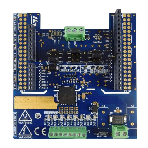
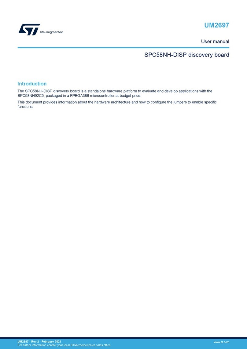
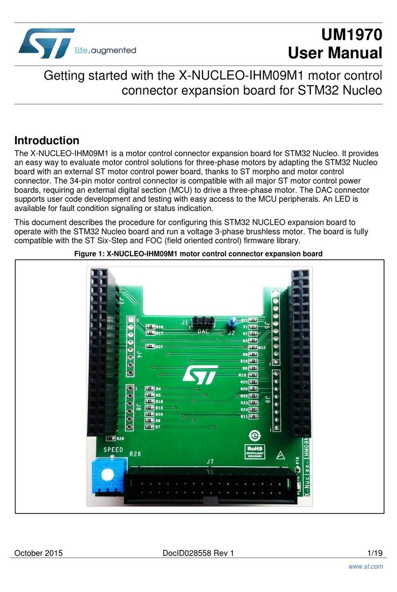
The X-NUCLEO-IOD02A1 expansion board for STM32 Nucleo is based on the L6364Q dual channel SIO and IO-Link PHY
device transceiver embedding 50 mA 3.3 V and 5.0 V voltage regulators, DC-DC converter and M-sequence management.
The expansion board provides an affordable and easy-to-use solution for the development of SIO and IO-Link industrial sensor
applications, letting you easily evaluate the L6364Q communication features and robustness.
The X-NUCLEO-IOD02A1 communicates with the STM32 controller via SPI and GPIO pins and it is compatible with the Arduino
UNO R3 (default configuration) and ST morpho (optional, not mounted) connectors (when connected to a NUCLEO-L073RZ or
NUCLEO-G071RB development board).
Communication via IO-Link can be performed in either Multi-byte and Single-byte modes with SPI control of IC configuration and
bidirectional sensor data transmission, or in Transparent mode with SPI control of IC configuration and UART interfacing for
bidirectional sensor data transmission.
The switches on the X-NUCLEO-IOD02A1 conveniently allow you to configure L6364Q and expansion board settings such as
transmission mode and DC-DC converter enable/disable according to application requirements.
You can also perform evaluation of comprehensive industrial sensor modules by connecting the X-NUCLEO-IOD02A1 to the X-
NUCLEO-IKS02A1 sensor shield.
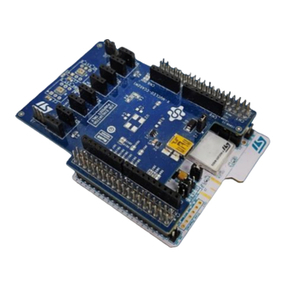
Figure 1. X-NUCLEO-IOD02A1 expansion board
Getting started with the dual channel IO-Link device expansion board for STM32
Nucleo
UM2741
User manual
UM2741 - Rev 1 - September 2020
For further information contact your local STMicroelectronics sales office.
www.st.com

1Getting started
1.1 Overview
The X-NUCLEO-IOD02A1 SIO and IO-Link device board, embedding the L6364Q intelligent dual channel IO-Link
transceiver, is designed to meet the electrical and communication protocol requirements with the IO-Link master.
The expansion board main features are:
• Based on the L6364Q IO-Link device dual transceiver in QFN package with the following main
characteristics:
– 2-channel (CQ and DIO) IO-Link PHY layer
– IO-Link DLL (M-sequence handler and checksum)
– Wake-up detection
– Interrupt diagnostic pin
– SPI and UART interfaces
– 50 mA 3.3 V and 5.0 V linear regulators
– 50 mA adjustable (5.0 ÷ 10.8 V) buck converter
– Overload protection with adjustable intervention threshold
– Overheating protection with adjustable shutdown threshold
– Full reverse polarity on process side
– Ground and VCC wire break protections
– QFN-20L (4 x 4 x 0.9 mm) package
• 5 to 35 V operating voltage range
• Red LED and green LED for status diagnostics
• Radiated Emissions (EM Fields 30 MHz-1 GHz) < 40dB µV/m
• Immunity to conducted disturbance (150 kHz-80 MHz) ≤ 10 V
• Immunity to RF EM Fields (80 MHz-1 GHz) ≤ 10 V/m
• Immunity to RF EM Fields (1 GHz-2.7 GHz) ≤ 3 V/m
• Immunity to SURGE pulse (500 Ohm coupling) ≤ ± 1.2 kV
• Immunity to ESD contact/air ≤ ±3 kV
• Immunity to BURST noise ≤ ±1 kV
• Compatible with STM32 Nucleo development boards
• Equipped with Arduino UNO R3 connectors
• RoHS and WEEE compliant
Important:
The L6364Q is designed for full compliance with EMC immunity levels required by IEC 61131-9 (and IEC 60947-5-2 for surge
pulse). The X-NUCLEO-IOD02A1 expansion board, however, is intended for development purposes and the long net paths
along the Arduino connectors may impact ESD and Burst immunity levels.
1.1.1 Digital section
The digital section consists of the STM32 interface and the digital supply voltages to and from the STM32 Nucleo
development board and the X-NUCLEO-IOD02A1 expansion board via four Arduino UNO R3 connectors.
The on-board L1 inductor and C6 capacitor enable the step-down converter (active by default through SW4 by
closing 1-2) embedded in the L6364Q. The converter also supplies the two L6364Q internal LDOs to reduce
power dissipation, whose output voltage can supply the STM32 Nucleo development board via the Vin net through
JP8 (closed) and CN6.
To supply your development board through an L6364Q LDO:
• set JP5 to E5V for the NUCLEO-L053R8 or NUCLEO-L073RZ development board
• close JP2 between pins 2-3 instead of 1-2 for the NUCLEO-G071RB development board
The digital signal levels are set by the MCU on the STM32 Nucleo development board, so the L6364Q VDIG pin
is connected by SW2 to the proper voltage rail (3.3 V or 5.0 V from CN6).
UM2741
Getting started
UM2741 - Rev 1 page 2/14
To alternatively supply the STM32 Nucleo development boards independently via USB:
•close JP5 to U5V on NUCLEO-L053R8 or NUCLEO-L073RZ development board
• close JP2 pins 1-2 on NUCLEO-G071RB) and ensure J8 is left open
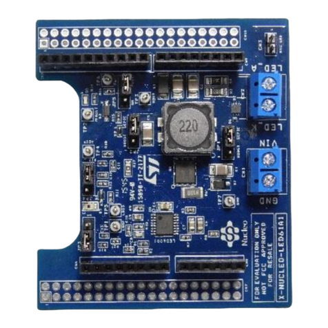
Figure 2. X-NUCLEO-IOD02A1 expansion board
dotted line indicates the digital interface section
The four Arduino UNO R3 connectors also allow the expansion board to communicate with the STM32 Nucleo
development board via the following STM32 peripheral and GPIO resources:
•SPI (CN5, CN8): control interface allowing communication between the MCU (SPI master) and the L6364Q
(SPI slave) to configure the internal L6364Q register or read the status registers. In Single-Byte and Multi-
Byte Communication Modes, the SPI is also used for the data transfer to and from the sensor.
• INT (CN9): interrupt line driven by the L6364Q to alert the MCU of a new event. The MCU reads the status
register of the L6364Q via the SPI interface to determine which event occurred.
• UART TX (CN5), UART RX (CN9): interface for sensor data transfer via CQ line used by the MCU in
Transparent Communication Mode. When this mode is selected, JP4 and JP5 jumpers must be closed.
• CTLD (CN8): the L6364Q provides the DIO as a secondary digital input/output pin. In DIO Mode, this pin can
be controlled by SPI (similar to CQ) or in direct mode by CTLD pin (J9 must be closed).
1.1.2 Power section
The power section (CN1, CN2, CN3) includes the power supply voltage (L+, L-), the transmission lines (CQ, DIO),
the output voltage of the step-down converter (VDCDC) and the additional supply rail (DOUT), which is protected
against reverse polarity by the diode embedded in the L6364Q.
CN1 and CN2 are usually connected to the corresponding pins of an IO-Link Master (e.g. P-NUCLEO-IOM01M1)
that controls communication and supplies the X-NUCLEO-IOD02A1 via the L+ rail. The CQ line is used to
exchanged data between IO-Link Master and IO-Link Device. The DIO line is the additional digital channel
typically used in the port class A (type A). L- is the electrical ground reference between the two systems.
CN3 is an additional connector allowing further connections, such as for actuators.
UM2741
Overview
UM2741 - Rev 1 page 3/14

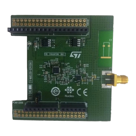
Figure 3. X-NUCLEO-IOD02A1 expansion board
dotted line indicates the power section
1.2 Hardware requirements
The X-NUCLEO-IOD02A1 expansion board is designed to be used with the NUCLEO-L053R8, NUCLEO-L073RZ
or NUCLEO-G071RBSTM32 Nucleo development boards.
To function correctly, the X-NUCLEO-IOD02A1 must be plugged onto the matching Arduino UNO R3 connector
pins on the STM32 Nucleo board as shown below.
Figure 4. X-NUCLEO-IOD02A1 and STM32 Nucleo stack
UM2741
Hardware requirements
UM2741 - Rev 1 page 4/14

1.3 System requirements
To use the STM32 Nucleo development boards with the X-NUCLEO-IOD02A1 expansion board, you need:
•a Windows PC/laptop (Windows 7 or above)
• a type A to mini-B USB cable to connect the STM32 Nucleo board to the PC when using a NUCLEO-
L053R8 or NUCLEO-L073RZ development board
• a type A to micro-B USB cable to connect the STM32 Nucleo board to the PC when using a NUCLEO-
G071RB development board
• the X-CUBE-IOD02 firmware and software package installed on your PC/laptop
• an IO-Link Master (e.g. P-NUCLEO-IOM01M1) with the related control tool (e.g. IO-Link Control Tool when
using the P-NUCLEO-IOM01M1)
1.4 Board setup
Step 1. Check the configuration of JP5 (on NUCLEO-L053R8 or NUCLEO-L073RZ) and set it to “U5V”, or
check the configuration of JP2 (on NUCLEO-G071RB) and close between pins 1-2.
Step 2. Connect the mini-USB (for NUCLEO-L053R8 or NUCLEO-L073RZ) or micro-USB (for NUCLEO-
G071RB) to your PC and the STM32 Nucleo development board.
Step 3. Download the selected firmware onto the microcontroller.
You can use the tools available in your IDE, STM32 LINK Utility or STM32CubeProgrammer and you
can select among different firmware packages (.bin or .hex) according to the MCU (STM32L0x or
STM32G0x), the communication speed (COM2 or COM3) and communication mode (Single-Byte,
Multi-Byte and Transparent). In Single-Byte and Multi-Byte communication modes, JP4 and JP5 remain
open. In Transparent communication mode, JP4 and JP5 must be closed.
Step 4. Disconnect the USB cable from the STM32 Nucleo development board and close JP5 to “E5V” (on
NUCLEO-L053R8 or NUCLEO-L073RZ), or set JP2 from 1-2 to 3-4 (on NUCLEO-G071RB).
In this setup, the STM32 Nucleo development board is supplied by the X-NUCLEO-IOD02A1 and the
step-down converter is active (for SW4 close pins 1-2) to supply Vin (JP8 closed). VDIG must be
referred to 3.3 V rail supplied by the STM32 Nucleo development board (SW1 open, for SW2 close
pins 1-2).
Step 5. Connect the X-NUCLEO-IOD02A1 to the STM32 Nucleo development board through the Arduino
connectors.
Step 6. Connect the X-NUCLEO-IOD02A1 power section (CN1, CN2) to the IO-Link master according to the
schematic and serigraphy (see Section 1.1.2 Power section).
Step 7. Open the control tool of your IO-Link master and upload the IODD XML file (included in the X-CUBE-
IOD02 software package).
You can select between the two IODD files according to the communication speed (COM2 or COM3) of
the firmware downloaded on the STM32 Nucleo development board.
Step 8. Activate your IO-Link Master (usually requires a connection to a 24 V supply rail).
The IO-Link master control tool lets you supply the X-NUCLEO-IOD02A1 L+ line and launch a wake-up
request to initiate communication.
Step 9. Set to the IO-Link port of the Master as digital input and then press the STM32 Nucleo development
board blue button to drive the CQ line status to 24 V/0 V.
UM2741
System requirements
UM2741 - Rev 1 page 5/14

2Schematic diagrams
Figure 5. X-NUCLEO-IOD02A1 circuit schematic (1 of 2)
INT
JP3
PB8
PA9
(Note: I2C_SCL)
(Note: I2C_SDA)
PA6
PA7
PA8
(Note: UART2 TX, ST-LINK)
(Note: UART2 RX, ST-LINK)
100 N.M.
CN5
20
22
100
28
10
VIN
SS
38
4
11
100
CN9
2121
CQ
29
DIO
1
31
13
34
8
default open
CN6
28
7
13
CTLD
IOREF
L-
DI/DQ/2L+
1
SCLK
NRST
R103
2
N.M.
MISO
DEFAULT
ALTERNATE
DEFAULT
DEFAULT
8
R105
5
10
7
MISO
5
7
VIN
100 N.M.
R104
9
R117
3
3
20
GND
12
100 N.M.
UART(RX)
1
6
37
MOSI
ALTERNATE
11
SSQ-119-04-L-D
2
MOSI
2
VCC
100
JP7
38
26
100 N.M.
JP4
17
5
4
33
GND
12
16
100
2
1
CN3
CN2
7
DEFAULT
DEFAULT
PA4
PB0
ALTERNATE
CN9(3)
PA0 ALTERNATE
PA1
PC0
PC1
6
SSQ-108-04-F-S
31
MISO
SS
8
ALTERNATE
CN1
INT
1
MISO
CTLD
18
37
14
9
6
SSQ-119-04-L-D
7
33
32
5
L+
9
32
3
JP5
VIN
1
3
SSQ-108-04-F-S
4
3
PA10
22
17
36
30
default open
R112
3V3
16
2
24
1
UART(TX)
24
2
MOSI
3
35
30
SS
SS
35
CN7
default open
R131
1
19
CN8
100
27
VDCDC
6
23
100 N.M.
100
26
INT
4
15
AVDD
SSQ-110-04-F-S
2
25
4
R102
MOSI
27
JP9
2
N.M.
2
36
1
100
3V3
INT
C/Q
PA3
PC7
PB6
PB5
PA5
23
CN10
PB4
PB10
PB3
PB9
PA2
10
6
18
default closed
R132
SCLK
5
default open
R113
25
8
5V
8
SCLK
29
34
R114
3
CTLD
SCLK
R115
R111
DOUT
R101
14
Arduino Connectors
Morpho Connectors IO-Link Device supply
voltage 7 V - 36 V
5
100
UART(RX)
4
5V
19
SSQ-106-04-F-S
15
6
UM2741 - Rev 1 page 6/14
UM2741
Schematic diagrams

Figure 6. X-NUCLEO-IOD02A1 circuit schematic (2 of 2)
CQ
PGND
16
default CLOSE1-2
VIN
SW1
DIO
LOUT
The dc-dc of L6364 supplies
the nucleo by Vin net
(CN6[8])
DOUT
DIO
10nF
VDIG
SW2
SW3
CTLD_PIN
C6
GND_TAB
1
4GND
3
470pF
VCC
5V
CTLD
MOSI
17
4.7k
V5V
CTLD_PIN
VDCDC
1
15
5
BC 12
CQ
SCK
2
3V3
LD1
default CLOSE1-2
INT
6
LED1
VDCDC
VIN
CTLD
21
default CLOSE1-2
1
C
C3
3
20
VDCDC
C
SS
7
LED2
V3V3
LOUT
9
DOUT
0.22uF
U1
LED GREEN
R20
default closed
C2
MISO
C7
470pF
C5
RED LED
SCLK
C1
2
1
1
L6364
11
VPLUS
DIO
220uH
A
3
L1
2
default ALL open
3
MISO
3V3 and 5V generated on the STM32 Nucleo board from Vin
8
MOSI
VDIG
2
SW4
A
4.7uF
10
JP8
VDCDC
13
CQ 14
LD2
2
1
C4
2
4.7uF
DOUT
INT
2.2uF
18
SS
19
V3V3
3V5V
UM2741 - Rev 1 page 7/14
UM2741
Schematic diagrams

3Bill of materials
Table 1. X-NUCLEO-IOD02A1 bill of materials
Item Q.ty Ref. Part/Value Description Manufacturer Order code
1 1 C1 0.22 µF 50 V
±10% X7R 0603 Ceramic capacitor TDK
Corporation CGA3E3X7R1H224K080AD
2 2 C2 C4 470 pF 50 V ±5%
C0G/NP0 0603 Ceramic capacitor Wurth
Electronics Inc. 885012006061
3 2 C3 C5 4.7 µF 10 V ±20%
X7R SMD 0805 Ceramic capacitor Any
4 1 C6 2.2 µF 25 V ±10%
X7R 0805 Ceramic capacitor Würth
Elektronik 885012207079
5 1 C7 10 nF 50 V ±10%
X7R 0603 Ceramic capacitor
Murata
Electronics
North America
GRM188R71H103KA01D
6 2 CN1 CN2 CON2 7.4X7 pitch
3.5 mm 2 pos. Terminal block Wurth
Electronics Inc. 691214110002
7 1 CN3 CON3 10.5X7.4
pitch 3.5mm 3 pos. Terminal block Wurth
Electronics Inc. 691214110003
8 1 CN5
SSQ-110-04-F-S
10 pos. 0.1 gold
PCB
Connector Samtec Inc. SSQ-110-04-F-S
9 2 CN6 CN9 SSQ-108-04-F-S 8
pos. 0.1 gold PCB Connector Samtec Inc. SSQ-108-04-F-S
10 0 CN7 CN10
SSQ-119-04-L-D
38 pos. 01. gold
PCB
Connector (not
mounted) Samtec Inc. SSQ-119-04-L-D
11 1 CN8 SSQ-106-04-F-S 6
pos. 0.1 gold PCB Connector Samtec Inc. SSQ-106-04-F-S
12 10 J1 J2 J3 J4 J5 J6
J7 J8 J9 J10
Jumper_Female
100" gold Jumper
Sullins
Connector
Solutions
QPC02SXGN-RC
13 2 JP3 JP8 JUMPER-con2-
strip-male 2 pos. Jumper Any
14 4 JP4 JP5 JP7 JP9 JUMPER-con2-
strip-male 2 pos. Jumper Any
15 1 L1 220 µH 75 mA
11.8 Ohm ±10% Fixed inductor Würth
Elektronik 744032221
16 1 LD1 20 mA 0603 SMD Green LED Wurth
Electronics Inc. 150060VS75000
17 1 LD2 20 mA 0603 SMD Red LED Wurth
Electronics Inc. 150060RS75000
18 1 R20 4.7 k Ohm ±1%
1/10W 0603 Resistor Yageo RC0603FR-074K7L
19 8
R101 R102 R105
R113 R114 R115
R131 R132
100 Ohm ±1%
1/10W 0603 Resistors Yageo RC0603FR-07100RP
20 0 R103 R104 R111
R112 R117
100 Ohm ±1%
1/10W 0603
Resistors (not
mounted) Yageo RC0603FR-07100RP
21 1 SW1 con3-strip-male 3
pos. Connector header Any
UM2741
Bill of materials
UM2741 - Rev 1 page 8/14

Revision history
Table 2. Document revision history
Date Revision Changes
01-Sep-2020 1 Initial release.
UM2741
UM2741 - Rev 1 page 10/14

Contents
1Getting started ....................................................................2
1.1 Overview .....................................................................2
1.1.1 Digital section ...........................................................2
1.1.2 Power section ...........................................................3
1.2 Hardware requirements .........................................................4
1.3 System requirements ...........................................................5
1.4 Board setup ...................................................................5
2Schematic diagrams ...............................................................6
3Bill of materials....................................................................8
Revision history .......................................................................10
UM2741
Contents
UM2741 - Rev 1 page 11/14

List of figures
Figure 1. X-NUCLEO-IOD02A1 expansion board ...................................................1
Figure 2. X-NUCLEO-IOD02A1 expansion board ...................................................3
Figure 3. X-NUCLEO-IOD02A1 expansion board ...................................................4
Figure 4. X-NUCLEO-IOD02A1 and STM32 Nucleo stack .............................................4
Figure 5. X-NUCLEO-IOD02A1 circuit schematic (1 of 2)..............................................6
Figure 6. X-NUCLEO-IOD02A1 circuit schematic (2 of 2)..............................................7
UM2741
List of figures
UM2741 - Rev 1 page 13/14

IMPORTANT NOTICE – PLEASE READ CAREFULLY
STMicroelectronics NV and its subsidiaries (“ST”) reserve the right to make changes, corrections, enhancements, modifications, and improvements to ST
products and/or to this document at any time without notice. Purchasers should obtain the latest relevant information on ST products before placing orders. ST
products are sold pursuant to ST’s terms and conditions of sale in place at the time of order acknowledgement.
Purchasers are solely responsible for the choice, selection, and use of ST products and ST assumes no liability for application assistance or the design of
Purchasers’ products.
No license, express or implied, to any intellectual property right is granted by ST herein.
Resale of ST products with provisions different from the information set forth herein shall void any warranty granted by ST for such product.
ST and the ST logo are trademarks of ST. For additional information about ST trademarks, please refer to www.st.com/trademarks. All other product or service
names are the property of their respective owners.
Information in this document supersedes and replaces information previously supplied in any prior versions of this document.
© 2020 STMicroelectronics – All rights reserved
UM2741
UM2741 - Rev 1 page 14/14
This manual suits for next models
1
Table of contents
Other ST Computer Hardware manuals

ST
ST STEVAL-IDZ3V1 Series User manual

ST
ST X-NUCLEO-IHM12A1 User manual

ST
ST STEVAL-ISF001V2 User manual

ST
ST X-NUCLEO-OUT01A1 User manual

ST
ST STM32U575 Series Installation and operating instructions

ST
ST STM32L562E-DK User manual

ST
ST TDA911 Series Installation and operating instructions

ST
ST X-NUCLEO-IHM11M1 User manual

ST
ST X-LINUX-NFC5 User manual

ST
ST 32L152CDISCOVERY User manual