Stag P801 User manual

Operating Manual
for the
P801
Production Programmer
Stag International Ltd.,
Silver Court,
Watchmead,
Welwyn Garden City,
Herts AL7 1LT, UK.
Tel: +44 1707 332148
Fax: +44 1707 371503
www.stag.co.uk
Stag International Ltd 2002
803 1169 Issue.3
CIS 3171

P801 Operating Manual 1
EMC
The P801 programmer complies with the Generic Emission standard EN50081-1 class B
and the Generic Immunity standard EN50082-1. It meets the requirements of FCC Part15,
subpart J class A.
Safety
This product is grounded through the grounding conductor of the power cord. NEVER
operate this equipment with the grounding conductor disconnected. Replace the fuse only
with a fuse of the specified voltage, current and type ratings.
Caution. Programmable devices are sensitive to Electro-Static Discharge. Observe ESD
precautions when handling devices.

P801 Operating Manual 2
Contents
1 INTRODUCTION 4
1.1 Top Panel 4
1.2 Rear Panel 4
1.3 Before powering up... 5
1.4 Keypad 5
1.5 Modules 6
2 LOCAL OPERATION 7
2.1 Device Selection 7
2.2 Device Functions 7
2.2.1 Loading the P801's RAM from Master Devices 8
2.2.2 Verify 8
2.2.3 Empty 9
2.2.4 Program 9
2.3 Bit modes 9
2.3.1 8-bit Gang 10
2.3.2 8-bit 2of2 (2 sets of 2 parts) 10
2.3.3 8-bit 1of4 (1 set of 4 parts) 10
2.3.4 16-bit Gang 10
2.3.5 16-bit 2of2 (2 sets of 2 parts) 11
2.3.6 16-bit 1of4 (1 set of 4 parts) 11
2.3.7 32-bit Gang 11
2.4 Programming Sequence 12
2.4.1 Pre-program checks 12
2.4.2 Marginal verify testing 13
2.4.3 Electronic Identifier 13
2.4.4 Security fuses 13
2.4.5 Display Checksums 14
2.5 Device Limits 14
2.6 RAM Functions 15
2.6.1 Listing and changing the RAM 15
2.6.2 RAM data manipulation 15
2.6.3 Fill the RAM 15
2.6.4 Move a block of data 16
2.6.5 Inserting bytes into RAM 17
2.6.6 Deleting bytes from RAM 17
2.6.7 Complementing the RAM 17
2.6.8 Search the RAM for a data sequence (STRING SEARCH) 18
2.6.9 Checksum of RAM data 19
2.6.10 Cyclic Redundancy Check of RAM data 19
2.7 Setting up the I/O 19
2.7.1 Data Transfer Formats 19
2.7.2 Selecting and setting up the port. 19
2.7.3 Beeper Control 20
2.7.4 Entering Remote Control 20
2.8 Transferring DATA via the ports 20
2.8.1 Receiving data from the port 20
2.8.2 Transmitting data to the RS232 port 21
2.9 Miscellaneous Set-ups and Functions 22

P801 Operating Manual 3
2.9.1 Machine's statistics 22
2.9.2 Updating the software 22
2.9.3 Ram Lock 22
2.9.4 Ram Lock Code 23
3 REMOTE OPERATION OF P801 24
3.1 Remote Control Commands 24
3.2 Status Codes 28
4 PINOUTS FOR PORT CONNECTOR 29
4.1.1 The RS232 connector pinout 29
4.1.2 Typical RS232 Cable Configuration 29
A1 Increasing the RAM Size of P801 30
A2 Specification 32
A3 Error Messages 33

P801 Operating Manual 4
1 Introduction
The P801 Programmer is a multi socket production programmer, which is extremely simple
to use. In local operation, all functions are accessed directly from the keypad in conjunction
with menus and prompts displayed on the in-build LCD display.
1.1 Top Panel
Module removal lever Display
Area for module Keypad
figure 1
1.2 Rear Panel
Switch Fuse Module removal lever
Mains inlet RS232 port
figure 2

P801 Operating Manual 5
1.3 Before powering up...
The mains voltage can be either nominally 115V or 230V without the need for voltage
selection.
The power connector `block' houses the ON/OFF switch, the fuse 2A(T) (Slow blow) and
the mains inlet - see figure 2, page 4
!
! !
! The unit should NOT be powered up or down with a device in any of the sockets.
Wait a minimum of 5 seconds after powering down, before powering back up.
1.4 Keypad
CRC calculates a Cyclic Redundancy Check of data in RAM.
CSUM calculates the checksum of data in RAM.
DATA performs additional manipulation functions of data in RAM.
DEV select a device.
EDIT to manually edit data in RAM.
EMPTY to perform an empty-check on a device or devices.
ENTER to accept a mode or function setting.
EXIT to exit from a mode or function.
INPUT to input data from the serial or parallel port into RAM.
I/O to set all input/output parameters.
LIMITS to set the default limits for RAM and device data.
LOAD to load data from a master device or devices into RAM.
MISC to perform miscellaneous additional functions.
MODE to set the bit-mode, e.g.: 8, 16 or 32, gang or set.
OUTPUT to output data from RAM to the serial or parallel port.
PROGRAM
PROG
SEQ to set the programming sequence.
VERIFY to compare data in RAM against data in a device or devices.
↑to scroll data up the menu.
↓to scroll data down the menu.
←to move the cursor left or display previous option.
→to move cursor right or display next option.
The keys labelled 0-9, A-F are also used to enter numeric data when this is required.
} use either key to program data from RAM into devices.
P801 Operating Manual 6
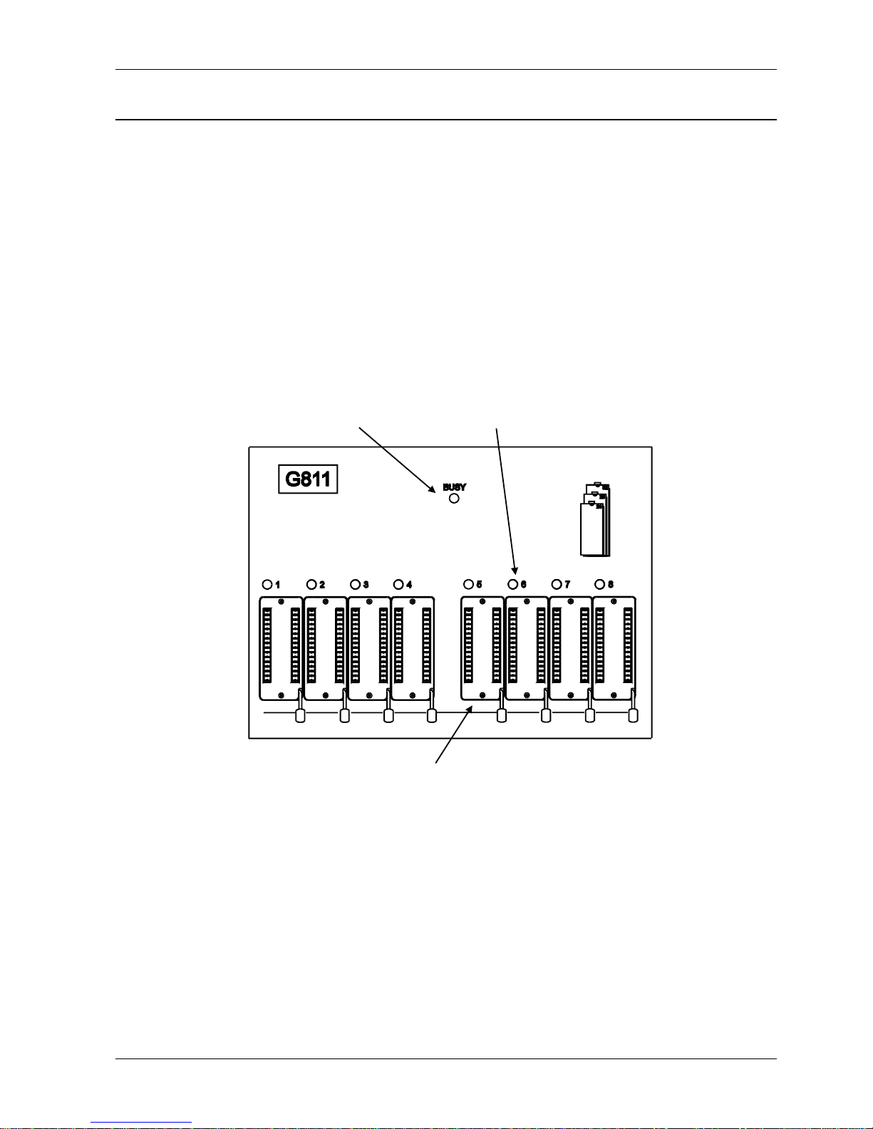
1.5 Modules
One module can be fitted at a time. Modules can either program 4 or 8 parts at a time. The
8 socket modules only support gang mode, but 4 socket modules can support different bit
modes see section 2.3 (below).
When a part is selected that the module supports, the Busy LED will go out.
! If the BUSY LED is red, parts must not be inserted into the sockets.
To remove a module move the lever behind the module (see figure 1, page 4) towards the
middle of the module and remove the module using the indents at the front and back of the
module. Move the lever back to the left hand side.
To insert a module, ensure the module removal lever behind the module is to the left. Push
module into place. Busy LED Socket LED’s
.
Sockets
figure 3
The module can be inserted or removed while the unit is powered up, but should not be
inserted or removed while the unit is performing a device function (e.g. load or program).
This is indicated by the busy LED being green.

P801 Operating Manual 7
2 Local Operation
All functions are menu driven. Use the ↑and ↓keys to select the required option, then
press ENTER.
The option which will be selected is always the 2nd row on the display. This is indicated by
the arrows formed in the display surround.
To abort from the menu:
!EXIT. (The pointing finger symbol denotes a dedicated function key press).
2.1 Device Selection
!DEV
Once DEV has been pressed the device code may be entered directly using 0-9, A-F. To
edit the code use the ←and → keys. When correct press ENTER.
Or
use the ↑and ↓keys to select the required manufacturer, then press ENTER. Now use the
←and → keys to select the required family or size of device, then the ↑ and ↓keys for the
exact device, finally press ENTER.
When selecting a new device, the bit mode may change, the device limits will be reset to
default values, and the security setting will be reset to unprogrammed.
2.2 Device Functions
Device functions will first perform a reverse part check to ensure that the devices are the
correct way round. If a part is faulty it may also fail this test. If this passes, a connect test is
performed, to ensure that devices are present in the correct sockets.
See the marking on the module for correct orientation of the package.
DIL devices should be inserted towards the front of the ZIF with pin 1 towards the rear
of the machine.
!
! !
! Before a device function is executed the user should ensure that all devices are
the same as the device selected. (See also Section 2.4.3 Electronic Identifier)
DIL devices should be inserted into the socket with the ZIF handle up; the handle should
then be lowered. The handle should be raised before the part is removed.
!
! !
! If the BUSY LED is red, parts must not be inserted into the sockets on that
module (see section 1.5 Modules)

P801 Operating Manual 8
The BUSY LED will go green, during a device function.
!
! !
! Devices or modules should not be removed, or added during a device function,
while the BUSY LED is green.
At the end of the function the display will indicate if the function passed or failed. All devices
that pass will have a green LED lit adjacent to them; all devices that fail will have a red LED
lit adjacent to them.
If a device fails, the red LED will light as soon as the failure is detected but the programmer
will continue until the function is completed, or all devices fail.
If a device is incorrectly placed in a socket, the P801 may not be able to detect its presence,
so the adjacent LED will be turned off. The isolation will ensure that the other parts program
correctly, but it is possible that the part in the adjacent socket may not be programmed, this
would be indicated by a red LED in that position.
If a device function is selected, when no, or an incorrect module is connected, then the
function will abort with the message
'No or incorrect Module Requires: xxxx'
where xxxx is the name of the required module.
2.2.1 Loading the P801's RAM from Master Devices
Master devices should be placed in the sockets starting at socket 1 on the left hand side
module.
The number of parts required depends on the mode selected (see Section 2.3).
!LOAD
On pressing LOAD the data in the device will be copied into the P801's internal RAM.
Remove master devices from the sockets after loading.
2.2.2 Verify
This function compares the contents of RAM with the data in the device(s). Some devices
will be verified twice at different VCC values as directed by the manufacturer's specification.
This will also happen if marginal verify is selected (see Section 2.4.2).
Ensure devices to be checked are inserted
!VERIFY

P801 Operating Manual 9
2.2.3 Empty
This function will check that the devices are unprogrammed. If an electrically erasable part
is selected, the part can be erased during programming, so new devices may not be
shipped in their empty state.
Ensure devices to be checked are inserted
!EMPTY
2.2.4 Program
This function initiates the automatic programming sequence. The device is first checked
with the pre-program check & erased if necessary (see Section 2.4.1), programmed with the
data in the RAM to the manufacturer's specification, verified, then the security fuses may be
blown if applicable (see Section 2.4.4).
Ensure devices to be programmed are inserted
!PROGRAM or PROG
Note there is no difference between pressing the PROG or PROGRAM buttons either can
be used.
2.3 Bit modes
The 8 Socket modules (named G8xx), are gang only (i.e. all sockets programmed with the
same data). 4 socket modules support different bit modes, as listed below:
For 8 bit parts
Mode Description
8 bit gang 4 sets of 1 part
8 bit 2of2 2 sets of 2 parts
8 bit 1of4 1 set of 4 parts
16 bit gang 2 sets of 2 parts with 16 bit wide data
16 bit 1of4 1 set of 4 parts with 16 bit wide data
32 bit gang 1 set of 4 parts with 32 bit wide data
For 16 bits parts
Mode Description
16 bit gang 4 sets of 1 part
16 bit 2of2 2 sets of 2 parts
16 bit 1of4 1 set of 4 parts
32 bit gang 2 sets of 2 parts with 32 bit wide data
The bit mode is used in all device functions (e.g. Load or Program), and can also be used
when calculating the checksum and CRC.

P801 Operating Manual 10
!MODE then select required mode.
Note that if the device is 16 bits wide then two bytes of RAM are required to store each
device word. This can be done either high byte first/low byte last (the default), or else low
byte first/high byte last. Having selected the bit mode as detailed below you will then be
asked to specify the byte order. To do this use the ←and →keys to make the selection,
then press ENTER when ready.
The mode may be changed on power up, or when a new device is selected, for example if
the mode requires more RAM than the P801 has. Not all modes are available for all parts.
2.3.1 8-bit Gang
In 8 bit GANG mode all sockets map to the same RAM image. Device data is stored in one
contiguous region of RAM. Loading is done from socket 1.
2.3.2 8-bit 2of2 (2 sets of 2 parts)
In 2of2 set mode data in the RAM is stored in two blocks, one block for sockets 1 and 3,
followed by one block for sockets 2 and 4. The block size is the size of the device selected.
- Sockets 1 and 3 will program/verify with data starting at RAM START.
- Sockets 2 and4 will program/verify with data starting at (RAM START + device size).
Loading will over write any existing data in the RAM for all sockets. Devices are required in
sockets 1 and 2.
2.3.3 8-bit 1of4 (1 set of 4 parts)
In 1of4 set mode data in the RAM is stored in four blocks, one block for each socket. The
block size is the size of the device selected.
- Socket 1 will program/verify with data starting at RAM START.
- Socket 2 will program/verify with data starting at (RAM START + device size).
- Socket 3 will program/verify with data starting at (RAM START + (device size x 2)).
- Socket 4 will program/verify with data starting at (RAM START + (device size x 3)).
Loading will over write any existing data in the RAM for all sockets. 3 or 4 devices may be
present, as long as there are devices in sockets 1, 2 and 3.
2.3.4 16-bit Gang
In 16-bit GANG mode groups of 16 bit data may be programmed.
For an 8-bit wide device the mapping will be as follows:
Socket 1 2 3 4
ImageABAB
The data for image A will be stored at even locations in RAM, while the data for image B will
be stored at odd locations in RAM. Loading is done sockets 1 and 2 only.

P801 Operating Manual 11
In the case of 16-bit wide devices all 8 sockets will program with the same data. Two bytes
of RAM are required for each device word, and the order in which these are stored is (by
default) high byte first, low byte last. This default may be modified by the user (see section
2.3 above). Loading is done from socket 1.
2.3.5 16-bit 2of2 (2 sets of 2 parts)
This mode is available for 16 bit wide parts only.
In 2of2 set mode data in the RAM is stored in two blocks, one block for sockets 1 and 3,
followed by one block for sockets 2 and 4. The block size is the size of the device selected.
- Sockets 1 and 3 will program/verify with data starting at RAM START.
- Sockets 2 and4 will program/verify with data starting at (RAM START + device size).
Loading will over write any existing data in the RAM for all sockets. Devices are required in
sockets 1 and 2.
2.3.6 16-bit 1of4 (1 set of 4 parts)
For 8-bit wide devices data in the RAM is stored in two blocks, one block for the socket pair
1 and 2, with the second block for the socket pair 3 and 4. The block size is twice the size of
the device selected.
- Socket 1 will program/verify with data starting at RAM START.
- Socket 2 will program/verify with data starting at (RAM START + 1).
- Socket 3 will program/verify with data starting at (RAM START + (device size x 2)).
- Socket 4 will program/verify with data starting at (RAM START + (device size x 2) +1).
Loading requires 4 devices, one in all 4 sockets.
For 16 bit parts data in the RAM is stored in four blocks, one block for each socket. The
block size is the size of the device selected.
- Socket 1 will program/verify with data starting at RAM START.
- Socket 2 will program/verify with data starting at (RAM START + device size).
- Socket 3 will program/verify with data starting at (RAM START + (device size x 2)).
- Socket 4 will program/verify with data starting at (RAM START + (device size x 3)).
Loading will over write any existing data in the RAM for all sockets. 3 or 4 devices may be
present, as long as there are devices in sockets 1, 2 and 3.
2.3.7 32-bit Gang
In 32 BIT GANG mode, groups of 32 bit data may be programmed.
For an 8-bit wide device the mapping will be as follows:
Socket 1 2 3 4
ImageABCD
The data for image A will be stored at addresses ending 0, 4, 8 and C (hex) the data for
image B will be stored at addresses ending 1, 5, 9 and D (hex), the data for image C will be

P801 Operating Manual 12
stored at addresses ending 2, 6, A and E (hex) and the data for image D will be stored at
addresses ending 3, 7, B and F (hex).
Loading will over write any existing data in the RAM for all sockets. 4 devices must be
present.
For a 16-bit wide device the mapping will be as follows:
Socket 1 2 3 4
ImageABAB
The data for image A will be stored at addresses ending 0-1, 4-5, 8-9, C-D (hex), the data
for image B will be stored at addresses ending 2-3, 6-7, A-B, E-F (hex). Note that two bytes
of RAM are required for each device word. The order in which these are stored is (by
default) high byte first, low byte last. This default may be modified by the user (see section
2.3 above).
Loading is done from the sockets 1 and 2 only.
2.4 Programming Sequence
This allows the user to define what functions are performed when a device operation is
required.
!Press SEQ
Sub-menus are selected using the ↑and ↓keys, then pressing ENTER.
2.4.1 Pre-program checks
!SEQ then select PRE-PROGRAM
Before a device is programmed, the device can be automatically checked with either an
empty check or an illegal bit check or neither.
The empty check checks that the device (within the specified device limits) is empty.
The Illegal bit check checks that the device has no bits which are programmed and required
to be empty by the RAM data.
Select using the ↑and ↓keys, then press ENTER.
On a electrically erasable device (e.g. EEPROM, Flash), the illegal bit check is used to
unlock the device, where applicable.
On parts that erase in blocks (e.g. Flash), the illegal bit check is used to check if erase is
necessary, and then erase the part.
!
! !
! on EEPROM and Flash devices, the illegal bit check should be enabled, unless
the parts are guaranteed empty, and unlocked.

P801 Operating Manual 13
2.4.2 Marginal verify testing
!SEQ then select MARGINAL TESTING
After programming, during illegal bit test, and when the VERIFY key is pressed the device is
verified with the RAM. This can either be done at the manufacturer's recommended VCC
voltages (Marginal verify disabled), or at +/- 10% of the nominal VCC voltage (Marginal
verify enabled).
Note: The lower marginal voltage is also used during empty testing and illegal bit testing.
Select the required option using ←and →, then press ENTER.
2.4.3 Electronic Identifier
!SEQ then select ELECTRONIC ID
An Electronic Identifier exists in some EPROM and Flash devices. It can be used to check
or select a device before load/verify/empty check or program.
Three options are given: check, automatic, none.
NONE will not check the electronic identifier unless required by the
programming algorithm.
CHECK will check that the device(s) in the socket(s) are the same
as that selected. If not, the error message WRONG PART
will be displayed. NO SIG will be displayed if no signature
can be read from the device.
AUTOMATIC will read the identifier and try to select the correct device
code to match. It can only select devices of the same family
as that already selected.
If different family devices are inserted then the error
message MISMATCHED PARTS will be displayed.
Select the required option using the ↑and ↓keys, then press ENTER.
2.4.4 Security fuses
!SEQ then select SECURITY
Some devices have one or more security fuses, which can either secure the part, or disable
writing to it. The user can select to program them or leave them intact using the ←and →
keys followed by ENTER. With devices that have more than one security fuse they can be
selected using the ↑and ↓keys to display the other fuses, ENTER is then pressed once to
enter all the fuses.
On some EEPROMs and Flash the security feature can be used to make the device, or
blocks of the device write protected.

P801 Operating Manual 14
To find out more details of what each fuse does, for a particular part, see the back of the
device support list.
The security setting is reset to not secure when the P801 is powered up, or a new device is
selected, except when selected via AUTOmatic electronic ID.
2.4.5 Display Checksums
!SEQ then select DISPLAY CHECKSUMS
After programming, verifying, and loading, the RAM checksums may be displayed.
Note: The checksums displayed are of the RAM not the device, and so should not be used
to check if a part verified, or programmed correctly.
Select the required option using ←and →, then press ENTER.
After a device function, the checksums for sockets 5, 6, 7, 8 can be displayed by pressing
→.
2.5 Device Limits
All device functions (e.g. Load or Program) have 3 associated parameters:
DEV START the device address from which the function should start;
DEV STOP the device address at which the function should stop;
RAM START the RAM address from which the function should start;
These are also used when calculating the checksum and CRC and can be altered by the
user.
!LIMITS
Enter the addresses (in Hexadecimal) using 0-9, A-F.
The cursor can be moved using the ↑and ↓keys.
When correct press ENTER.
If invalid addresses are chosen (e.g. DEV START higher than DEV STOP) the ENTER key
will not let the user out of the function. If the EXIT key is pressed the limits will not be
changed.
This function can be disabled: see section 2.9.3 for details.
!
! !
! The default limits for a device will be used when a new device, or new mode is
selected.

P801 Operating Manual 15
2.6 RAM Functions
2.6.1 Listing and changing the RAM
!EDIT
The editor displays 4 addresses, one on each line. Each is in the following format:
aaaaaaaa hh ddd c
where:
aaaaaaaa is the RAM address in hex;
hh is the hex value stored at that location;
ddd is the decimal value stored at the same location;
c is the ASCII for that byte if printable
(if not, a SQUARE character is displayed).
The address can be changed using 0-9, A-F and by moving the cursor using ←and →. To
edit the data move the cursor right to the hex or decimal data fields, then overwrite the data.
To edit the next or previous byte use ↑or ↓.
When complete press ENTER then EXIT.
Data can be listed by changing the address as above and then pressing ENTER, or by
using the ↑and ↓to view the previous or next location. Press EXIT when finished.
This function can be disabled: see section 2.9.3 for details.
2.6.2 RAM data manipulation
These functions can be disabled: see section 2.9.3 for details.
The following functions can be performed on the P801's internal RAM:
FILL RAM
BLOCK MOVE
INSERT BYTES
DELETE BYTES
COMPLEMENT RAM
STRING SEARCH
!DATA
Select the function required using the ↑and ↓keys, then press ENTER.
2.6.3 Fill the RAM
This function allows you to fill the contents of RAM between selected limits with a selected
bit pattern.
!DATA then select FILL RAM

P801 Operating Manual 16
On selecting `FILL RAM' the following options are available:
Fill with Zeros (fill the RAM with 00 hex)
Fill with Ones (fill the RAM with FF hex)
Fill with Empty (fill the RAM with the empty state of the selected device)
Fill with Pattern (fill the RAM with a user defined pattern)
Select the option required using the ↑and ↓keys, then press ENTER.
If `Fill with Pattern' is selected the desired pattern should be entered in hex using 0-9, A-F.
The ←and →keys may be used to move the cursor to edit the pattern. The ASCII value of
the hex numbers is displayed underneath (if a printable value is entered).
When correct press ENTER.
!
! !
! Note that patterns are only considered legal if they are 1, 2 or 4 hex characters
long.
All the options will then ask for the address range over which the fill is to take place. The
options are:
ARBITRARY LIMITS
ENTIRE MEMORY
DEVICE LIMITS
Select the option required using the ↑and ↓keys, then press ENTER.
The three functions available are as follows:
ENTIRE MEMORY: This function fills the entire RAM with the specified pattern.
DEVICE LIMITS: This will only fill the RAM used for the selected part, taking
account of the selected device limits (see Section 2.6) and
mode (see Section 2.3 ).
Note that if the device address limits are set to only partially
cover the device then this function may actually fill non-
contiguous regions of RAM.
ARBITRARY LIMITS: This function will enable the user to fill RAM between
entirely arbitrary RAM limits. On selecting this option the
address limits should be entered in hex using 0-9, A-F and
↑, ↓, ← and →to move the cursor as required. When
correct press ENTER.
2.6.4 Move a block of data
!DATA then select BLOCK MOVE
This function allows data to be moved from one section of RAM to another.
There are no restrictions on the positioning of either the source block or the destination
block, other than that they must both fit within the physical available RAM. Source and
destination blocks may even overlap, should this be required.
On selecting `BLOCK MOVE' the RAM address of BLOCK START, BLOCK END, and
DESTINATION should be entered in hex using 0-9, A-F and ↑ ↓ ←and →to move the
cursor as required. When correct press ENTER.

P801 Operating Manual 17
2.6.5 Inserting bytes into RAM
!DATA then select INSERT BYTES
This function allows a pattern of bytes to be inserted into RAM at a specific location.
All data at or beyond (i.e. at higher addresses than) the insertion address will be moved
upward in memory by the number of bytes inserted. No data bytes are overwritten at the
insertion position - instead they move up to make room for the new data.
!
! !
! Note that as a result of this operation, the very last byte(s) in memory will be
lost.
First enter the address in RAM to insert the first byte, use 0-9, A-F, and ↑↓←and →to
move the cursor. When correct press ENTER.
Then the desired pattern should be entered in hex using 0-9, A-F. The ←and →keys may
be used to move the cursor to edit the pattern. The ASCII value of the hex numbers is
displayed underneath (if a printable value is entered). Up to 32 characters may be entered.
When correct press ENTER.
2.6.6 Deleting bytes from RAM
!DATA then select DELETE BYTES
This function allows a number of bytes to be deleted from RAM. All data at or beyond (i.e. at
higher addresses than) the deletion address will be moved down in memory by the number
of bytes specified.
Enter the address in RAM to delete the first byte and the number of bytes to be deleted (in
hex), use 0-9, A-F, and ↑↓←and →to move the cursor. When correct press ENTER.
2.6.7 Complementing the RAM
!DATA then select COMPLEMENT RAM
This function allows the data in RAM to be complemented between selected limits. This
means that every binary 1 in the RAM data is changed to a binary 0, and vice versa.
The address range over which the complement is to take place should then be selected.
The options are:
ARBITRARY LIMITS
ENTIRE MEMORY
DEVICE LIMITS
Select the option required using the ↑and ↓keys, the press ENTER.
The three functions available are as follows:
ENTIRE MEMORY: This function changes the entire RAM with the specified
pattern.

P801 Operating Manual 18
DEVICE LIMITS: This will only change the RAM used for the selected part,
taking account of the selected device limits (see Section
2.6) and mode (see Section 2.3).
Note that if the device address limits are set to only partially
cover the device then this function may actually fill non-
contiguous regions of RAM.
ARBITRARY LIMITS: This function will enable the user to change the RAM
between entirely arbitrary RAM limits. On selecting this
option the address limits should be entered in hex using 0-
9, A-F and ↑, ↓, ← and →to move the cursor as required.
When correct press ENTER.
2.6.8 Search the RAM for a data sequence (STRING SEARCH)
This function allows you to search for a string of bytes within specified RAM limits.
!DATA then select STRING SEARCH
The desired pattern should be entered in hex using 0-9, A-F. The ←and →keys may be
used to move the cursor to edit the pattern. The ASCII values of the hex numbers are
displayed underneath (if printable values are entered). Up to 32 characters may be entered.
When correct press ENTER.
The address range over which the search is to take place should then be selected. The
options are:
ARBITRARY LIMITS
ENTIRE MEMORY
DEVICE LIMITS
Select the option required using the ↑↓keys, then press ENTER.
The three functions available are as follows:
ENTIRE MEMORY: This function searches the entire RAM with the specified
pattern.
DEVICE LIMITS: This will only search the RAM used for the selected part,
taking account of the selected device limits (see Section
2.6) and mode (see Section 2.3).
Note that if the device address limits are set to only partially
cover the device then this function may actually fill non-
contiguous regions of RAM.
ARBITRARY LIMITS: This function will enable the user to search the RAM
between entirely arbitrary RAM limits. On selecting this
option the address limits should be entered in hex using 0-
9, A-F and ↑, ↓, ← and →to move the cursor as required.
When correct press ENTER.

P801 Operating Manual 19
2.6.9 Checksum of RAM data
!CSUM
This function will display the checksum of the whole RAM, the device(s)' limits of RAM, or
arbitrary limits defined by the user. Select the option required. If the device limits are
chosen, then a checksum of each sockets 1 to 4 will be displayed, calculated according to
the current bit mode. On a gang only module, only 1 checksum will be displayed, as all the
sockets are the same.
2.6.10 Cyclic Redundancy Check of RAM data
!CRC
Cyclic Redundancy Check provides a better representation of the RAM data than a
checksum as it takes account of the order of the data. The format is the same as
checksum.
2.7 Setting up the I/O
The I/O ports can be used to input and output data to or from the P801's internal RAM.
They can also be used to remotely control the unit.
2.7.1 Data Transfer Formats
This function enables the user to select the data format for input and output.
!I/O then select FORMAT.
A list of available I/O formats is displayed. These can be scrolled up and down using the ↑
and ↓ keys. Typically, you might have a choice between: STAG HEX, BINARY, STAG
BINARY, ASCII HEX SPACE, INTEL 16 BIT, INTEL 32 BIT, MOTOROLA S-REC. The actual
list of formats available will vary, depending on the device currently selected.
Select the required format using the ↑and ↓ keys, then press ENTER.
2.7.2 Selecting and setting up the port.
!I/O then select PORT
A list of parameters is displayed. These can be scrolled up and down using the ↑and ↓
keys. The option may be changed using the ←and →keys. When the whole menu is set-
up as required press ENTER.
SPEED: The speed of the RS232 port may be set to:
1200, 2400, 3600, 4800, 9600, 19K2, 38K4 or 115K2 baud.
STOP BITS: The number of stop bits transmitted after each byte on the RS232 port may
be set to 1 or 2.
Table of contents


