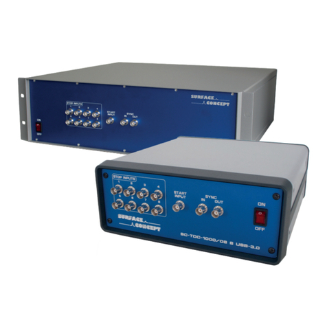
Surface Concept Octa Channel TDC User manual

Time-to-Digital Converter
Octa Channel TDC
(Release 442, 443, 451, 461)
Manual

2
Surface Concept GmbH
Am Sägewerk 23a
55124 Mainz
Germany
phone: +49 6131 62716 0
fax: +49 6131 62716 29
email: info@surface-concept.de
web: www.surface-concept.de
All rights reserved. No part of this manual may
be reproduced without the prior permission
of Surface Concept GmbH.
User Manual for the
Octa Channel TDC
Release 442, 443, 451, 461
Manual Version 2.4
Printed on 2021-08-06
Time-to-Digital-Converter Octa Channel TDC Manual | Surface Concept GmbH

3
Time-to-Digital Converter Octa Channel TDC Manual
1 Table of Contents.....................................................................................................................3
2 Introduction...............................................................................................................................5
2.1 General Information.........................................................................................................5
2.2 Safety Instructions ............................................................................................................5
3 Installation..................................................................................................................................7
3.1 Initial Inspection................................................................................................................7
3.2 Cabling..................................................................................................................................7
3.3 Software Installation, Requirements and Interface ........................................... 10
4 TDC Layout............................................................................................................................. . 11
4.1 Schematic Description of the Octa Channel TDC............................................... 11
4.2 Layout of the Octa Channel TDC .............................................................................. 13
4.2.1 TDC Stop Inputs ................................................................................................... 14
4.2.2 TDC Start Input..................................................................................................... 14
4.2.3 TDC Start Output ..................................................................................................15
4.2.4 Device Synchronization Signal Input/Output............................................15
4.2.5 Start Frequency Divider .....................................................................................16
4.2.6 Tag Signal Input ....................................................................................................16
4.2.7 Master Reset Input...............................................................................................17
4.2.8 State Signal Input .................................................................................................18
4.2.9 Shutter Signal Input.............................................................................................18
4.2.10 Gate Signal Output............................................................................................19
4.2.11 IP Address Setting and Hardware Reset ....................................................19
5 Technical Data.........................................................................................................................21
6 List of Figure ............................................................................................................................25
1 Table of Contents
Time-to-Digital-Converter Octa Channel TDC Manual | Surface Concept GmbH

4Time-to-Digital-Converter Octa Channel TDC Manual | Surface Concept GmbH
This side has been left blank on purpose.

5
Time-to-Digital Converter Octa Channel TDC Manual
2 Introduction
2.1 General Information
This manual is intended to provide an overview of the Octa Channel TDC in Release 442, 443, 451 and 461
as part of a delayline detector package. It is divided into 6 chapters. The chapter “Introduction” contains
a brief description of the device. The chapter “Installation” refers to installation and cabling. The other
chapters contain amongst others technical details and the description of the device layout.
2.2 Safety Instructions
The “caution symbol” marks warnings, which are given to prevent an accidental
damaging of the detector or the readout system. Do NOT ignore these warnings and
follow them strictly. Otherwise no guarantee is given for arose damages.
The following symbols appear throughout the manual:
Note
The “note symbol” marks text passages, which contain important information/hints
about the operation of the detector. Follow these information to ensure a proper
functioning of the detector.
The “high voltage symbol” marks warnings, given in conjunction with the description of
the operation/use of high voltage supplies and/or high voltage conducting parts.
Hazardous voltages are present, which can cause serious or fatal injuries. Therefore
only persons with the appropriate training are allowed to carry out the installation,
adjustment and repair work.
Please read this manual carefully before performing any electrical or electronic operations and strictly
follow the safety rules given within this manual.
Note
Please also respect the Surface Concept Device Safety Instructions Manual in addition
and all given safety rules within it.
Time-to-Digital-Converter Octa Channel TDC Manual | Surface Concept GmbH

6Time-to-Digital-Converter Octa Channel TDC Manual | Surface Concept GmbH
This side has been left blank on purpose.

7
Time-to-Digital Converter Octa Channel TDC Manual
3 Installation
3.1 Initial Inspection
Visual inspection of the system is required to ensure that no damage has occurred during shipping.
Should there be any signs of damage, please contact your provider immediately. Please check the delivery
according to the packing list (see Table 1) for completeness.
• Octa Channel TDC (R442, R443, R451, R461)
• 1x USB cable (R442)
• 1x Ethernet cable (R443, R451, R461)
• 1x power cable
Table 1: Packing list for the Octa Channel TDC (R442, R443, R451, R461)
3.2 Cabling
The general connection scheme of the delayline detector including its readout package is shown in the
corresponding delayline manual. A TDC specic connection scheme is given in Figure 1a - c.
Figure 1a: Specic connection scheme of the Octa Channel TDC R442 and R443 to a Surface Concept Delayline
Detector.
Time-to-Digital-Converter Octa Channel TDC Manual | Surface Concept GmbH

8
Figure 1c: Specic connection scheme of the Octa Channel TDC R461 to a Surface Concept Delayline Detector.
Figure 1b: Specic connection scheme of the Octa Channel TDC R451 to a Surface Concept Delayline Detector.
Time-to-Digital-Converter Octa Channel TDC Manual | Surface Concept GmbH

9
Time-to-Digital Converter Octa Channel TDC Manual
For all release versions
• First, use the„Ground” connector (M4 screw) to ground the device.
• Use the DLD readout cable/s to connect the “Lines Out” sockets on the front of the ACU with the“TDC
Input” sockets at the rear panel of the Octa Channel TDC.
• To perform time measurements with respect to an external clock, provide start pulses to the start input
of the TDC. Use the BNC socket named“START IN”to apply LVTTL (low voltageTTL) signals (see Chapter
4.2 for detailed information).
• Connect the power cable to the main connector.
• Install the TDC device driver or software package prior to switching on the TDC.
For release versions R442
• Use the USB cable to connect the Octa Channel TDC to the PC.
• Use BNC cables to connect your additional signals to the additional inputs of the TDC (e.g. TAG IN).
• Please note that all additional inputs are internally 50Ohm terminated and are laid out for 50Ohm
terminated LVTTL signal levels.
For release versions R443, R451, R461
• Use the Ethernet cable to connect the Octa Channel TDC to the PC.
• Use BNC cables to connect your additional signals to the additional inputs of the TDC (e.g. TAG IN).
• Please note that all additional inputs are internally 50Ohm terminated and are laid out for 50Ohm
terminated LVTTL signal levels.
Finish the complete cabling before the TDC is turned on and the GUI software is started.
Also, close the software and turn o the TDC before performing any changes to the
cabling.
This applies especially to the connection and disconnection of the start input of the TDC.
The start input of the TDC cannot handle pulses which are arriving in a time interval of
smaller than 120ns, as they are produced by e.g. connecting to and disconnecting from
the start input respectively.
If two subsequent pulses are applied to the start input of the TDC, the device will still
deliver results, but these results will contain wrong timing information.
Time-to-Digital-Converter Octa Channel TDC Manual | Surface Concept GmbH

10
3.3 Software Installation, Requirements and Interface
All operation functions of the TDCs for data readout of the detector package are encapsulated in a dynamic
linked library (scTDC1.dll). Data processing and presentation on the PC is realized by an end-user software
(e.g. GUI). See the corresponding software manual for detailed information on the software package and
the DLL interface.
The delivery package of the delayline detector includes a storage medium with hardware drivers and the
GUI software. Connect the storage medium to your PC and install the software package as described in the
Software Installation Manual.
Read-out of the TDC is done with a standard PC via USB (R442) or Ethernet (R443, R451, R461) connection.
For the PC the following minimum system requirements are highly recommended:
• Processor: Quad Core
• RAM: 4GB
• Windows 7 or higher
• USB connection (no front panel connector) (R442)
• Ethernet connection (R443, R451, R461)
Note
For release version R442
Depending on the specic PC system used for the TDC readout (mainly depending on
the specic USB3.0 chip used on the PC motherboard), the use of USB3.0 can lead to
instabilities in the data communication. For those cases we recommend the use of USB2.0.
The use of USB2.0 is always possible, but there might be limitations in the maximum
count rates for certain detector types and/or detector operation modes.
Time-to-Digital-Converter Octa Channel TDC Manual | Surface Concept GmbH

11
Time-to-Digital Converter Octa Channel TDC Manual
4 TDC Layout
4.1 Schematic Description of the Octa Channel TDC
The Octa Channel TDC series combines the excellent performance of the GPX TDC chip with a high speed
USB (R442) or an Ethernet interface (R443, R451, R461).
A eld programmable gate array (FPGA) enables a comfortable setup and a variable data stream handling
from the TDC via USB and Ethernet.
The main delayline detector functionality is permanently programmed. A complex FIFO design makes
data losses almost impossible. The user DLL controls the data handling and streaming for the user.
The following brief description about the internal structure of the measurement unit is only informative:
Figure 2a: TDC block diagram (R442).
Time-to-Digital-Converter Octa Channel TDC Manual | Surface Concept GmbH

12
Figure 2b: TDC block diagram (R443, R451, R461).
The stop pulses are distributed via an input unit to the dierent stop inputs of theTDC, in a specic manner
depending on the specic device layout. The arrival times of the pulses are measured by the TDC with
respect to either an internal reference start signal, provided by the FPGA, or an external start signal. An
internal electronics provides the TDC start signal to an additional BNC socket (“START OUT”) for further
extended measurement use. The measurement dwell times for data from the TDC are settled within the
FPGA by a quartz stabilized time gate in an interval from 1ms to 1193h. The synchronization pulse for the
external acquisition start (“SYNC IN”) is transferred directly into the FPGA that controls the acquisition
process. The FPGA also sends out a synchronization pulse for marking the end of an acquisition (“SYNC
OUT”). Additional counter inputs (e.g.“TAG”) and other inputs for advanced measurements are available.
The TDC data streaming is performed with a specic pre-conditioning of the DLD data, which includes
channel pairing, pair result arithmetic and many more. Communication to and from the PC is achieved
via a USB or Ethernet interface. Data streaming via the interface is provided without losses using a large
memory buer within the device.
Time-to-Digital-Converter Octa Channel TDC Manual | Surface Concept GmbH

13
Time-to-Digital Converter Octa Channel TDC Manual
4.2 Layout of the Octa Channel TDC
1. Device Ground Connection (R442, R443, R451, R461)
2. TDC Service Port, Ethernet socket for setting of static device IP address and hardware reset (R442, R443,
R451, R461)
3. Power Socket (R442, R443, R451, R461)
4. BNC Socket for SHUTTER Input (R442, R443, R451, R461)
5. BNC Socket for TAG Input (R442, R443, R451, R461)
6. BNC Socket for MASTER RESET Input (R442, R443, R451, R461)
7. BNC Sockets for Device Synchronization Signal IN and OUT (R442, R443, R451, R461)
8. BNC Sockets for external START Input and general START Output (R442, R443, R451, R461)
9. BNC Socket for STATE Input (R442, R443, R451, R461)
10. 1x HDMI Socket (R451), 2x HDMI Sockets (R461), 4x HDMI Socket (R442, R443) named TDC 1 - TDC 4 for
DLD Readout Cable from ACU with M3 Thread for Strain Relief
11. BNC Socket for GATE Output (R442, R443, R451, R461)
12. USB Connection Socket (R442) and Ethernet connection Socket (R443, R451, R461)
Figure 3: Layout of the Octa Channel TDC.
1
2
3
4567
12
8
910 11
13
Time-to-Digital-Converter Octa Channel TDC Manual | Surface Concept GmbH

14
4.2.1 TDC Stop Inputs
The Octa Channel TDC provides 1x (R442, R443), 2x (R451) and 4x (R461) HDMI sockets (“TDC 1” - “TDC 4”)
for 16 (R442, R443), 8 (R451) and 4 (R461) signal inputs from the ACU. The TDC inputs are laid out for PECL
signal levels.
13. Power Switch to turn the TDC ON/OFF. Lighted, when set to ON (R442, R443, R451, R461)
Take care that measurements are performed either with the internal start signal (Ext_
Gpx_Start = 0 respectively = NO) and no signal applied to theTTL Start Input (BNC socket)
or with an external start signal (Ext_Gpx_Start = 1 respectively = YES) applied to the TTL
Start Input. In all other cases the TDC is not working correctly.
Note
4.2.2 TDC Start Input
An external start signal must be provided to the TDC for real time resolved measurements. The external
start signal must be applied as a LVTTL (minimum amplitude of at least +2.1V on 50Ohms) signal to the
“Start In” (BNC socket). The start signal must always be in 50Ohm technique as the “Start In” is terminated
with 50Ohms internally within theTDC. In addition the software must be set to accept external start signals,
by changing the corresponding entry in the tdc_gpx3.ini le.
The corresponding entry in the tdc_gpx3.ini le is:
Ext_Gpx_Start = X
X is either NO or YES. The default setting is NO.
“Ext_Gpx_Start” = YES must be set for the TDC to accept the external start signal.
In addition the following entries in the tdc_gpx3.ini must be set as follows:
StartCounter = YES
StartPeriod = 0x800000
Measurements are performed in respect to an internal start signal of the TDC when “Ext_Gpx_Start” =
NO. This internal start signal has no time correlation to any external clock and therefore also not to the
incoming stops. The internal start signal can be used for pure 2D(x, y) measurements. Any external start
signal must be disconnected from the start input of the TDC, when working with the internal start signal.
The rise time of the external start signal is of great importance, the faster the rise time, the better the time
resolution. The maximum frequency of the start pulse must not exceed 9MHz.
Note
Do not forget to save the ini le after any changes you make and restart the software. For
further information check the software manual.
Time-to-Digital-Converter Octa Channel TDC Manual | Surface Concept GmbH

15
Time-to-Digital Converter Octa Channel TDC Manual
The start input of the TDC cannot handle pulses which are arriving in a time interval
of smaller than 120ns (e.g. as produced by connecting/ disconnecting the start signal
during TDC operation). If two such subsequent pulses are applied to the start input of
the TDC, the device will still deliver results, but these results might contain wrong timing
information.
The maximum frequency for the start signal of 9MHz. Larger start pulse frequencies must
be divided down with an appropriate frequency divider (e.g. divider with factor of 16 for
80MHz start pulse frequency).
Note
The temporal resolution is inuenced mainly by the quality of the start signal because
the TDC measures the time in a leading edge determination. Therefore, if the start signal
is varying in time, one needs to process it by means of a constant-fraction-discriminator
or similar external electronics components.
4.2.4 Device Synchronization Signal Input/Output
The data acquisition can be synchronized to an external signal for various measurement applications linked
to external devices. This device synchronization signal has to be applied as LVTTL signal to the “SYNC IN”
(BNC socket) of the TDC. This functionality is switched on/o within the tdc_gpx3.ini le.
The corresponding entry in the tdc_gpx3.ini le is:
Ext_trigger = X
X is either NO or YES. The default setting is NO.
The TDC ignores any external synchronization signals if“Ext_trigger” = NO. In case that “Ext_trigger” = YES
and the “Sync In” signal is not provided, the device will not come to operation at all.
The TDC provides always a LVTTL signal on the “SYNC OUT” BNC socket after the end of each acquisition,
independent on the setting of“Ext_trigger”.
TheTDC holds an internal electronics, which provide theTDC start signal for further extended measurement
use. The “START OUT” (BNC socket) provides either the external start if applied or the internal start,
generated by the FPGA.
4.2.3 TDC Start Output
Note
Do not forget to save the ini le after any changes you make and restart the software. For
further information check the software manual.
Time-to-Digital-Converter Octa Channel TDC Manual | Surface Concept GmbH

16
4.2.6 Tag Signal Input
The tag input is an additional counter input for signal counting. The counter number is included into the
general data stream of the TDC. The tag signal has to be applied as a LVTTL (low voltage TTL) signal on
50Ohms to the“TAG IN“ (BNC socket) of the TDC.
In addition changes in the tdc_gpx3.ini le must be made for the tag signal to be registered by the TDC.
The corresponding entry in the tdc_gpx3.ini le is:
TimeTag = X
X is an integer value and must be one of the following values: 0, 1, 2, 3, 4, 5 or 6.
The default setting is 0.
Each value represents a certain functionality, which is described below:
4.2.5 Start Frequency Divider
The maximum start frequency for the Octa Channel TDC is restricted to 9MHz. To cope with larger start
frequencies the Octa Channel TDC is equipped with an internal start frequency divider for external start
frequencies of up to 150MHz (this mode only works when using the external start input). Herewith the
frequency divider can operate with dierent dividing factors, which can be set within the software, to
always guarantee a start frequency of below 9MHz.
The frequency divider is switched on/o within the tdc_gpx3.ini le, in which also the dividing factors are
set.
The corresponding entry in the tdc_gpx3.ini le is:
Start_Divider = X
X is an integer value and must be one of the following values: 0, 2, 4, 8, 16 or 32. The value 1 is not allowed.
The default setting is 0
X = 0 switches o the start divider and leads to normal operation without dividing the start frequency.
The time histogram will appear X times in series, when using a dividing factor of X. This is due to the fact
that only each 1st start pulse out of a sequence of X start pulses will be accepted as start signal, while all
stop signals are detected. This leads to the multiple time histograms that appear sequentially in time. The
multiple histograms can be resorted to one single time histogram by a MODULO-operation during data
analysis.
Time-to-Digital-Converter Octa Channel TDC Manual | Surface Concept GmbH

17
Time-to-Digital Converter Octa Channel TDC Manual
4.2.7 Master Reset Input
The master reset input is treated as an additional sign signal within the TDC and is counted up in a software
counter within the dll.
In addition the master reset input is connected to the reset pin of the TDC chip. Each time a signal is
applied to the master reset input the corresponding software counter is counting up and the input and
output FIFOs of the TDC chip are cleared (all old TDC data are erased).
A LVTTL (low voltage TTL) signal on 50Ohms has to be applied to the “MASTER RESET IN“ (BNC socket) of
the TDC.
TimeTag = 0
TimeTag = 1
TimeTag = 2
TimeTag = 3
TimeTag = 4
TimeTag = 5
TimeTag = 6
;tag counting is switched o and any signal to the “TAG IN“ is ignored, nBytes can be
set to 4 or 8 (see below for further details on nBytes). Also any state input, master reset
input or ADC input signals are ignored.
;the tag is counting the internal 80MHz clock signal of the FPGA and is therefore
functioning as a timer. Any signal to the“TAG IN“ is ignored. This mode is not working in
combination with the state input.
;the tag is counting the external LVTTL signal applied to the “TAG IN“. The counter is
reset with the start of a new measurement. This mode is not working in combination
with the state input.
;tag counting is switched o and any signal to the“TAG IN“ is ignored. This value must be
set for using the ADC functionality in combination with the state input and the master
reset input.
;corresponds to the setting of TimeTag = 3.
;must be set for using the tag as timer (similar to TimeTag = 1) but in combination with
the state input. A pulse on“TAG IN“ resets the timer to 0.
;must be set for using the tag as counter (similar toTimeTag = 2) but in combination with
the state input.
The number of bits which are available for each detector event (x, y, t) is dened by an additional parameter
called “nBytes” in the tdc_gpx3.ini le.
The corresponding entry in the tdc_gpx3.ini le is:
nBytes = X
X is an integer value of either 4 or 8. The default setting is 8.
Time-to-Digital-Converter Octa Channel TDC Manual | Surface Concept GmbH

18
4.2.8 State Signal Input
The state signal has to be applied as a LVTTL (low voltage TTL) signal on 50Ohms to the “STATE IN“ (BNC
socket) of the TDC.
In addition, the value of the variable named “TimeTag”in the tdc_gpx3.ini le (depending on the software
version which is used) must be adapted for the state signal to be registered by the TDC.
The state signal input assumes values 0 or 1, depending on the given electronic level of the LVTTL signal
(low or high).
For the state input to be functioning the following variables in the tdc_gpx3.ini must be used:
TimeTag = 3
TimeTag = 4
TimeTag = 5
TimeTag = 6
;must be set for using the state input in combination with the ADC functionality and
the master reset input. The tag counting is switched o and any signal to the “TAG IN“
is ignored.
;corresponds to the setting of TimeTag = 3
;must be set for using the state input. Hereby the state input functions in combination
with the tag signal functioning as a timer, counting the internal 80MHz clock signal of
the FPGA. A signal on“TAG IN“ resets the timer to 0.
;must be set for using the state input. Hereby the state input functions in combination
with the tag signal functioning as a counter, counting the external LVTTL signal applied
to the“TAG IN“.
4.2.9 Shutter Signal Input
The shutter signal allows to prevent stop signals which belong to a specic start signal to be respected by
the TDC. Each time a new start signal is applied (independent if it is an external start signal or an internal
one), the TDC checks if the shutter signal is applied. In case it is applied (high level on the shutter input),
the TDC ignores all incoming stop signals which belong to that specic start signal, meaning all incoming
stop signals are ignored and not fed into the data stream until the next start signal arrives, at which point
the shutter signal is checked again. Independent on if the shutter signal is applied or not, each start signal
is counted by the start counter.
The shutter signal has to be applied as a LVTTL (low voltage TTL) signal on 50Ohms to the “SHUTTER IN“
(BNC socket) of the TDC.
Time-to-Digital-Converter Octa Channel TDC Manual | Surface Concept GmbH

19
Time-to-Digital Converter Octa Channel TDC Manual
The TDC can provide an additional signal which is in correlation to the internal start signal of the TDC. This
signal is not provided with each internal start, but only once at the beginning of each measurement. It is
provided as a low voltage TTL signal to the “GATE OUT” (BNC socket) of the TDC.
The gate out signal can be used e.g. to extend the measurement range of the TDC from the standard
40µs to a virtual unlimited measurement range. For this it is necessary that the TDC triggers the time
resolving application/ source (e.g. laser system) of the customer instead of using a reference signal from
the customer’s application/ source as external start signal for the TDC. This is signicantly dierent to the
normal time resolved operation mode. The length of the extended measurement range is dened one
by one by the acquisition time of the measurement (e.g. an acquisition time of 10ms is used to dene a
measurement range of 10ms).
In addition changes in the tdc_gpx3.ini le must be made for the gate out signal to be provided by the
TDC.
The corresponding entry in the tdc_gpx3.ini le is:
Measurement_to_Start_Sync = X
X is either NO or YES. The default setting is NO.
“Measruement_to_Start_Sync” = YES must be set for the TDC to provide the gate out signal.
In addition the following entries in the tdc_gpx3.ini must be set as follows:
StartCounter = NO
StartPeriod = 0
4.2.10 Gate Signal Output
The TDC comes with a second Ethernet connector to allow to set the static IP Address of the TDC as well as
to allow a remote hardware reset.
The TDC itself can only handle static IP addresses but no dynamically ones given via DHCP. It comes with
a predened factory IP address, which can be used to connect the TDC to a PC. In this case the TDC must
be connected directly to a free network connector of the PC (it is recommended to use a PC with a second
network connector available, so that the rst one can be used for connecting the PC to a general network).
The network port of the PC must be congured accordingly to the IP address of theTDC which is as follows:
static IPv4 address (predened factory address): 10.0.0.20
subnet mask: 255.255.255.0
4.2.11 IP Address Setting and Hardware Reset
Time-to-Digital-Converter Octa Channel TDC Manual | Surface Concept GmbH
See also the DLD Device Driver and Software Installation Manual for further details.
Note

20 Time-to-Digital-Converter Octa Channel TDC Manual | Surface Concept GmbH
The IP address can be changed to adapted to the conguration of a local existing network.
This would allow to connect the TDC to any Ethernet connector of the network. None the
less, it is strongly recommended to connect the TDC directly to the PC anyway, because
otherwise the maximum data transfer (and with this connected any maximum transferred
count rate) is depending on the current load of the network.
Note
The IP address of the TDC is also given in the tdc_gpx3.ini le. Therefore the corresponding entry in the in
le must be adapted for any change of the IP address.
The corresponding entry in the tdc_gpx3.ini le is:
sn = “XXX.XXX.XXX.XXX/Y”
XXX.XXX.XXX.XXX is the IP address of the device, while y is a device index in case that more than one TDCs
are connected at a time to the PC.
The default setting is 10.0.0.20/1
To change the IP address one must connect the TDC to a network using the TDC service port (see Chapter
4.2). This connects to an internal service module, which handles its own, separate IP address, which can be
received from any local network via DHCP.
Commands to change the IP address must be passed as command lines via this service module. This can
be done by using any SSH and telnet client software. To connect to the TDC via the service port one must
provide the host name of the TDC as well a port number. The corresponding entries are:
host name: scXXXXXXXXXX
port: 2553
XXXXXXXXXX are the last 10 digits of the serial number, which can be found on a sticker on the back side
of the TDC (e.g. 4517719001).
Instead of using the host name, one can also enter the IP address directly. But here it is refereed to the IP
address of the internal service module, which is often unknown, because it is received via DHCP. None the
less, this might be necessary to do, in cases where no DNS service is available in the network. The DNS
service is necessary to link the host name with the IP address of the service module.
i XXX.XXX.XXX.XXX
fr
w
XXX.XXX.XXX.XXX is the new IP address of the device, while i is the device index.
The default setting for i is 0.
Resets the TDC itself.
Resets the service module.
The following commands for the service module are available:
Table of contents
Other Surface Concept Media Converter manuals
Popular Media Converter manuals by other brands

PRAGMATIC COMMUNICATIONS SYSTEMS
PRAGMATIC COMMUNICATIONS SYSTEMS DMS 4.4 instructions
Magewell
Magewell XI006AUSB user guide

Ross
Ross MB-652-DUO Installation and Cabling
Beresford
Beresford ASYNCH-1 installation manual

Optelecom-nkf
Optelecom-nkf XSNet 1600 MC user manual
Korenix
Korenix JetCon 2302 user manual
Lika
Lika AMM5A / BG1 Series user guide
Pro-Ject Audio Systems
Pro-Ject Audio Systems BOX DESIGN Stream Box DS2 T instruction manual
ACTiSYS
ACTiSYS IR9201 user manual
JB Systems
JB Systems USB AUDIO CONVERTER Operation manual
Extron electronics
Extron electronics Multi Video Processor MVP 104 Specifications

Anttron
Anttron TMX160HD user manual
