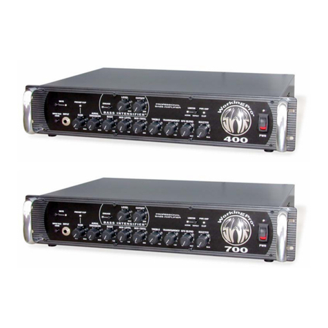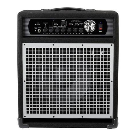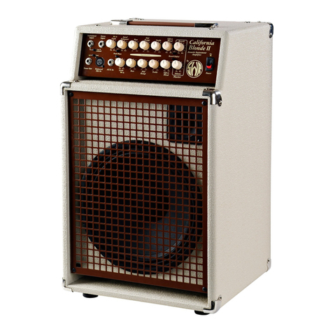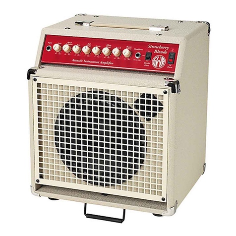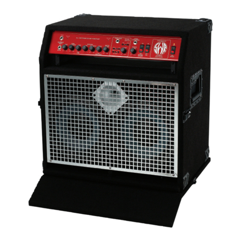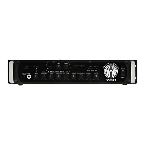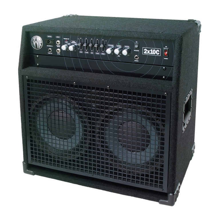
SPELLBINDER BLUE™
(This is the model name for warranty claims)
5
PCB EXCHANGE POLICY
Parts marked with a single asterisk (*) in the Part
Lists are not field replaceable. If a failure due to
one of these components is detected, please con-
tact the FMIC Customer Service Department to
order the complete PCB Assembly.
CIRCUIT DESCRIPTION
This section provides concise information about new
or unusual circuitry designs incorporated into this
amplifier model. The purpose is to aid the service
technician by providing insight into the design areas
most likely to become obstacles in troubleshooting.
Information is focused for its effective use while
maintaining the security of Fender® proprietary in-
formation wherever possible.
Preamp PCB:
The following discussion follows the signal path
through the functional blocks of the amplifier. The
signal is introduced at J8-A (XLR) or J8-B (¼”). The
XLR input will see a 20kΩinput impedance while
the ¼” input will see a 4.7MΩinput impedance. U6A
provides a gain of 10 for the XLR input while the ¼”
input goes directly into the tube gain stage of V1-A.
The GAIN stage at U7A provides up to 1.1X gain,
followed by the PHASE reversal stage at U5A. This
allows the phase of the channel to be changed 180°
depending on the position of S3.
The EQ IN/OUT Switch (S6) selects either the pas-
sive Aural Enhancer circuit (the classic circuit found
in other SWR bass amplifiers) or the active attenua-
tion of U5B. The signal then goes to the second
tube stage at V1-B.
Following the tube buffer at U13A is the EQ circuitry
comprising U9A&B, U10A and U13B. This architec-
ture is similar to the SWR Baby Baby Blue amplifier,
and boosts or attenuates each frequency range by
+/-15dB. The frequency response of this stage is
flat when all of the level knobs are at their center-
detent position.
S6-D selects the post-EQ path from U13B or the
pre-EQ path from U13A. From here the signal goes
to the Effects Send buffer at U11A, the EFFECTS
BYPASS switch (S7), and also to the EFFECTS
BLEND pot (R91) which blends the Send and Re-
turn signal before U10B, which contains a -12dB/
octave high-pass filter.
U8B is the Compressor chip which works with U15A
to reduce the signal at this point when the COM-
PRESSION pot (R92) is turned clockwise. U8 pin
16 is a current driven pin. The circuitry for this cur-
rent is produced by U14A&B, U15B, and U16A&B.
The maximum amount of compression available is
approximately 20dB.
The MASTER Volume control (R93) is at U12A
which has a maximum gain of 3.5X. This stage and
the inverted signal at U12B serve as a gain buffer
for the power amp at P6.4 and P6.7.
The Preamp Clip Detect circuits operate simply by
monitoring several stages of the preamp. If any of
the sense points rise above the overload threshold
(approximately 12V), the Clip LED will be illumi-
nated.
The MUTE circuitry is engaged using S8. The
Speaker mute circuitry is on the Power Amp PCB
while the Balanced Line Output mute circuitry is on
the Rear Panel PCB.
Rear Panel PCB:
The Rear Panel PCB is a breakaway from the Pre-
amp PCB and is connected to the Preamp PCB
through a 12 circuit ribbon cable assembly (P7 on
the Preamp, P1 on the Rear Panel). The signals
