Tektronix, Inc. 326 User manual

INSTRUCTION MANUAL
Tektronix, Inc.
P.0. Box 500
Beaverton, Ore on 97005 Serial Number
070-1578-00 273

, ' - '.,/' ,>'~j z ? ';'‘'? > z r;- ‘. •* --* •" "
RANTY
nts are warranted again
kmanship f r ne year. An'
warranty sh uld be taken up
K J^|d Engineer r representative,
displacem ent parts sh uld be
OIMIX Field Office r representative
rey ur:
tu m ih i^ ^
ithii|t;-|i
i# pjr£pe'
fp^m aferiai
f Oreg n. Printed in the United States f
AmerMa: All rights reserved. C ntents f this publicati n
may n t be repr duced in any f rm with ut permissi n f
Tektr nix, Inc.
U.S.A. and f reign TEKTRONIX pr ducts c vered by U.S.
and f reign patents and/ r patents pending.
TEKTRONIX is a registered trademark f Tektr nix, Inc.
326 (SN 300500-up)
SECTION 1
SECTION 2
SECTION 3
SECTION 4
TABLE OF CONTENTS
SPECIFICATION Page SECTION 4 MAINTENANCE (c nt) Page
Intr ducti n 1-1 Recalibrati n 4-1
Electrical Characteristics 1-1 Tr ublesh ting Aids 4-1
Vertical Amplifier 1-1 Tr ublesh ting Equipment 4-1
Time Base 1-2 Replacement Parts 4-1
Calibrat r 1-2 Assembly and C mp nent Replace
External H riz ntal Input 1-2 ment 4-2
External Blanking 1-2 1 nstru ment R epackag i ng 4-6
CRT Display 1-3
P wer S urce 1-3
Internal Battery Supply 1-3
Envir nmental 1-3 SECTION 5 PERFORMANCE CHECK/ADJUSTMENT
Intr ducti n 5-1
OPERATING INSTRUCTIONS Test Equipment Required 5-1
Sh rt-F rm Perf rmance Check
P wer S urce Requirements 2-1 and Index 5-2
Functi n f External C ntr ls, Perf rmance Check Pr cedure 5-4
C nnect rs, and Indicat rs 2-3 Sh rt-F rm Adjustment Pr cedure
Instrument Familiarizati n 2-5 and Index 5-12
Adjustment Pr cedure 5-13
CIRCUIT DESCRIPTION
Intr ducti n 3-1 SECTION 6 ELECTRICAL PARTS LIST
Basic Bl ck Descripti n 3-2
MAINTENANCE SECTION 7 DIAGRAMS, CIRCUIT BOARDS
Intr ducti n 4-1
General 4-1
Cleaning 4-1 SECTION 8 MECHANICAL AND REPACKAGING
Semic nduct r Checks 4-1 PARTS ILLUSTRATIONS
ACCESSORIES

SONY/TEKTRONIX 326 Oscill sc pe.
326 (SN 300500-up)

326 SPECIFICATION
Secti n 1—326 (SIM 300500-up)
Intr ducti n
The SONY/TEKTRONIX 326 Oscilloscope is a solid-
state portable instrument that combines small size and li ht
wei ht with the ability to make precision waveform
measurements.
A dual-trace DC to 10 MHz vertical system provides
calibrated deflection factors from 0.01 Volt/Div to
10 Volts/Div (0.001 Volt/Div minimum with reduced
frequency response).
The tri er circuit provides stable tri erin over the full
vertical bandwidth. A 300 ns delay line in the vertical
system allows the operator to view the portion of the
waveform on which tri erin occurs.
The horizontal deflection system provides calibrated
sweep rates from 1 jUs/Div to 1 s/Div. A 10X ma nifier
extends the sweep rate to 0.1 jiis/Div.
The 326 can be operated from internal battery, an
external DC source, or from the AC line (with battery
char er attached).
The followin electrical characteristics apply over an
ambient temperature ran e of +20°C to +30° C (+68°F to
+86°F). Warmup time for the accuracies iven is approxi
mately 10 seconds.
CHARACTERISTICS
VERTICAL AMPLIFIER
Deflection Factor
Ran es: 10 mV/Div to lOV/Div in XI Gain and
1 mV/Div to 1 V/Div in X10 Gain. 10 steps in a 1-2-5
sequence. Accuracy within 3% over the calibrated ran e.
Variable: Variable between calibrated deflection factor
settin s. Extends the hi hest deflection factor to at least
25 V/Div.
Attenuator Compensation: +1%, —1%, or less, 0°C to
+55°C (+32°F to +131°F). +2%, -2%, or less, -15°C to
0°C (+5°Fto+32°F).
Frequency Response
Bandwidth (Variable Volts/Div at CAL, 4 division
reference) direct coupled: IX Gain, DC to at least
10 MHz (upper —3dB point) with the P6049A Probe.
Capacitively coupled, 4 division reference: from 10 Hz
or less (lower —3 dB point) at all deflection factors. 1 Hz
or less with the P6049A Probe.
Step Response (risetime), 4 division step input: 36 ns or
less in XI Gain and 72 ns or less with X10 Gain.
Aberrations: +2.5%, —2.5% with total of 4% or less in all
modes except ADD ALG. +3%, —3% with total of 6% or
less in ADD ALG Mode.
Input
Maximum Volta e: 500 volts direct coupled (DC + peak
AC) or capacitively coupled DC volta e.
Resistance: 1 M£2, within 2%, direct and 10 M£2, within
2%, with the P6049A Probe.
Capacitance: 47 pF within 4 pF direct and 13.5 pF or
less with the P6049A Probe.
Amplifier
Linear dynamic ran e in Added Mode: Equal to or
reater than 8 times the Volts/Div settin for 10%
distortion.
Common-Mode Rejection: At least 20:1 at 2 MHz for a
common-mode si nal of 80 mV peak-to-peak, Volts/Div
set at 10 mV and CH 2 set for maximum CMRR at
50 kHz and 10 mV.
DC Drift
With Time (short term): 0.2 div or less durin any
minute within the first hour after a 10 second
warmup (with temperature and line volta e constant).
1-1

Chopped Mode
Repetition Rate: 110 kHz within 20%.
Specificati n—326 (SN 300500-up)
TIME BASE
Sweep Time/Div
Calibrated Ran e: 1 s/Div to 1 /is/Div in 19 steps in a
1-2-5 sequence. 10X ma nifier extends the displayed
sweep time to 0.1 jus/Div.
Accuracy, XI Gain: within 3% over the center ei ht
raticule divisions from 1 jus/Div to 0.2 s/Div, increasin
to 4% from 0.5 s/Div to 1 s/Div.
X10 Gain: within 5% over any 2 division interval within
the center ei ht raticule divisions 1.0 jus/Div to
20 ms/Div. Increasin to 6% at 0.5 jus/Div, 0.1 jus/Div,
0.1 s/Div, and 50 ms/Div.
Variable: at least 2.5:1.
Tri er
Internal: DC to 10 MHz on si nals causin 1.0, or more,
division of vertical deflection and to approximately
1.0 MHz on si nals causin 0.3 division of vertical
deflection.
External: DC to 10 MHz on si nals of 500 mV or more,
decreasin to approximately 1.0 MHz on si nals of
150 mV.
Couplin : AC attenuates si nals below 30 Hz; LF REJ
attenuates si nals below 50 kHz.
External Level Ran e: Atten at X I, +0.8 V to -0.8 V;
Atten at X10,+8 V to —8 V.
Maximum Input Volta e: 300 V (DC + peak AC).
CALIBRATOR
Output
Volta e Accuracy (into a load of 1 M£2 or reater):
0.5 V, within 1% from +20°C to +30°C (+68°F to
+86°F), decreasin to within 2% from -15°C to +20°C
(+5°F to +68° F) and +30°C to +55°C (+86° F to
+ 131°F).
Duty Cycle: 40% to 60%.
Resistance: Approximately 10 k£2.
EXTERNAL HORIZONTAL INPUT
Deflection Factor
Horiz Ma X10, Ext Atten IX: 15 mV/Div to
25 mV/Div.
Horiz Ma off. Ext Atten IX: 150 mV/Div to
250 mV/Div.
Horiz Ma X10, Ext Atten 10X: 150 mV/Div to
250 mV/Div.
Horiz Ma off. Ext Atten 10X: 1.5 V/Div to 2.5 V/Div.
Bandwidth
DC to at least 200 kHz (upper —3 dB point).
Dynamic Ran e
At least 20 divisions (+2.5 volts to —2.5 volts) with EXT
TRIG OR HORIZ ATTEN switch set to X10, and EXT
HORIZ Variable control set to CAL.
Variable Ran e
At least 10:1.
EXTERNAL BLANKING
Sensitivity
DCCoupled: +5 volts to +20 volts.
Usable Frequency Ran e
To approximately 100 kHz.
Input Volta e
1-2
Maximum: 50 V (DC + peak AC).
Specification—326 (SIM 300500-up)
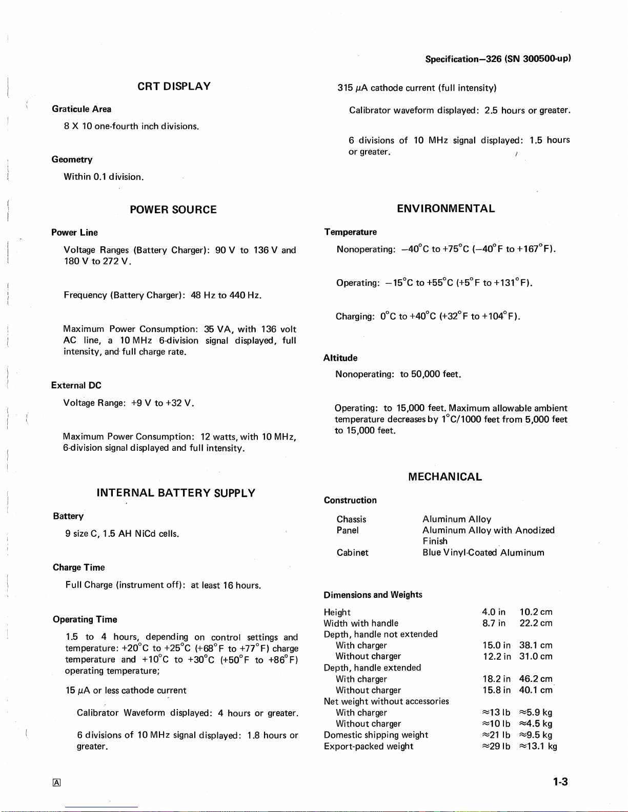
CRT DISPLAY 315 jjlA cathode current (full intensity)
Graticule Area Calibrator waveform displayed: 2.5 hours or reater.
8X10 one-fourth inch divisions. 6 divisions of 10 MHz si nal displayed: 1.5 hours
or reater. /
Geometry
Within 0.1 division.
POWER SOURCE
Power Line
Volta e Ran es (Battery Char er): 90 V to 136 V and
180 V to 272 V.
Frequency (Battery Char er): 48 Hz to 440 Hz.
Maximum Power Consumption: 35 VA, with 136 volt
AC line, a 10 MHz 6-division si nal displayed, full
intensity, and full char e rate.
External DC
Volta e Ran e: +9 V to +32 V.
Maximum Power Consumption: 12 watts, with 10 MHz,
6-division si nal displayed and full intensity.
ENVIRONMENTAL
Temperature
Nonoperatin : —40°C to +75°C (—40°F to +167°F).
Operatin : -15°Cto+55°C (+5°F to+131°F).
Char in : 0°C to +40°C (+32°F to +104°F).
Altitude
Nonoperatin : to 50,000 feet.
Operatin : to 15,000 feet. Maximum allowable ambient
temperature decreases by 1°C/1000 feet from 5,000 feet
to 15,000 feet.
INTERNAL BATTERY SUPPLY
Battery
9 size C, 1.5 AH NiCd cells.
Char e Time
MECHANICAL
Construction
Chassis Aluminum Alloy
Panel Aluminum Alloy with Anodized
Finish
Cabinet Blue Vinyl-Coated Aluminum
Full Char e (instrument off): at least 16 hours.
Operatin Time
1.5 to 4 hours, dependin on control settin s and
temperature: +20°C to +25°C (+68°F to +77°F) char e
temperature and +10°C to +30°C (+50°F to +86°F)
operatin temperature;
15 jiiA or less cathode current
Calibrator Waveform displayed: 4 hours or reater.
6 divisions of 10 MHz si nal displayed: 1.8 hours or
reater.
Dimensions and Wei hts
Hei ht 4.0 in 10.2 cm
Width with handle 8.7 in 22.2 cm
Depth, handle not extended
With char er 15.0 in 38.1 cm
Without char er 12.2 in 31.0 cm
Depth, handle extended
With char er 18.2 in 46.2 cm
Without char er 15.8 in 40.1 cm
Net wei ht without accessories
With char er «13lb ~5.9 k
Without char er «10lb ^4.5 k
Domestic shippin wei ht «21 lb ~9.5 k
Export-packed wei ht ~29lb ~13.1 k
1-3


Secti n 2-326 (SN 300500-up)
OPERATING INSTRUCTIONS
(
I
I
I
General
This section explains power source requirements,
describes the functions and uses of controls and connectors,
and ives first time and eneral operatin information.
POWER SOURCE REQUIREMENTS
WARNING I
The cells used in the battery pack are capable of
delivering a large a ount of energy in a short ti e.
Rings, watch bands and other etallic ite s that
ight short circuit the battery can rapidly beco e
hot enough to cause severe burns.
General
The 326 may be powered from either the internal
Battery Pack (nine NiCd cells connected in series) or on an
external DC volta e source ran in from +9 volts to +32
volts.
The internal battery pack is removable and may be
char ed (while in the instrument or externally) by the
battery char er.
Typical operatin time from a fully char ed battery pack
is approximately 4 to 5 hours. Actual operatin time varies
with sweep rate, the displayed si nal frequency and
amplitude, display bri htness, and the ambient temperature
durin cell char e.
Internal Battery Operati n
Slidin the power source switch to the BATT OR AC
ADPT position connects the internal battery to the 326
front-panel POWER switch. Internal battery powered
operation is not possible with the source switch in the EXT
DC POWER position.
Internal battery powered operation should be discon
tinued after the LOW BATT lamp starts flashin . The
battery should immediately be put on char e or the battery
pack should be replaced with a fully char ed pack.
If the internal battery-powered operation is continued
after the LOW BATT lamp starts flashin , the trace will
disappear in a short time and the LOW BATT lamp will
stop flashin ; dama e to some of the NiCd cells mi ht
result.
Cell Rem val (see Fig. 2-1)
1. Remove the three machine screws from the left ed e
of the Battery Pack front panel.
2. Remove two machine screws from the rear (same
ed e as those removed from the front) panel.
“ -.terminal fr m side c nnect r.
** 7. Uns lder p sitive battery tab and
v. rem ve cells as a unit.
If the cells must be removed from the battery pack, use
the followin procedure: Fig. 2-1. Battery Pack cell rem val.
\
2-1

Operating Instructi ns—326 (SN 300500-up)
3. Remove the four machine screws that extend throu h
the pack.
4. Carefully unsolder the copper strap and bare wire
from the connector lu at the front end.
5. Unsolder connector lu from side-panel conductor at
the rear of the pack.
6. Lift the side away from the pack.
7. Unsolder the copper strap from the ne ative
connector lu .
8. Carefully lift the cells (as a unit) away from the case.
Do not allow the copper cell tabs to contact each other
while removin cells.
External DC-P wered Operati n
The instrument can be powered by an external DC
source between +9 and +32 volts. The Power Source switch
must be in the EXT DC POWER position and the external
supply must be connected to the + (red) and — (black)
connectors on the rear panel of the instrument. The
external DC source will not char e the internal battery. For
some Serial Numbers, the LOW BATT indicator lamp does
not function durin External DC powered operation. If
incorrect operation occurs, check the external DC power
source.
Applying external DC power with the polarity
reversed will cause the Power Regulator fuse, F870
on the Horizontal circuit board, to open.
Battery Charger
The internal battery pack may be char ed either within
or outside the instrument. When char in the battery pack
inside the instrument the battery char er attaches to the
rear of the instrument.
Instrument operation can be continued while the
internal battery is char in or a spare battery pack can be
char ed while the instrument operates on internal battery.
The battery pack may be char ed in the instrument
while the instrument is operatin from an AC source.
Slip-on connectors in the battery char er must be
connected to match the line volta e to be used. The
internal fuse must be chan ed when the AC line volta e is
chan ed. Use a 0.4 A fuse for 115-volt operation and a 0.2
A fuse for 230-volt operation. See Fi . 2-2.
Jl. Rem ve three machine screws securing plastic c ver t
I charger.
2. Rem ve plastic c ver.
^ ' ^ '1 L r
C nnect the tw white leads (with square terminal c n-
II nectars) t either the 115-v lt r the 230-v lt square-pin
(terminals.
Fig. 2-2. L cati n f line-v ltage selecti n terminals.
2-2

Operating Instructi ns—326 (SIM 300500-up)
Battery Charging
Althou h the battery contained in the 326 is char ed
before packa in , it should be rechar ed for 16 hours at
FULL CHG rate before bein put into service.
every 15 char e/dischar e cycles. Once the battery has been
fully char ed, the char e rate should be set to TRICKLE.
The trickle char e rate provides only enou h current to
offset the internal losses, and will keep the battery fully
char ed.
(
(
The char in characteristics of NiCd cells vary with cell
temperature durin char e. The ener y delivered is inversely
proportional to the cell temperature durin the first
three-fourths to seven-ei hths of the full char e cycle.
If NiCd cells become reverse char ed, their capacity for
rechar in can be impaired or destroyed. An imbalance
between cells in a battery can develop durin operation or
durin partial char in . It is possible for the imbalance to
become so reat that durin dischar e the weakest cells
completely lose their char e and become reverse char ed by
the current from the char ed cells.
To avoid reverse char in one or more cells, fully char e
the battery after each dischar e (16 hours) on FULL CHG.
Althou h partial rechar e is not recommended as a
common practice, occasional rechar es can be tolerated.
About 30 to 45 minutes of operatin time can be expected
for each hour of char e.
In addition, the battery should be char ed at the FULL
CHG rate for 24 hours approximately once a month or
FUNCTION OF EXTERNAL CONTROLS,
CONNECTORS AND INDICATORS
General
The controls, connectors, and indicators listed are
contained on the external surfaces of the 326, and are used
durin routine oscilloscope operation. All other controls are
inside the instrument covers and should be adjusted only
durin instrument calibration.
The external control, connector, and indicator nomen
clature is shown in CAPITAL letters wherever it appears in
this manual.
Fr nt Panel (see Fig. 2-3)
POWER ON-OFF Two position to le switch.
Connects the oscilloscope circuitry
to the power source. Does not
affect battery char in .
Fig. 2-3. 326 Fr nt panel.
2-3

Operating Instructi ns—326 (SN 300500-up)
LOW BATT Indicator lamp. Durin battery
operation, the lamp flashes to
indicate that internal battery vol
Vert Position
ta e is low. If the battery volta e is
sufficiently low the lamp will stop
flashin and the instrument will
stop operatin . To distin uish this
condition from equipment failure,
connect the char er at FULL CHG
X10 GAIN
rate for a few minutes. Then
disconnect the char er and check
for oscilloscope operation and LOW
BATT indicator lamp operation.
(For some serial numbers the LOW
CH 2
BATT Indicator lamp does not
function when External DC power Mode Selector
source is used.) CH 1
CH 1 VOLTS/DIV Selects calibrated deflection factors
from 0.1 Volts/Div to 10 Volts/Div CH 2
(Variable in CAL position and X10
GAIN pushed in). When set to the
5 DIV CAL position, a 5-division
square-wave calibrator si nal is
displayed.
ALT
Variable Varies Volts/Div between calibrated
steps. Ran e is at least 2.5X. The
uncalibrated ran e is extended to
CHOP
25 Volts/Div. ADD
CH 1 Input
Couplin Switch CH 2 INVERT
AC Capacitively couples the input
si nal to the input attenuator.
GND Grounds the input attenuator (both
pushbuttons out) and connects the
si nal throu h 470 k£2 and
0.0185 /zF to round.
NOTE
The GND configuration (both AC
and DC buttons out) provides a
precharge circuit. The input coup
ling capacitor charges to the DC
level of the input signal. This pre
charge feature prevents offscreen
deflection which occurs when
connecting a signal to the input
with the AC button pushed. Always
TIME/DIV
use the precharge feature before
connecting the signal to the input
(with both buttons out, connect
the signal to the input and then
push the AC button).
Variable
DC
2A
Couples the input si nal directly to
the input attenuator.
Vertically adjusts the display
position.
Pull the POSITION control knob to
increase the vertical ain by a factor
of 10. Extends the calibrated
deflection factor to 1 mV/Div.
Bandwidth is reduced to 5 MHz.
VO LTS/D IV , Variable, input
couplin switches, POSITION and
X10 GAIN provide the same func
tions as those of CH 1.
Displays channel 1 only.
Displays channel 2 oniy.
Displays channel 1 and channel 2
alternately. When both channels are
displayed, the channels are
switched electronically durin beam
retrace interval.
Displays channel 1 and channel 2
simultaneously.
Displays the al ebraic sum of the
si nals applied to channels 1 and 2. (
Channel 2 display is inverted with
the INVERT switch in the OUT
position.
Selects the horizontal sweep rate.
Sweep rates are 1 /zs/DIV to
1 s/DIV in a 1-2-5 sequence, plus an
EXT HORIZ position. In the EXT
HORIZ position horizontal deflec
tion depends on si nal applied to
the EXT HORIZ INPUT connector
on the side panel.
NOTE
For external sweep, the EXT
Trigger Selector button ust be
pushed.
Varies the TIME/DIV between cali
brated steps. Ran e is at least 2.5X.
The uncalibrated sweep rate is
extended to 2.5 s/Div. With the
TIME/DIV selector in the EXT
HORIZ position, the Variable (
control attenuates the external '
horizontal si nal from IX to 10X.

POSITION X10
HORIZMAG
EXT (pushbuttons)
AC
DC
I NT (pushbuttons)
AC
LF REJ
CH 1-NORM
(pushbuttons)
LEVEL/SLOPE
Horizontally positions the display.
Pull the POSITION X10 HORIZ
MAG knob to increase the horizon
tal ain by a factor of 10 (the
sweep expands from raticule
center). X10 ma nification extends
the fastest displayed sweep rate to
.IjUs/DIV.
Tri ers the sweep from a tri er
si nal applied to the EXT HORIZ
INPUT (side panel).
Capacitively couples the external
tri er si nal. Low frequency cutoff
is about 30 Hz.
Tri ers on DC level chan es as well
as AC si nals.
Tri ers the sweep on the si nal
applied to the Vertical Input(s).
Capacitively couples the internal
tri er si nal. Low frequency cutoff
is about 30 Hz.
Capacitively couples the internal
tri er si nal. Makes hi h frequency
tri erin more dependable by
rejectin frequency components
below about 50 kHz.
Selects the internal tri erin
source. NORM button selects an
internal si nal, dependent on the
position of the Mode switch. CH 1
button selects Channel 1 only as
the tri er source.
Selects the level and slope of the
displayed si nal on which tri erin
occurs. In the fully ccw position,
tri erin is automatic on the
positive- oin (+) tri er si nal. In
the fully cw position, tri erin is
automatic on the ne ative- oin (-)
tri erin si nal. Between the two
extreme positions the control
selects the tri erin level on either
the + or — slope. AUTO tri erin
provides a baseline in the absence
of tri erin si nal, but tri erin is
normal on recurrent si nals.
Operatin Instructions—326 (SN 300500-up)
INTENSITY Adjusts the display bri htness.
Display bri htness affects battery
operatin time.
FOCUS Adjusts for a sharp, well defined
trace. Interacts somewhat with the
INTENSITY control.
.5 V CAL OUT Source of calibration square wave.
0.5 volts, peak to peak.
Side Panel
EXT TRIG OR HORIZ
INPUT Apply external tri er or external
horizontal input si nal to this BNC
connector.
ATTX1-X10 Selects attenuation factor (XI or
Switch X10) for the external si nal.
INSTRUMENT FAMILIARIZATION
This procedure provides a means of quickly checkin the
operation of the 326.
Preliminary
Preset the front-panel controls as follows:
LEVEL/SLOPE +AUTO
AC-LF REJ AC
CH 1-NORM CH 1
TIME/DIV 1 ms
Variable CAL
Horiz POSITION midran e
X10 HORIZ MAG pushed in
Mode CH 1
CH 1 and CH 2
VOLTS/DIV 5 DIV CAL
Variable CAL
Input AC—DC DC
Vertical POSITION midran e
X10 GAIN pushed in
INTENSITY midran e
FOCUS midran e
Set rear-panel EXT DC POWER-BATT OR AC ADPT
switch to BATT OR AC ADPT.
1. Check Battery Charge Level
a. Switch POWER switch to ON.
2-5

Operatin Instructions—326 (SN 300500-up)
b. CHECK-The LOW BATT Indicator should not flash.
c. If LOW BATT Indicator flashes, char e the battery
pack, replace the battery pack with a fully char ed pack, or
operate on an external DC supply. Proceed with the
checkout.
d. The lower portion of the calibrator si nal should
appear within the raticule area. Adjust FOCUS and
INTENSITY for suitable viewin . Vertically position the
bottom of the display to the bottom raticule line.
Horizontally position the start of the display to the first
raticule line (left).
2. Check Vertical Deflecti n Fact r
a. CHECK—The amplitude of the displayed square wave
should equal 5 divisions.
b. Pull out the CH 1 X10 VERT GAIN control knob.
c. CHECK—The display amplitude should equal 5
divisions.
3. Check Pr be C mpensati n
a. Connect a P6049A Probe to the CH 1 VERT INPUT
connector. Set CH 1 VOLTS/DIV selector to .01 V,
TIME/DIV to 0.5 ms, and Mode to CH 1.
b. Touch the probe tip to the CAL OUT jack and check
the display for proper probe compensation (see Fi . 2-4).
Fig. 2-4. Pr be C mpensati n.
c. If necessary, adjust the probe compensation for the
best front corner response to the square waves as shown in
Fi . 2-4.
4. Check Trigger Sensitivity and P larity
a. Set CH 1 VOLTS/DIV selector to 1 volt, TIME/DIV
to 1 ms, push I NT AC and CH 1 buttons. Pull out the CH 1
X10 VERT GAIN control and apply the CAL OUT si nal
to CH 1 VERT INPUT and to EXT TRIG OR HORIZ
INPUT by means of patch cords.
b. Adjust the CH 1 VOLTS/DIV Variable control for a
3-division display amplitude.
c. CHECK—For stable tri erin on the + slope and on
the — slope of the displayed si nal (turn the LEVEL/
SLOPE control throu hout its ran e and check for proper
tri erin ). Check for stable tri erin in both + AUTO and
- AUTO.
d. Connect the CAL OUT si nal to CH 2. Switch CH 2
VOLTS/DIV to 1 V, Mode to CH 2, and CH 1-NORM to
NORM.
e. Adjust the CH 2 VOLTS/DIV Variable control for a ^
3-division display amplitude.
f. CHECK—For stable tri erin on the + slope and on
the — slope of the displayed si nal, includin the + AUTO
and — AUTO positions.
. Reconnect the CAL OUT si nal to both CH 1 VERT
INPUT and EXT TRIG OR HORIZ INPUT.
h. Switch Mode to CH 1, TRIGGERING to EXT AC,
CH 1-NORM to CH 1.
i. CHECK—For stable tri erin on the + slope and —
slope, includin the+ AUTO and — AUTO positions.
5. Check External H riz ntal
NOTE
In the Ext Horiz ode, the internal sweep is disabled
and the CRT bea is unblanked. Consequently, a
brighter than nor al stationary spot will appear on
the CRT face unless an external sweep is applied. The
INTENSITY setting should be changed to reduce the
brightness level consistent with good viewing.
2-6

Operating Instructi ns—326 (SN 300500-up)
a. Apply the CAL OUT si nal to the EXT TRIG OR
HORIZ INPUT connector usin a patch cord.
b. Set the EXT TRIG OR HORIZ ATTEN to IX.
c. Set the TIME/DIV to EXT HORIZ and TRIG
GERING Couplin to EXT AC.
d. Check for two spots separated by approximately 2.5
divisions.
e. Set the EXT TRIG OR HORIZ ATTEN to 10X.
Horizontally center the display.
f. Note that the distance between the two spots
decreases by a factor of 10. Fig. 2-5. Gr und c nnecti n required t charge Battery Pack
utside f instrument.
. Pull the X10 HORIZ MAG. Position horizontally as
necessary to keep the display approximately centered. battery pack that it would be in if char in the battery
pack in the instrument).
h. Note that the distance between spots increases by a
factor of approximately 10.
Charging the Battery (Battery Pack ut f the
Instrument)
Plu the battery char er banana plu s into the battery
pack banana jacks, bein sure that the polarity is correct
(mount the char er in the same position relative to the
Connect a banana-banana patchcord from the ne ative
( nd) battery pack output terminal to the ne ative ( nd)
external DC supply banana jack. See Fi . 2-5.
Plu the AC power cord into the char er and connect to
the power line. Set the FULL CHG—TRICKLE switch to
FULLCHG.
2-7


Secti n 3—326 (SN 300500-up)
CIRCUIT DESCRIPTION
Intr ducti n
This section of the manual contains a description of the
circuitry used in the 326 Oscilloscope. A brief description
of the instrument block dia ram (precedin the foldout
circuit schematics) is followed by a somewhat more
detailed description of the individual blocks. Since the
Power Re ulator contains unique circuits, additional detail
is provided.
If more information is desired on the commonly used
circuits, refer to the followin textbooks:
TEKTRONIX Circuit Concepts Books (order from your
local TEKTRONIX Field Office or representative).
Cathode Ray Tubes, TEKTRONIX Part Number
062-0852-01.
Horizontal Amplifier Circuits, TEKTRONIX Part
Number 062-1144-00.
Oscilloscope Tri er Circuits, TEKTRONIX Part
Number 062-1056-00.
Power Supply Circuits, TEKTRONIX Part Number
062-0888-01.
Sweep Generator Circuits, TEKTRONIX Part Number
062-1098-01.
Vertical Amplifier Circuits, TEKTRONIX Part Number
062-1145-00.
Phillip Cutler, "Semiconductor Circuit Analysis", McGraw
Hill, New York, 1964.
Lloyd P. Hunter, "Handbook of Semiconductor Elec
tronics", second edition, McGraw Hill, New York, 1962.
Millman and Taub, "Pulse, Di ital, and Switchin Wave
forms", McGraw Hill, New York, 1965.
BLOCK DIAGRAM DESCRIPTION
Intrument Bl ck
The block dia ram shows only the basic interconnec
tions between individual blocks (see the foldout Block
Dia ram precedin the Schematic foldouts at the rear of the
manual).
Si nals applied to the vertical inputs are applied to the
Vertical Preamp throu h the input couplin selector switch
and the input step attenuators.
The Vertical Preamps contain ain, balance, and posi
tionin controls as well as controls for settin the CRT
vertical deflection plate DC levels.
A five division calibration si nal is introduced into each
channel via the input attenuators.
Si nal is picked off at channel 1 preamp output for use
as tri erin si nal.
The two vertical channels are switched electronically by
the channel switchin multi and atin diodes to provide
five modes of operation: CH 1, CH 2, ALT, CHOP, and
ADD.
Si nal is picked off ahead of the delay line to provide
tri er si nal from whichever si nal is bein ated throu h
to the output amplifier.
A 300 ns delay line provides sufficient si nal delay to
the CRT vertical deflection plates to allow observation of
the transition which tri ers the sweep.
The Output Amplifier provides hi h frequency compen
sation, and the current capability to drive the vertical
deflection plates.
The Tri er Preamp selects the tri er source and
amplifies the si nal selected to a level compatible with the
tri er enerator input.
3-1
Circuit Descripti n—326 (SN 300500-up)
The tri er source (either the si nal from the Tri er
Preamp or the EXT TRIG) and the method of couplin are
selected in the Tri er Generator. The tri er si nal selected
is coupled to a DC comparator amplifier to select the point
on the si nal at which tri erin occurs. A switch in the
comparator output selects tri er polarity. The si nal is
then shaped in the Schmitt multi and is coupled to the
Sweep Generator to start the sweep volta e runup.
The Sweep Generator is a Miller inte rator (runup)
which provides a linear sawtooth volta e to the horizontal
amplifier. A ate-amplifier circuit provides si nal to the
CRT to blank the trace durin the retrace interval.
The Horizontal Amplifier contains adjustable com
ponents to set horizontal XI Gain, X10 Gain, and
positional re istration in the ma nified mode. The output
circuitry provides drive to the CRT horizontal deflection
plates.
The Power Re ulator derives all of the re ulated
operatin volta es from the DC source volta e (internal
battery or external DC source). Adjustments are provided
to set the CRT beam acceleratin potential, focus, beam
intensity, and the + and — 5-volt supply levels.
The Battery Char er circuit provides current either for
char in the battery in about 16 hours or a trickle char e
which just offsets the internal losses of a fully char ed
battery. An internal adjustment sets the char e current
level.
BASIC BLOCK DESCRIPTION
Intr ducti n
This section describes briefly each of the basic circuits.
The description of each block is keyed to the circuit
schematic (foldout at rear of manual), i. e., (2) indicates
schematic No. 2, CH 1 Vertical Preamplifier.
Ch 1 Vertical Preamplifier (2)
Input Couplin . Determines the method of couplin the
si nal to the amplifier input (AC—DC—GND).
Attenuators. Conventional frequency compensated step
attenuators which maintain the input RC at 1 and
47 pF in each of the 10 switch positions.
Input. CR30 throu h CR33 prevent overdrive to the
input FET, Q31A. R36 permits adjustment for any
differences in the characteristics of Q31A and Q31B, which
are electrically and thermally paired.
The first amplifier sta e is a feedback amplifier con
sistin of the paraphase confi uration Q41A and Q41B and
the common-base section Q51-Q52 and Q53-Q59. R41
(X10 Vert Gain) adjusts the ain in the X10 switch (S40)
position. R37 (Var Volts/Div Bal) adjusts Q41Aand Q41B
collector loads to prevent display shift as the VOLTS/DIV
Variable is rotated throu hout its ran e.
A push-pull emitter follower, Q55-Q57 drives the push-
pull amplifier Q61-Q71. XI Gain calibration and Volts/Div
Variable are adjusted in the comm on-emitter circuit and
display vertical position is adjusted in the collector circuits.
Q81-Q91-Q88-Q99 is a push-pull feedback amplifier in
which the upper and lower deflection plate DC levels are
adjusted.
Q95 and Q98 supply CH 1 si nal to the tri erin
selector circuit.
Calibrator (shown on schematic (1)). The calibrator (an
astable multi, Q1 and Q9, and a precision volta e divider)
provide a 0.5-volt square wave to the front-panel CAL OUT
jack, and to the Input FET via the 5 DIV CAL position of
each (CH 1 and CH 2) attenuator switch.
CH 2 Vertical Preamplifier (dia ram (4)). Same as CH 1
Vertical Preamplifier except for Tri er Pickoff and
Calibrator.
Vertical Switchin and Output (5). Q333-Q343-Q355, a
multivibrator with several operatin modes, provides
channel switchin by atin the si nal throu h the appro
priate diodes in the switchin matrix (CR311 throu h
CR313 and CR315 throu h CR318). The operatin modes
(selected by the Mode switch) are:
CH 1. +5 volts is applied to Q333 base divider resistor,
R342, and to CR316-CR317, blockin CH 2, atin only
CH 1 throu h to the Output Amplifier.
CH 2. Applies +5 volts to Q343 base divider resistor,
R332, and to CR311-CR312, blockin CH 1, atin only
CH 2 throu h to the Output Amplifier.
CHOP. Applies +5 volts to the junction of R335-R345.
The switchin circuit operates as an astable (free runnin )
multi at a 110 kHz rate, alternately atin CH 1 and CH 2
into conduction. Since the switchin rate is fixed (not
dependent on tri er si nal) both si nals are displayed
simultaneously on the viewin screen. A si nal is taken
3-2 El

j Vert X10 X I Vert
I Gain Gain
j R41 R65
i
Var V lts/Div
CH 2 Preamp identical except f r Bal
trigger pick ff and calibrat r cir- R37
cuits.
Fig. 3-1. CH 1 Vertical Preamplifier (2)
Circuit Descripti n—326 (SN 300500-up)
3-4
Fig. 3-2. Vertical Switching and Output Amplifier (5)
Circuit Descripti n—326 (SN 300500-up)
Table of contents
Other Tektronix, Inc. Test Equipment manuals


