Telegesis ETRX2-PA User manual

Telegesis TG-ETRX2PA-PM-003-106
ETRX2PA Product Manual 1.06
ETRX2-PA ZIGBEE® MODULE
PRODUCT MANUAL
©2009 Telegesis (UK) Ltd ETRX2PA Product Manual (Rev 1.06)

ETRX2PA
©2009 Telegesis (UK) Ltd - 2 - ETRX2PA Product Manual (Rev 1.06)
Table of Contents
1INTRODUCTION................................................................................................................... 5
1.1 Hardware Description ........................................................................................................ 5
1.2 Hardware precautions........................................................................................................ 5
1.2.1 Unexpected start-up in bootloader mode........................................................................... 5
2PRODUCT APPROVALS..................................................................................................... 6
2.1 FCC Approvals................................................................................................................... 6
2.1.1 FCC Labelling Requirements............................................................................................. 7
2.2 European Certification ....................................................................................................... 7
2.3 Declarations of Conformity................................................................................................. 8
2.4 IEEE 802.15.4.................................................................................................................... 8
2.5 The ZigBee® Protocol ....................................................................................................... 8
3MODULE PINOUT................................................................................................................ 9
4HARDWARE DESCRIPTION ............................................................................................. 11
4.1 Hardware Options ............................................................................................................ 11
4.1.1 On-board DC Regulator ................................................................................................... 11
4.1.2 On-board Reference Crystal ............................................................................................ 11
4.1.3 RF output pad .................................................................................................................. 11
5HARDWARE INTERFACE ................................................................................................. 12
6FIRMWARE DESCRIPTION............................................................................................... 13
6.1 Custom Firmware............................................................................................................. 13
6.2 Software Interface............................................................................................................ 14
7ABSOLUTE MAXIMUM RATINGS..................................................................................... 15
8OPERATING CONDITIONS ............................................................................................... 15
9DC ELECTRICAL CHARACTERISTICS............................................................................ 17
10 A/D CONVERTER CHARACTERISTICS........................................................................... 18
11 AC ELECTRICAL CHARACTERISTICS............................................................................ 18
11.1 TX Power Characteristics ................................................................................................ 20
12 PHYSICAL DIMENSIONS .................................................................................................. 21
13 SOLDERING TEMPERATURE TIME PROFILE (FOR REFLOW SOLDERING) .............. 23
13.1 For Leaded Solder ........................................................................................................... 23
13.2 For Lead-free Solder........................................................................................................ 23
14 PRODUCT LABEL DRAWING........................................................................................... 24
15 RECOMMENDED FOOTPRINT ......................................................................................... 25
15.1 Example carrier board...................................................................................................... 26
16 RELIABILITY TESTS ......................................................................................................... 27

ETRX2PA
©2009 Telegesis (UK) Ltd - 3 - ETRX2PA Product Manual (Rev 1.06)
17 APPLICATION NOTES ...................................................................................................... 27
17.1 Safety Precautions........................................................................................................... 27
17.2 Design Engineering Notes ............................................................................................... 27
17.3 Storage Conditions .......................................................................................................... 28
18 PACKAGING ...................................................................................................................... 29
18.1 Embossed Tape............................................................................................................... 29
18.2 Component Orientation.................................................................................................... 30
18.3 Reel Dimensions.............................................................................................................. 30
18.4 Packaging ........................................................................................................................ 30
19 ORDERING INFORMATION .............................................................................................. 31
20 TRADEMARKS................................................................................................................... 32
21 DISCLAIMER...................................................................................................................... 32
22 ROHS DECLARATION....................................................................................................... 32
23 DATA SHEET STATUS...................................................................................................... 32
24 LIFE SUPPORT POLICY.................................................................................................... 32
25 RELATED DOCUMENTS................................................................................................... 33
26 CONTACT INFORMATION ................................................................................................ 33
ETRX2PA
©2009 Telegesis (UK) Ltd - 4 - ETRX2PA Product Manual (Rev 1.06)
ETRX2-PA Summary
Radio Features
•Based on the Ember EM250 single chip
ZigBee®/IEEE802.15.4 solution
•2.4GHz ISM Band
•250kbit/s over the air data rate – NB: actual usable data
throughput with ZigBee® is about 20kbps
•16 channels (802.15.4 Channel 11 to 26)
•Typically 17dBm (50mW) output power
•High sensitivity of up to -97Bm typ. at 1% packet error
rate
•Hardware acceleration for IEEE 802.15.4 compliant
transmissions
Module Features
•Small form factor, SMT module 37.5 x 20.5 x 3.2 mm
•Same Form Factor as ETRX2
•Optional board-to-board or board-to-cable connector
•3 RF output options: Integrated ceramic antenna,
Hirose U.FL coaxial connector or single port 50Ωpad
•XAP2b microcontroller with non intrusive debug
interface (SIF)
•128k of flash and 5kbytes of SRAM
•UART interface with DMA, hardware I2C and SPI
accessible with custom firmware
•Wide supply voltage range (2.7 to 3.5V)
•Module ships with standard Telegesis AT-style
software interface based on the EmberNet meshing
stack.
•Can act as ZigBee End Device, Router or Coordinator
•12 general-purpose I/O lines and 2 analogue inputs (all
17 GPIOs of the EM250 are accessible)
•Supports 4 different power modes
•Current consumption below 1µA in deep sleep mode
with self wakeup
•Firmware upgrades via RS232 or over the air
(password protected)
•Hardware supported encryption (AES-128)
•Tests for CE and FCC compliance
pending
•Operating temperature range: -40°C to +85°C
•Options include: On board low power voltage regulator,
DC/DC regulator and watch crystal
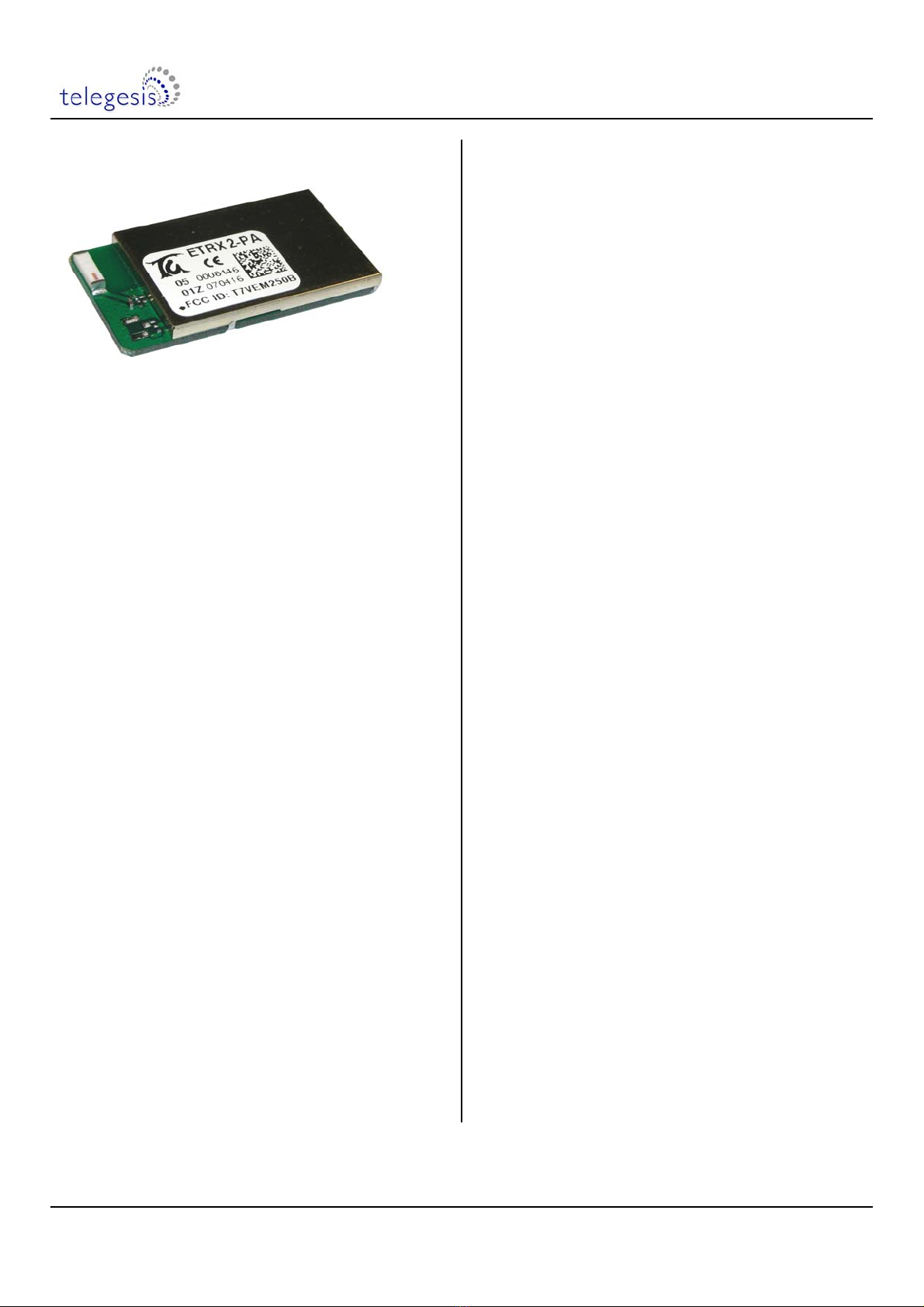
Image not shown actual size; enlarged to show detail.
The Telegesis ETRX2-PA module is a power
amplified 2.4GHz ISM band transceiver based on the
Ember EM250 single chip ZigBee®/IEEE802.15.4
solution. It has been designed to be integrated into
any device without the need for RF experience and
expertise. The form factor of the ETRX2-PA is
identical to the ETRX2, so either module can be
used depending on the range requirements of the
particular application. Utilizing the EmberZNet
meshing and self-healing stack, the ETRX2-PA
enables you to add powerful wireless networking
capability to your products and quickly bring them to
market. The module’s unique AT-style command line
interface allows you to quickly integrate meshing
radio technology without complex software
engineering.
Suggested Applications
•AMR – Automatic Meter Reading
•Wireless Alarms and Security
•Home/Building Automation
•Wireless Sensor Networks
•M2M Industrial Controls
•Future ZigBee®systems
•PC Peripherals
•IEEE 802.15.4 Systems
•Item Tracking
Development Kits
•Two complementary development kits consisting of
three or six modules and a single development board
with USB connectivity and I/O breakouts.
•AT-style software interface command dictionary can
be modified for high volume customers.
•Custom software development available upon
request.
Example AT-Style Commands
AT+BCAST Sends a Broadcast
AT+UCAST:<address> Sends a Unicast
AT+EN Establish PAN network
AT+JN Join any PAN
At power-up the last configuration is loaded from non
volatile S-Registers, which can eliminate the need for an
additional host controller.

ETRX2PA
©2009 Telegesis (UK) Ltd - 5 - ETRX2PA Product Manual (Rev 1.06)
1 Introduction
This document describes the Telegesis ETRX2-PA ZigBee® module which has been designed to
be integrated into another device and to provide a fast, simple and low cost wireless mesh
networking interface.
The Telegesis ETRX2-PA module is based on the Ember ZigBee® platform consisting of the single
chip EM250 combined with the ZigBee PRO compliant EmberZNet meshing stack. Integration into
a wide range of applications is made easy using a simple AT style command interface and
advanced hardware design.
The configurable functionality often allows the ETRX2-PA wireless meshing module to be used
without an additional host microcontroller saving even more integration time and costs. In addition
to the Telegesis AT Commandset, the ETRX2-PA can be used in with custom build firmware or the
Ember EZSP over UART protocol interface...
No RF experience or expertise is required to add this powerful wireless networking capability to
your products. The ETRX2-PA offers fast integration opportunities and the shortest possible time
to market for your product.
1.1 Hardware Description
The main building blocks of the ETRX2-PA are the single chip EM250 from Ember, a 24MHz
reference crystal and RF front-end circuitry optimized for best RF performance. With single ended
RF output, the module is available with integrated antenna or 50ΩU.FL coaxial connector or 50Ω
pad terminal on the bottom of the module.
The integrated antenna is a Johanson 2450AT43A100, and details of the radiation pattern etc are
available from their website [4].
Compared to the ETRX2, the ETRX2-PA module allows extended range of operation by means of
an integrated high efficiency power amplifier inserted in the Tx path.
A low loss LTCC band-pass filter for the 2.4GHz ISM band is added to both the Tx and Rx path.
As a result for Rx mode the immunity against interferers (for example operating at 1.8 GHz) is
improved compared to the standard ETRX2.
The ETRX2 is used for ZigBee® (www.zigbee.org)applications. If you wish to create your own
custom firmware, and not use the pre-loaded Telegesis AT-Command interface, you will need the
InSight toolchain, consisting of InSight Desktop™ together with a comprehensive integrated
development environment (IDE) and C-language compiler toolchain from Ember. The Ember
firmware is not suitable for an 802.15.4-only application that does not use the ZigBee layer.
As an alternative to the Telegesis R2xx and R3xx series AT Command interfaces, the ETRX2-PA
can also be supplied with Ember’s UART EZSP (Ember ZigBee Serial Protocol) firmware. Please
refer to the Ember EM260 manual for more information on the EZSP.
1.2 Hardware precautions
1.2.1 Unexpected start-up in bootloader mode
The bootloader which runs on the ETRX2 can be initiated with a firmware command, but it can also
be triggered in hardware. If the A/D2 input (pad 10) is pulled low during the boot-up of the module
it will enter the bootloader routine, so exercise caution when doing hardware design and ensure

ETRX2PA
©2009 Telegesis (UK) Ltd - 6 - ETRX2PA Product Manual (Rev 1.06)
that this pin is not grounded during start-up and reset or driven from an analogue voltage that may
be sensed as a logic 0. If unused the pad can be left floating and a pull-up is not required.
2 Product Approvals
The ETRX2 has been designed to meet all national regulations for world-wide use. In particular
the following certifications have been obtained:
2.1 FCC Approvals
The Telegesis ETRX2-PA and also the ETRX2HR-PA including the antennae listed in Table 1
complies with FCC CFR Part 15 (USA). The devices meet the requirements for modular
transmitter approval as detailed in the FCC public notice DA00.1407.transmitter.
This device complies with Part 15 of the FCC rules. Operation is subject to the following
two conditions: (1) this device may not cause harmful interference, and (2) this device must
accept any interference received, including interference that may cause undesired
operation.
FCC ID: T7VEM250B
This module complies with the USA SAR requirements and is not intended to be operated within
20cm of the body. The following statement must be included as a CAUTION statement in manuals
for OEM products to alert users on FCC RF exposure compliance:
“WARNING: To satisfy FCC RF exposure requirements for mobile transmitting devices, a
separation distance of 20cm or more should be maintained between the antenna of this
device and persons during operation. To ensure compliance, operations at closer
distances than this are not recommended.”
Item Part No. Manufacturer Type Gain
1 BKR2400 Embedded Antenna Design Ltd. ½ Wave Dipole 2 dBi
2 BT-Stubby (Straight) Embedded Antenna Design Ltd. Wire 0 dBi
2 BT-Stubby
(right-angle) Embedded Antenna Design Ltd. Wire 0 dBi
Table 1: Approved Antennae
While the applicant for a device into which the ETRX2-PA or ETRX2HR-PA (with an antenna listed
in Table 1) is installed is not required to obtain a new authorization for the module, this does not
preclude the possibility that some other form of authorization or testing may be required for the end
product.
The FCC requires the user to be notified that any changes or modifications made to this device
that are not expressly approved by Telegesis (UK) Ltd. may void the user's authority to operate the
equipment.
When using the ETRX2HR-PA with approved antennae, it is required to prevent end-users from
replacing them with non-approved ones.

ETRX2PA
©2009 Telegesis (UK) Ltd - 7 - ETRX2PA Product Manual (Rev 1.06)
2.1.1 FCC Labelling Requirements
When integrating the ETRX2-PA or ETRX2HR-PA into a product if must be ensured that the FCC
labelling requirements are met. This includes a clearly visible label on the outside of the finished
product specifying the Telegesis FCC identifier (FCC ID: T7VEM250B) as well as the notice
above. This exterior label can use wording such as “Contains Transmitter Module FCC ID:
T7VEM250B” or “Contains FCC ID: T7VEM250B” although any similar wording that expresses
the same meaning may be used.
2.2 European Certification
The ETRX2PA and ETRX2HR-PA are certified at a power level of 21.15mW e.i.r.p. (13.2dBm) to
the following standards:
•Radio: EN 300 328 v1.7.1 (10/2006)
•EMC: EN 301 489-17 v1.2.1 (08/2002)
•Safety: EN 60950-1:2006
The ETRX2HR-PA was tested with the antennae listed in Table 1.
0681EC-R&TTE Certificated
If the ETRX2 module is incorporated into an OEM product, the OEM product manufacturer must
ensure compliance of the final product to the European Harmonised EMC, and low voltage/safety
standards. A Declaration of Conformity must be issued for each of these standards and kept on
file as described in the R&TTE Directive. The final product must not exceed the specified power
ratings, antenna specifications and installation requirements as specified in this ETRX2 user
manual. If any of these specifications are exceeded in the final product then a submission must be
made to a notified body for compliance testing to all of the required standards.
The ‘CE’ marking must be applied to a visible location on any OEM product. For more information
please refer to http://ec.europa.eu/enterprise/faq/ce-mark.htm. Customers assume full
responsibility for learning and meeting the required guidelines for each country in their distribution
market.
Important Note: In Europe the regulations for the 2.4GHz frequency band are only harmonized for
devices with an e.i.r.p. of less than 10mW (10dBm). In the case of e.i.r.p. of more than 10mW the
manufacturer or his authorised representative established within the community or the person
responsible for placing the equipment on the market shall notify the national authority responsible
in the relevant Member State for spectrum management of the intention to place such equipment
on its national market. This notification shall be given no less than four weeks in advance of the
start of placing on the market.
Because of this Telegesis recommends that the user limit the output power to 10mW (10dBm) for
Europe to avoid having to deal with the local authorities for spectrum management of each
relevant member state.

ETRX2PA
©2009 Telegesis (UK) Ltd - 8 - ETRX2PA Product Manual (Rev 1.06)
2.3 Declarations of Conformity
Telegesis (UK) Ltd has issued Declarations of Conformity for the ETRX2 ZigBee® RF Modules,
which cover Radio Emissions, EMC and Safety. These documents are available from our website
or on request
2.4 IEEE 802.15.4
IEEE 802.15.4 is a standard for low data rate, wireless networks (raw bit-rate within a radio packet
of 250kbps @2.4GHz) which focuses on low cost, low duty cycle, long primary battery life
applications as well as mains-powered applications. It is the basis for the open ZigBee® Protocol.
2.5 The ZigBee® Protocol
The ZigBee® Protocol is a set of standards for wireless connectivity for use between any devices
over short to medium distances. The specification was originally ratified in December 2004, paving
the way for companies to start making low-power networks a reality.
ZigBee® uses an IEEE 802.15.4 radio specification running on the 2.4GHz band, plus three
additional layers for networking, security and applications. What makes the specification unique is
its use of a mesh network architecture which, in bucket chain style, passes data from one node to
the next until it lands at its destination. The network is self-healing and adapts its routing as link
quality changes or nodes move. Furthermore, nodes can be defined as End Devices which do not
act as routers, but can therefore be put into a low-power sleep state.
The enhanced version of the ZigBee® standard (or ZigBee® 2006) was released in December
2006, adding new features and improvements to the only global wireless communication standard
enabling the development of easily deployable low-cost, low-power, monitoring and control
products for homes, commercial buildings and industrial plant monitoring. In 2007 the ZigBee
Alliance produced the very latest edition of the standard including the PRO featureset which offers
advantages over earlier versions, including
•Truly self healing mesh networking
•Messages can now travel up to 30 hops
•Source-Routing for improved point to multipoint message transmission
•Improved security including Trust-Centre link keys
•New message types and options
Based on this latest standard, the Telegesis R3xx firmware for ZigBee PRO allows for
•Support for up to 4 external interrupts and 4 analogue inputs
•Nodes can be addressed by their EUI as well as their 16 bit NodeID
•Some level of interoperability with 3rd party ZigBee PRO compliant nodes
Please note that the R2xx and to some extent the Telegesis AT-Command line interpreter are
based on a private application profile and use the Ember meshing and self-healing stack, so
interoperability with wireless mesh networking solutions from other manufacturers is unlikely when
using this default firmware. For more information on ZigBee® compliance and the AT command
interface please refer to the latest AT command dictionary and the ETRX2 user guide.

ETRX2PA
©2009 Telegesis (UK) Ltd - 9 - ETRX2PA Product Manual (Rev 1.06)
3 Module Pinout
The ETRX2-PA is pin-compatible with the ETRX1, (NB: it has additional pins to the ETRX1). For
all new designs using either ETRX1 or ETRX2 it is recommended that you use the ETRX2 footprint
to ensure the option of future upgrading is guaranteed.
Figure 1: ETRX2 Module Pinout
The table below gives details about the 38 module pin signals for direct SMD soldering of the
ETRX2-PA to the application board. The pin numbers shown in brackets () are the related pins of
the EM250. In order to use the ETRX2-PA as a plug-in solution a Harwin 1.27mm pitch connector
can be fitted on the bottom of the ETRX2-PA (Harwin part number M50-3601042). Other
connectors that use the same footprint may also be used, such as a Samtec TFML-110-02-S-D.
All GND pads are connected within the module, but for best RF performance all of them should be
grounded externally.

ETRX2PA
©2009 Telegesis (UK) Ltd - 10 - ETRX2PA Product Manual (Rev 1.06)
ETRX2
Pad Function EM250 GPIO ETRX2
Harwin Pin
1 GND GND
2 Antenna
3 GND GND
4 I/O9 GPIO 0 (21) 1
5 Vreg {1} 2
6 GND GND 3
7 Vcc 10
8 GND GND 3
9 A/D1 GPIO 4 (26) 4
10 A/D2 GPIO 5 (27) 5
11 I/O7 GPIO 3 (25) 6
12 I/O6 GPIO 2 (24) 7
13 I/O5 GPIO 1 (22) 8
14 I/O4 or RTS {3} GPIO 12 (20) 9
15 GND GND
16 SIF CLK SIF CLK
17 SIF MISO SIF MISO
18 SIF MOSI SIF MOSI
19 SIF LOADB SIF LOADB
20 GND GND
21 I/O8 GPIO 6 (29) 11
22 I/O2 or CTS {3} GPIO 11 (19) 12
23 I/O3 GPIO 13 (43) 13
24 Reset (13) 14
25 I/O1 GPIO 14 (42) 15
26 I/O0 GPIO 8 (31) 16
27 TXD GPIO 9 (32) 18
28 RXD GPIO 10 (33) 17
29 GND GND 3
30 I/O10 GPIO 15 (41) 19
31 I/O11 GPIO 16 (40) 20
32 GND GND
33 VCONT {2} n/a
34 GND GND
35 GND GND
36 GND GND
37 GND GND
38 N/C GPIO 7 (30)
Table 2. Pin Information
Notes:
{1} Where the onboard regulator option is mounted this pin is connected to the output voltage of the
onboard regulator option and NOT to the output voltage VREG_OUT of the EM250
{2} VCONT is the internal amplifier gain control voltage, resistive external loading to ground can reduce
the amplifier gain and therefore lower the maximum available module Tx output power. For most of
the applications this pin is NOT connected and the amplifier is working at maximum gain.
Controlling the maximum output Power can also be achieved in software.
{3} RTS/CTS handshaking is selectable in firmware. See the AT Command Manual.

ETRX2PA
©2009 Telegesis (UK) Ltd - 11 - ETRX2PA Product Manual (Rev 1.06)
4 Hardware Description
24MHz
32,768kHz
(optional)
EM250
RF transceiver 2.4GHz
16-bit XAP16b uC
128kB flash / 5k RAM
GPIO0
GPIO16 I / O
programming
4SIF
LDO
or
DC
converter
(optional)
VBATVBAT VREG
RESET RESET
BALUN
integrated
antenna
Pad 2
U.FL socket
rf
terminal
selection,
filtering and
matching
circuitry
LDO
1,8Vdc
Tx
Rx
BALUN
Rx/Tx
switch
PA
Figure 2: Hardware Diagram
4.1 Hardware Options
Please contact the manufacturer if any of the options described below could be useful in your
product design. Please note that to include these options a high order quantity is required and
they are not available as standard products.
4.1.1 On-board DC Regulator
Although the EM250 already contains an internal LDO regulator, the module can be supplied with
an additional integrated onboard LDO regulator or DC/DC converter. Some applications could
benefit from this additional regulator in instances where:
(1) Further extension of the input voltage range is required
(2) Extended battery life is obtained by replacing the regulator within the EM250 with a special
ultra-low quiescent current regulator
(3) Operation is required using very noisy power supplies
Two different types of regulators are available, a linear low dropout (LDO) type or a high efficiency
switched buck regulator. Depending on the power supply conditions of the application the
optimum regulator can be selected.
4.1.2 On-board Reference Crystal
A second option which is available is an on board 32.768kHz crystal reference. This option can be
provided for applications which require a high precision reference clock.
4.1.3 RF output pad
Thirdly, the RF output can be connected to pad 2 for routing on to the underlying circuit board.
There is then no ceramic antenna nor U.FL connector.

ETRX2PA
©2009 Telegesis (UK) Ltd - 12 - ETRX2PA Product Manual (Rev 1.06)
5 Hardware Interface
All I/O pins of the EM250 are accessible on the module’s pads. The pre-loaded Telegesis AT
Command Interface defines those I/Os as described below. Please refer to the Command
Dictionary and to the User Guide to learn more about the pre-loaded firmware. When developing
custom firmware all pins can be utilised as described in the EM250 datasheet.
ADC
The module has up to four analogue inputs. Readings with reference to the internal 1.2V
reference voltage can be made locally as well as over the air.
I/O
Pins I/O11 down to I/O0 are bi-directional I/O ports which can be controlled locally as well as
remotely by accessing local as well as remote S-registers. The functionality of the I/Os can be
controlled using three single 16-bit registers representing the data direction, the output buffer and
the input buffer. With the R3xx series of firmware it is now also possible to select internal pull-ups
or pull-downs for each individual I/O.
UART
The AT style command interpreter can be accessed via the TXD and RXD pins. The ETRX2-PA
can buffer up to 128 bytes of incoming data in a software FIFO buffer and uses XON/XOFF or
hardware flow control. See [2] for more information about the built-in UART.
Interrupt
Up to 4 I/Os can trigger user definable actions. User configurable edges can cause interrupts if
this function is enabled in the S-Registers.
Reset
Pulling the reset pin low will cause the module to restart. An external pull-up is not required, but
can be added for use in a very noisy environment.
PWM
I/O3 can alternatively act as a special function pin which can generate output waveforms up to
12MHz or act as a PWM. This functionality can be controlled locally as well as remotely by
accessing local as well as remote S-registers.
Antenna
Matching is provided to match the radio to the integrated antenna or to an optional external general
purpose 2.4GHz antenna. The on board antenna is supplied by Johanson. For full data on the
Johanson antenna please refer to [4].
Power
The module is able to operate from 3.5V down to 2.7V which makes it ideally suited for battery-
powered applications.
SIF
Interface for programming and real-time debugging the EM250.

ETRX2PA
©2009 Telegesis (UK) Ltd - 13 - ETRX2PA Product Manual (Rev 1.06)
6 Firmware Description
The modules are pre-loaded with a standalone bootloader which supports over-the-air bootloading
as well as serial bootloading of new firmware.
In order to enter the standalone bootloader using a hardware trigger pull A/D2 (GPIO5) to ground
and power-cycle the module. To avoid entering the standalone bootloader unintentionally make
sure not to pull this pin down during boot-up unless the resistance to ground is >10kΩ. (A pull-up
is not required).
In addition to the standalone bootloader the modules also contain the current release of the
Telegesis AT-style command interface as described in the Telegesis AT command dictionary and
the Telegesis user guide. Check www.telegesis.com for updates. Each module comes with a
unique 64-bit 802.15.4 identifier which is stored in non-volatile memory. The commands and
responses pass through the serial port of the ETRX2PA as ASCII text, so a simple terminal
application will usually suffice. We provide Telegesis Terminal but it is not an essential feature.
The pre-loaded AT-style command interface firmware is based on the latest EmberZNet meshing
stack which implements routers/coordinators as well as (sleepy) end devices. [End devices have
no routing responsibility and therefore are allowed to go to sleep, whilst still being able to send and
receive messages via a parent router. In addition to a classical (sleepy) end device the module
firmware also supports mobile (sleepy) end devices capable of changing their parent quickly
whenever they change their position within the network.]
A router is typically a mains powered device whilst a sleepy end device (SED) can be battery
powered.
The module is also able to act as a PAN coordinator through external host control. The AT style
command line supplies all the tools required to set up and manage a wireless mesh network by
allowing easy access to the low-level functionality of the stack.
The ETRX2 firmware uses the meshing and self healing EmberZNet PRO stack to overcome many
of the limitations of the tree network topology of the ZigBee® 2006 stack. Following further
evolution of the ZigBee® mesh networking specification, Telegesis also offer firmware that
implements the PRO feature set of ZigBee 2007.
The Telegesis firmware also allows low-level access to physical parameters such as channel and
power level. Parameters that define the functionality of the ETRX2-PA module and also allow
standalone functionality are saved in non-volatile memory organised in so-called S-Registers. The
SPI and I2C buses are not supported by the current firmware release, but can be used with custom
firmware.
As a third option as opposed to using the Telegesis AT command interface or developing custom
firmware, the Ember EZSP UART interface can be provided to allow ZigBee® application
development using a host controller driven binary protocol. For more information on the EZSP
interface please refer to the Ember EM260 datasheet.
6.1 Custom Firmware
For high volume customers the firmware can be customised on request. Customers can use the
ETRX2-PA module as hardware only and develop their own firmware based on the EmberZNet
stack. In order to develop custom firmware Insight Desktop™ is required together with a
comprehensive integrated development environment (IDE) and C-language compiler toolchain
from Ember.

ETRX2PA
©2009 Telegesis (UK) Ltd - 14 - ETRX2PA Product Manual (Rev 1.06)
6.2 Software Interface
Using the default firmware the ETRX2-PA is controlled using a simple AT-style command interface
and (mostly) non-volatile S-Registers. In order to get a full listing of all the available AT-
Commands, please refer to the AT command dictionary document which corresponds to the
firmware revision you intend to use.
In addition to the command dictionary there are user guides explaining the features of the firmware
in more detail. If you need to find out which firmware resides on your module simply type “ATI”
followed by a carriage return and you will be prompted with the module’s manufacturing
information.
The Development Kit manual describes how to upgrade the firmware either via a serial link or over
the air.

ETRX2PA
©2009 Telegesis (UK) Ltd - 15 - ETRX2PA Product Manual (Rev 1.06)
7 Absolute Maximum Ratings
Supply: 3.5V
Inputs: -0.3V to Vcc+0.3V
Operating temperature: -40 to 85°C
No. Item Symbol Absolute Maximum Ratings Unit
1 Supply voltage VBAT -0.1 to +3.5 Vdc
2
Voltage on any I/O[11:0],
SIF_CLK, SIF_MISO, SIF_MOSI,
SIF_LOADB, RESET
Vin -0.3 to VBAT+0.3 Vdc
3 Voltage applied to Vreg Vreg -0.3 to 2.0 Vdc
4 Storage temperature range Tstg -40 to +105 °C
5 Operating temperature range Top -40 to +85 °C
6 Input RF level Pmax 0 dBm
7
ESD on any pin (1) according to
Human Body Model (HBM) circuit
description
VTHHBM ±2 kV
8 Reflow temperature TDeath Please refer to chapter 13 °C
Table 3. Absolute Maximum Ratings
Notes:
(1) Input must be current limited to the value specified.
The absolute maximum ratings given above should under no circumstances be violated.
Exceeding one or more of the limiting values may cause permanent damage to the device.
Caution! ESD sensitive device. Precautions should be used when handling the device
in order to prevent permanent damage.
8 Operating Conditions
Please Note: The firmware of the ETRX2 series and the ETRX2-PA series is identical, therefore
when talking about power settings in the following chapters, the actual output power out of the on
board EM250 is described, rather than the power amplified output out of the module. For the
relationship between EM250 power settings and module output power please relate to chapter
11.1 of this document. When developing custom firmware the output power settings described in
this document relate directly to the EM250 power settings accessible via the Ember stack API.

ETRX2PA
©2009 Telegesis (UK) Ltd - 16 - ETRX2PA Product Manual (Rev 1.06)
No. Item Condition /
Remark Symbol Value Unit
Min Typ Max
1 Supply voltage The typical value
is recommended VDD 2.7 3.3 3.5 Vdc
2 RF Input Frequency fC2405 2480 MHz
3 RF Input Power pIN 0 dBm
4 EM250 Tx power mode
setting NORMAL MODE or BOOST MODE(1) and
external PA
5 EM250 Tx output power
setting Channels 12-25 pOUTSET -43 +3 dBm
6 EM250 Tx output power
setting(2) Channel 11 pOUTSET -43 -3 dBm
7 EM250 Tx output power
setting(2) Channel 26 pOUTSET -43 -14 dBm
8
Typical module output
power corresponding to
Item 5. For more details
see part 11.1.
Channels 12-25
NORMAL MODE
BOOST MODE
pOUT
-22
-21
+17.5
+18.5
dBm
9 Tx Duty Cycle
Maximum output
power set and 0dBi
Antenna (3)
10 %
10 Logic Input Voltage Low VIL 0 0.2x
VBAT V
11 Logic Input Voltage High VIH 0.8x
VBAT VBAT V
12 Voltage Level on any of
the A/D Inputs VA/D 1.2 V
13 SPI clock rate fSPI 12 MHz
14 Operating temperature
range Top -40 +85 °C
Table 4. Operating Conditions
The conditions for compliance are:
(1) BOOST MODE is allowed with some restrictions:
In order to stay within the output power limits of 20dBm and -30dBm PSD mask
absolute (IEEE802.15.4) the power setting value is limited to 0dBm, the maximum
supply voltage is limited to 3.3V and the operating temperature is limited to
temperatures above 0°C.
(2) On the lowest channel 11 (2405 MHz) and the highest channel 26 (2480 MHz) the
maximum allowed output power settings are limited to the maximum values stated
above in order to not exceed the spectral power limits at the 2.4GHz ISM band edges
under extreme conditions as stated in part 4.3.3 “Frequency Range” of [1]
(3) With these settings and duty cycles below 10% the limits for “Maximum Spectral Output
Power density” according to part 4.3.2 of [1] are not exceeded. For lower antenna gain
and/or lower TX output power the duty cycle may be increased according to the
formula in [1].
Please Note: The average current consumption during operation is dependent on the firmware
and the network load, therefore these figures are given in the command dictionary of the
respective firmware.

ETRX2PA
©2009 Telegesis (UK) Ltd - 17 - ETRX2PA Product Manual (Rev 1.06)
9 DC Electrical Characteristics
VBAT = 3.3V, TAMB = 25°C, NORMAL MODE unless otherwise stated
No. Item Condition /
Remark Symbol Value Unit
Min Typ Max
1 Module supply voltage
VBAT VBAT 2.7 3.3 3.5 Vdc
2 Internal regulated core
voltage
connected to
Vreg pin 5 (1) VCORE 1.7 1.8 1.9 Vdc
3
Quiescent current,
excluding
internal RC oscillator
10kΩpull-down at
SIF_MOSI pin ISLEEP 0.8 3.0 µA
4
Quiescent current,
including
32.768kHz oscillator
10kΩpull-down at
SIF_MOSI pin ISLEEP 1.5 3.5 µA
5 Transmit current
consumption
at +17.5dBm
module output
power
ITXVBAT 106 120 mA
6
Transmit Current
consumption
BOOST MODE
at +18.5dBm
module output
power
ITXVBAT 121 130 mA
7 Transmit current
consumption
at +10dBm
module output
power
ITXVBAT 63 mA
8 Transmit current
consumption
at +0dBm module
output power ITXVBAT 56 mA
9 Receive current
consumption total IRX 37 mA
10 External load on internal
regulated core voltage
connected to
Vreg pin 5 (1) IREG_OUT 2 mA
11 Input voltage for logic 0 VIL 0 0.2xVBAT Vdc
12 input voltage for logic 1 VIH 0.8xVBAT VBAT Vdc
13 Input current for logic 0 IIL -0.5 µA
14 input current for logic 1 IIH 0.5 µA
15 input pull-up resistor
value RIPU 30 kΩ
16 input pull-down resistor
value RIPD 30 kΩ
17 Output voltage for logic 0 VOL 0 0.18xVBAT Vdc
18 Output voltage for logic 1 VOH 0.82xVBAT VBAT Vdc
19 Output source current
(standard current pad) IOHS 4 mA
20 Output sink current
(standard current pad) IOLS 4 mA
21
Output source current
(high current pad: I/O3,
I/O1, I/O10, I/O11 )
IOHH 8 mA
22
Output sink current (high
current pad: I/O3, I/O1,
I/O10, I/O11)
IOLH 8 mA
23 Total output current
for I/O pads IOH + IOL 40 mA
Table 5. DC Electrical Characteristics
Notes: (1) For more information about the internal regulated core voltage refer to part 5.7 in [2]. As the
internal regulated core voltage at VREG mainly feeds circuitry on ETRX2-PA, the VREG module pin may only
be slightly loaded and without feeding noise to VREG. VREG is not available in Power Mode 3 (see the AT
Command Manual for details of power modes).
Where the dc regulator option is mounted VREG is connected to the regulator option output instead and the
internal regulated core voltage is not accessible.

ETRX2PA
©2009 Telegesis (UK) Ltd - 18 - ETRX2PA Product Manual (Rev 1.06)
10 A/D Converter Characteristics
No. Item
1 A/D characteristics refer to datasheet EM250 part 5.5 ADC Module
2 A/D timing/performance characteristics refer to datasheet EM250 part 5.5 ADC Module
3 Reference Voltage 1.2V
4 Maximum Input Voltage 1.2V
Table 6. A/D Converter Characteristics
Note: If a voltage higher than 1.2V is applied to any of the ADC inputs, the readings on the
other ADCs will be incorrect.
11 AC Electrical Characteristics
VBAT = 3.3V, TAMB = 25°C, NORMAL MODE measured at 50Ωterminal load connected to the U.FL socket
No. Receiver Value Unit
Min Typ Max
1 Sensitivity for 1% Packet Error Rate (PER) -92 -96 - dBm
2 Sensitivity for 1% Packet Error Rate (PER) BOOST MODE -93 -97 - dBm
3 Saturation (maximum input level for correct operation, low gain) 0 4 - dBm
4 Adjacent Channel Rejection
(1% PER and desired signal –82dBm acc. to [1]) 30 dB
5 Alternate Channel Rejection
(1% PER and desired signal –82dBm acc. to [1]) 40 dB
6 Channel Rejection for all other channels
(1% PER and desired signal –82dBm acc. to [1]) 40 dB
7 802.11g rejection centred at +12MHz or –13MHz
(1% PER and desired signal –82dBm acc. to [1]) 40 dB
8 Co-channel rejection
(1% PER and desired signal –82dBm acc. to [1]) -6 dBc
9 RF frontend filter attenuation for interferers in the range 1710-
1910MHz 30 dB
10 Relative frequency error
(2x40ppm required by [1]) -80 80 ppm
11 Relative timing error
(2x40ppm required by [1]) -80 80 ppm
12 Linear RSSI range 40 50 dB
13 Spurious Emissions <1GHz - -74 -57 dBm
14 Spurious Emissions >1GHz - -60 -47 dBm

ETRX2PA
©2009 Telegesis (UK) Ltd - 19 - ETRX2PA Product Manual (Rev 1.06)
No. Receiver Value Unit
Min Typ Max
15
Output power at highest power setting
normal mode
NORMAL MODE
BOOST MODE
14
15
17.5
18.5 20 dBm
16 Output power at power setting -20dBm 0 dBm
17 Output power at lowest power setting -22 dBm
18 Error vector magnitude as per IEEE802.15.4 10 35 %
19 Carrier frequency error -40 40 ppm
20 PSD mask relative
3.5MHz distance from carrier -20 -36 dB
21 PSD mask absolute
3.5MHz distance from carrier -30 TBD dBm
22 2nd harmonic at highest power setting - -60 -30 dBm
23 3rd harmonic at highest power setting - -52 -30 dBm
24 Spurious Emissions <1GHz - -60 -36 dBm
25 Spurious Emissions >1GHz - -57 -30 dBm
Table 7. AC Electrical Characteristics
Notes:
(1) at pin 38 RF or U.FL socket, for all channels number 11,12,..., 26 according to ref [1]
No. Standby Limit Unit
Min Typ Max
26 Spurious Emissions <1GHz - -66 -57 dBm
27 Spurious Emissions >1GHz - -66 -47 dBm
Table 8. Standby Spurious Emissions
No. Synthesiser Characteristics Limit Unit
Min Typ Max
29 Lock time from off state, with correct VCO DAC settings 100 µs
30 Relock time, channel change or Rx/Tx turnaround 100 µs
Table 9. Synthesiser Characteristics
No. Power On Reset (POR) Specifications Limit Unit
Min Typ Max
31 VBAT POR release 1.0 1.2 1.4 Vdc
32 VBAT POR assert 0.5 0.6 0.7 Vdc
33 VCORE POR release 1.35 1.5 1.65 Vdc
34 VCORE POR hysteresis 0.08 0.1 0.12 Vdc
Table 10. Power On Reset Specifications

ETRX2PA
©2009 Telegesis (UK) Ltd - 20 - ETRX2PA Product Manual (Rev 1.06)
11.1 TX Power Characteristics
The diagrams below show the typical output power and module current in dependency on module
supply voltage and EM250 power setting in NORMAL MODE.
Output power vs power setting
-30
-25
-20
-15
-10
-5
0
5
10
15
20
-50 -40 -30 -20 -10 0 10
power setting dBm
output power dBm
2.7
3
3.3
3.5
Figure 3. Output Power vs. Power Setting
Module current vs power setting
0
20
40
60
80
100
120
-50-40-30-20-10 0 10
power setting dBm
current mA
2.7
3
3.3
3.5
Figure 4. Module Current vs. Power Setting
Please Note: The power setting is the setting of the EM250’s output power (before amplification). This setting is used by
all firmware running on the ETRX2-PA.
Table of contents
Other Telegesis Control Unit manuals


Popular Control Unit manuals by other brands


Wildlife Acoustics
Wildlife Acoustics Echo Meter Touch 2 manual

Armstrong
Armstrong DRV40 manual

Watts
Watts 979GD-15 Installation, operation and maintenance

Blonder tongue
Blonder tongue DAP Series instruction manual

VersaLogic
VersaLogic VersaFlap H.25 Manual instructions

Fike
Fike FIK-CR-6 Installation and maintenance instructions

Bray
Bray TRI LOK Operation and maintenance manual

Jonix
Jonix VMC Use and maintenance manual

Xanavi Informatics Corporation
Xanavi Informatics Corporation HJZ0093 user manual

Walther
Walther SMS-07 Assembly instructions

FlexRadio
FlexRadio FLEX-6000 Signature Series user guide

Ingersoll-Rand
Ingersoll-Rand Dor-O-Matic 96000 Series installation instructions