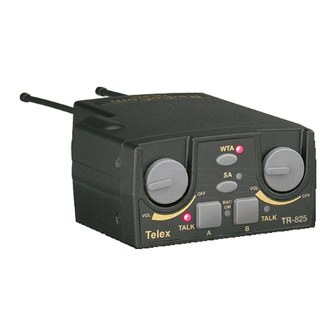
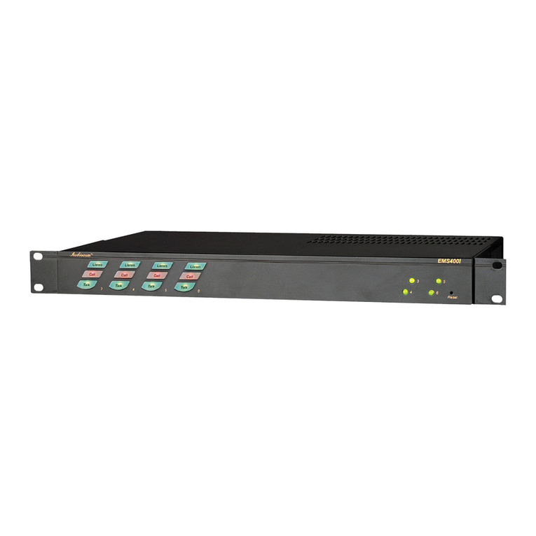
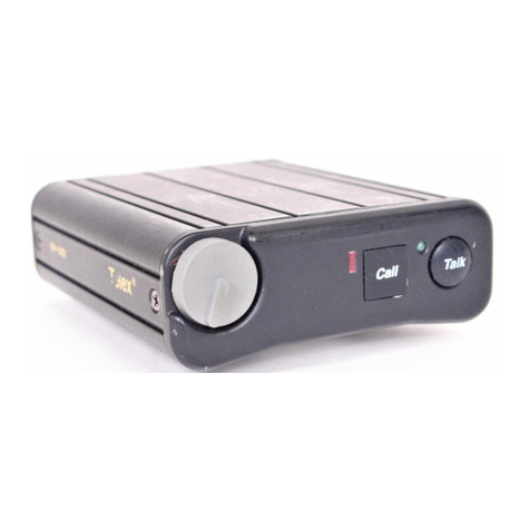
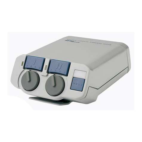
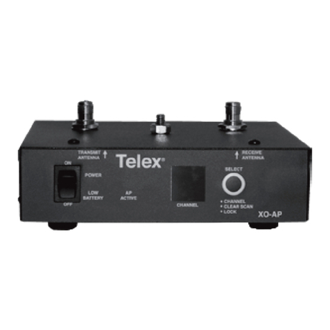
Telex Radiocom BTR-200 Series User manual

-----------------------~--~--_._
_-
_.
-
ca
::J
c:
ca
><
.:2
W~
....I
-s;:
Wi..
....
~
Ci
c)
mm",,~~
:E
w
..J I-en
<t
enW
Z
>-
enD:
Q(/):Em
l~iDD
~
fa
80
a~~~
~
d
a:
~
lll~L
...
lOO~
it
3=
~
ttl
.-"\
j
€l
X
W
.J
W
I-

()
Table
of
Contents
Page
Chapter
1
General Description
1-1
Specifications BTR-200
1-1
Controls and Connections 1-2
Front Panel 1-2
Rear Panel 1-5
Chapter
2 - Identification
of
Circuit
Board
Revision
and
Version
Audio Boards ......•.................................................................................................................................... 2-1
Receive Board 2-2
Transmit Board 2-3
Chapter
3 - Transmit, Receive &Audio Circuit Boards
BTR-200 Instrument Disassembly 3-1
Transmit Board 3-2
Circuit Descdption 3-2
Alignment Procedure :3-2
Voltage Tables -Transmit Board (878521) 3-3
PCB Transmit Assembly (878521-*)(palts List) ;3-7
Receive Board 3-9
Circuit Descdption (PCB 70714000) 3-9
Circuit Descdption (PCB 750309)) 3-9
Alignment Procedure 3-10
Receive Board (70714000) 3-10
Equipment Required 3-10
Receive Board (750309) 3-11
Equipment Required 3-11
Voltage Tables -Receive Board (70714000) 3-14
Voltage Tables -Receive Board (750309) 3-15
PCB Receive Assembly 878522* (Parts List) 3-21
PCB Receive Assembly 878662* (Parts List) 3-24
Audio Board ,
::
3-27
Audio Board Circuit Description 3-27
Receive Expanders 3-27
MicrophoneAmplifier 3-27
Auxiliary InputAmplifier 3-27
Intercom Driver 3-27
Intercom Input. 3-28
Headset and SpeakerAmplifiers 3-28
Transmit'Mixer and Filter 3-28
Auxiliary Output· 3-28
Remote Transmit Circuit 3-28
Power
Supply 3-28
Alignment Procedure 3-29
Equipment Required 3-29
-i-

Page
Chapter
3·
Transmit, Receive &Audio CircuitBoards (Continued)
Audio Board Continued
PCB Audio Assembly (878520) Versions 1thru 6(Parts List) 3-45
Display Board 3-48
PCB Display 878519 (Parts Lists) 3-48
List
of
Illustrations
Figure
1
2
3
4
5
6
7
8
9
10
II
12
13
14
15
16
17A
17B
18
19
20
21
22
23
24
25
26
27
28
29
30
31
32
33
34
Description Page
Headset XLR Connector Wiring 1-2
Front Panel-BTR200
1-3
Rear Panel -BTR-200 1-4
Location
of
Rev Level for Versions 1and 2(Audio Board)
2-1
Location
of
Rev Level for Versions 3
thlU
6(Audio Board)
2-1
Location
of
Rev Level for Versions Iand 2(Receive Board) 2-2
Location
of
Rev Level for Versions Iand 2(Transmit Board) 2-3
Exploded View -BTR-200 2-4
Transmit Board Component Layout (Foil Side) 3-4
Transmit Board Component Layout (Component Side) 3-4
Schematic Diagram Transmit Board -Version 13-5
Schematic Diagram Transmit Board -Version 23-6
Schematic Diagram Receive Board 3-16
Receive Board Component Layout (Component Side)
Versions Iand 2(70714000) 3-17
Schematic Diagram Receive Board Version 2(750309) 3-18
Receive Board Component Layout (Component Side) Version
1..
3-19
Receive Board Component Layout (Foil Side) 3-19
Receive Board Component Layout (Component Side) Version 2(750309) 3-19
Schematic Diagram Receive Board Version I(750309) 3-20
Block Diagram Versions 1and 23-31
Block Diagram Versions 3
thlU
6 : 3-32
Audio Board Component Layout (Component Side) Versions land 23-33
Audio Board Component Layout (Foil Sde) 3-34
Schematic Diagram Audio Board Version I3-35
Schematic Diagram Audio Board Version 23-36
Details
of
Board Differences Between Versions Iand 23-37
Details
of
Board Difference
in
Versions 3, 4,
5,
and 63-38
Audio Board Component Layout (Component Side) Version 6
with Detailed Areas Showing Differences of Versions
3,4,5,
and 63-39
Audio Board Component Layout (Foil Side) Version 63-40
Schematic Diagram Audio Board Version 33-41
Schematic Diagram Audio Board Version 43-42
Schematic Diagram Audio Board Version 53-43
Schematic Diagram Audio Board Version 63-44
Display Board Component Layout (Foil Side) 3-48
Display Board Component Layout (Component Side) 3-48
-11-

CHAPTER 1
: -
')
GENERAL
DESCRIPTION
The BTR-200 is abase station which communi-
cates with up to four portable units simultaneously,
in
full duplex.
It
may be used alone with aheadset
or
interfaced
to
other
equipment
such
as a
hardwired intercom system.
n
1-1

CONTROLS
and
CONNECTIONS
FRONT
PANEL (Refer to Figure 2)
Power
ON/OFF
Switch: Push this switch once
to
turn power ON; push it again
to
turn the power
OFF.
Power
ON
Indicator:
The Power ON Indicator is
illuminated when the Power ON/OFF Switch is
pushed in the
ON
Position. It remains illuminated
while the Transceiver is on.
Local
Headset
Connector: 4Pin XLR Connector
for InputJOutput. The headset jack will accept 6
different Telex Model Headsets. Compatible with
otherintercom headsets with four pin XLRconnec-
tors that are wired as shown in Figure
1.
MICROPHONE
GROUND
BALANCED
AUDIO
OUT
MICROPHONE
AUDIO
Figure 1
Headset
XLR
ConnectorWiring
1-2
Local Headset Volume: Adjusts volume
to
Local
Headset. DOES NOT AFFECT MICROPHONE
GAIN.
Mic
On-Push-to-Talk/Lock-to-Talk
Switch:
Enables the local headset microphone audio func-
tion. NOTE: DOES NOT control base station RF
transmit.
Local
Push-to-Talk
Indicator:
Will
be
il-
luminated whenever the talk function is on.
Local Microphone
Gain
Control
and
Over-
modulation Indicator: Ascrewddver adjustable
control is provided
to
control the input level ofthe
local headset mic. This input is protected
from
overloads by means of again compressor whose
operation
is
signaled by the gain LED indicator.
Portable
EnableSwitches
and
Indicators: When
in the
"IN"
position, the Enable switches allow the
user ofthe conesponding portable unit
to
be heard
by others connected
to
the system. When
in
the
"OUT" position, the respective portable will
be
muted, but this portable will still be able
to
hear
all
other selected remotes and interfaces. The in-
dicators normally show the presence
of
aportable
transceiver in use
on
the channel corresponding
to
that indicator.

INTERCOM INDICATOR 27160-8-00I-A
LOCAL MIC
OVE
RMODULATION
INDICATOR
LOCAL MIC GAIN CONTROL
LOCAL
PUSH-TO-TALK
INDICATOR
MIC
ON
PUSIH-lO-TALKI
LOCK-TO-TALK SWITCH
PORTABLE CARRIER INDICATORS I
I
I
~OCAL
HEADSET VOLUME
I
i
AUXILIARY
ENABLE
INDICATOR
ENABLE SWITCHES
TO
RECEIVE
PORTABLE
TRANSMITTERS
I.-.--~
Portabte
Station
Connect--
AUXILIARY
LEVEL
CONTROL
AUXILIARY
ENABLE
SWITCH
INTERCOM LEVEL CONTROL
INTERCOM
ENABLE
SWITCH
POWER
ON
INDICATOR
Headset
8TR-200
1I
.LOCAL HEADSET CONNECTOR
Figure 2
Front
Panel-BTR200
1-3

27160-B-002-A
AUXILI
ARY
OUTPUT
CONNECTOR RECEIVE ANTENNA CONNECTOR
A~'~
300
rnA
-------
POWER JACK
o
Power
SPEAKER GAIN CONTROL
TELEX
COMMUNICA
TtONS.
INC.
Fex
1.0.
850BTR-200
MADE
IN
U.S.A.
Jack
CO
G~
LSpeaker-l
INTERCOM CONNECTORS
o
Intercom
Input
Transmit
1
TRANSMITTER
SWITCH
Headset
Mic
r"=-h
r~l
Oyn
fit
Cant
Off
Remote
HEADSET MIC
SELECT
SWITCH
AUXILJARY INPUT CONNECTOR
o
TRANSM
IT
ANTENNA
CONNECTOR
Transmit
Anteflna
SPEAKER
/
LOCAL
MONITOR
(8
n
MIN.)
Figure 3
Rear
Panel BTR-200
1-4

Ext
Intercom Switch, Level Control,
and
In-
dicator: This switch enables the wired intercom
interface when "IN", and disables it when "OUT".
For
RTS
intercoms, the "IN" position is channel A
and the "OUT" position ischannelB. Ascrewdriver
adjustable control is provided to control the input
level
of
the wired intercom.
Auxiliary Audio
Enable
Switch, Level Control,
and
Indicator:
Theswitchenablesand disables the
Auxiliary intelface when "IN" and "OUT", respec-
tively. The function
of
the level control here is the
same as that described for the intercom.
REAR
PANEL (Refer to Figure 3)
(j
Transmit
Antenna
Connector: Connect5/8-wave
antenna(supplied)
to
this connector. Antennacolor
should match connector dot
on
BTR-200.
Receive
Antenna
Connector: Connect 5/S-wave
antenna (supplied)
to
this connector. Antennacolor
should match connector dot
on
BTR-200.
Transmit
Switch: Slide switch that allows the
operator
to
select one
of
three transmit modes.
In
the "OFF" position, the transmitter is always off.
This mode may be used
if
the base is functioning
solely
as
amonitor. In the "CONT" position, the
transmitter is always on. This continuous mode is
recommended over the "REMOTE" mode. In the
"REMOTE" position, the transmitter is enabled
only when one or more portables are active.
Headset Microphone Select Switch: This switch
allows the user to select either
an
Electret
or
Dynamic microphone. This switch
i~
factory preset
to
DYN Position.
NOTE: All Telex headsets that are used with this
intercom are dynamic type microphones.
Intercom
Connectors: Connections to interface
the BTR-200 with awired intercom system.
Auxiliary
Output/Input
Connectors:
Can
be
used for 2-way (four wire) input and output to the
BTR-200 or as asimplex input or output. Typical
usesare 4wire low level intercoms, tape recorders,
public address inputs or outputs, orwhen operating
two BTR-200 units simultaneously.
Power
Jack:
Forexternal AC wall supply adaptor
(supplied) or any filtered 12 to 14 VDC/300 rnA
source, or 13.0
VAC
RMS/300 rnA source.
Speaker
Jack:
Allows the user to connect an ex-
ternal speaker
(8
ohms minimum)
to
the unit.
Speaker
Gain
Control: Screwdriver adjustable.
Adjust the gain control clockwise to increase
speaker gain
or
counterclockwise
to
decrease
speaker gain.
NOTE: Leave setting counterclockwise
if
no
speaker is attached.
1-511-6
Blank

CHAPTER 2
IDENTIFICATION
OF
CIRCUIT BOARD
REVISION AND VERSION
Version 1and 2use Rev Acircuit boards. The
location for the Rev letteris shown below. Version
2contains asmall circuit board with aswitch. See
Figure 4.
AUDIO BOARDS
This board is installed in the holes for C124 and
C125 (see below). Version 1does not have this
switchboard. For Rev C and higher, the location
for the Rev letteris shown in Figure 5.
AUDIO BOARD
RECEIVE BOARD
LOCATION
OF
SWITCHBOARD
70723-000 REV ACOMP
"'-.
••• _
r--------.
:I.
•
.2"!!2";!!.'!!!.I!.E!..~~_:
....
__
..
~---~_.:
o
Figure 4
Location
of
Rev Level for Versions 1
and
2
REV LEVEL LOCATED
.--
UNDER TRANSMIT
BOARD
70723-000 REV C
AUDIO BOARD
c. .
a:
IUI
«I
if
0I0I
I3I
!Xl
I&I
l-
'"
I
:E
L_
en
z
«
a:
I-
UII
Figure 5
Location
of
Rev Level for Versions 3
thru
6
2-1

Rev Cboards can be either Verion 3or 4. The
differences are all parts values: Rev Dboards are all version 5.
Rev Eboards are all version
6.
Rev Bwas not produced.
750309 COMP REV A
Version
RIOI
RI03
Rl25
Rl30
Rl31
Rl32
Rl33
Rl54
Rl62 Rl68
Rl70
Cl33
382K 82K 6.2K 1.5K 1.5K 1.5K 1.5K 5.6K
9.lK
68K
68K
lO~F
4
200K
200K
4.7K
4.7K 4.7K 4.7K 4.7 8.2K 3.9K 15K 10K
22~F
RECEIVE
BOARD
The
BTR-200
uses one
of
two receive boards.
Figure
6
Location
of
Rev Level
for
Versions 1
and
2
Early production units came with 70714000, and
750309 was installed in later units. 70714000
came in two versions that differed slightly (See
table below):
Version 2was built only with Rev Cboards.
Version 1was built with Rev A, B, or Cboards.
Thedifferentrevisionson this board were manufac-
turing changes that did not change the schematic.
750309 Rev Aboards are version
1.
750309 Rev
Band
Cboards are version
2.
Some early version 1boards did not have ashield
over the oscillator section
..
70714000
R327
R345 R363 R381 VR302 VR304 VR306 VR308
Version
14.7K 4.7K 4.7K 4.7K 10K 10K 10K 10K
210K 10K 10K 10K 20K 20K 20K 20K
2-2

TRANSMIT BOARD
,.--
--------
I'70"12'
....
-000
rEV
A
OONP
I
70724-000 REV ACOMP
7--------
o
Figure 7
Location
of
Rev Level for Versions 1
and
2
All
Rev
Aboards
are
version
1.
Rev Bboards
may
be
version 1or
2:
Version R503 R521
CS31
14.7K 10K .0033uF
215K 68K .001 uF
2-3

DETAILB
7
Item No.
Part
No. Descrilltion
Qty
19
53431005 Switch Button, round 2
20&
21
(Not Used)
22 878517 Connector bracket I
23
59908001 Connector, B4MB Switchcraft I
24 150624-3 Telex label 1
25
878439-3 Front Panel I
26
878430 Chassis 1
27
878521 Transmit Board 1
28
51845091 Screw, #6-32 x3/16"
10
29
878662 Receive Board 1
30 51845093 Screw, #6-32 x3/8" 6
31
51845055 #4-40 x3/16", pan head 7
32 878431 Covel' I
33 (Not Used)
34 51845074 Screw, #6-32 x1/4", pan head 8
35 557000 Nut, #6-32, hex I
36 500322 Screw, #6-32 x3/8",
hex
head I
37 760386 Insulator, Pre-impreg. I
Mechanical
Parts
DETAILC
8
26
Item No.
Part
No. Description
Qty
I878519 PCB, Display I
254460001 Receptacle, crimp 5
3878520 PCB, Audio I
451847011 Screw, #4-40 x1/4", flathead 8
5878560 Wireset I
652264005 Connector Housing, 5Pin I
70086300 Copper strip, .343 x.005
AIR
8970011-1 Fish Paper 1
950049003 Lockwasher
16
10
51845038 Screw, #4-40 x
114",
pan head
18
II
51847003 Screw, #2-56 x1/8" flathead 1
12
450520 Standoff 8
13
51856001 Screw, plastite, #2-28 7
14
270229 Lug 2
15
57722000 Connector, antenna 2
16
450464-1 Sprocket I
17
450463-1 Volume Control Knob 1
18
53431002 Switch Button, rectangular 6
32
3
10-9-12
(TYPICAL
4PLACES)
(SEE DETAIL A)
34
(TYPICAL
8PLACES)
31
/(TYPICAL
3PLACES)
,fj
13
11
Figure 8
Exploded View· BTR-200
10-9-12~
(TYPICAL
4PLACES)
31
(TYPICAL
4PLACES)
17
30
(TYPICAL\~e.
BOTH SIDES)
":
~.
th
13
10
--===--
(TYPICA~
4PLACES)
_._
:.:
/'
1
",...
...
/"
..
'
/;b
",
J/~
..
""/""
10
"*--/t-'12
DETAIL A
25
~//
TfJ
2~/'>
19'2124//~
18
(TYPICAL 6PLACES)
2-4

CHAPTER 3
TRANSMIT, RECEIVE &AUDIO CIRCUIT,BOARDS
BTR-200 INSTRUMENT
DISASSEMBLY
o
1.
Remove 6each #6 pan head phillips and 7each
#14 head phillips screws and remove cover.
Refer
to
Figure
8.
2.
Unsoldercoax cablesfrom transmitand receive
boards.
3. Unsolder3copperstrapsfrom receive board (if
present)
4.
Remove transmit and receive boards. Early
versions are equipped with snap-on nylon stan-
doffs and later versions are held with #4 pan
head phillips screws.
5.
Remove ring nutsfrom the two RFconnectors.
6. Remove the hex head nylon screw and nut
holding Q1
08
to the chassis.
7. Remove 8each #4 flat head phillips screws
holding thefourXLRconnectorhousings
to
the
chassis. On some early versions, the upper
PEM nuts will be replaced with nuts and lock-
washers.
8.
Using an
XLR
tool
or
small
flat
bladed
screwdriver, unlock the XLRhousings by turn-
ing the locking screw counterclockwise. Then
remove the
XLR
housings by pulling them to
the rear.
3-1
9.
Unplug the cable harness at
P1l4
and the two
ribbon cables at P102 and P103.
10.
Remove 10 each #6 pan head phillips screws
holding the circuit board
to
the chassis.
11.
Slide the circuit board forward and lift up and
outfrom the rear.
12. Remove 8each #6 pan head phillips screws
holding front panel
to
chassis.
13. Remove 2each #4 pan head phillips screws
holding headset connector bracket to chassis
and remove front panel.
14. Remove 7each phillips sorews holding front
circuit board to front panel and remove circuit
board. NOTE: When refitting this circuit
board the volume control on the front panel
must be positioned so that the pins and slots
mate properly.
15. Reassembly is the reverse
of
these procedures.

CIRCUIT DESCRIPTION
TRANSMIT BOARD
ALIGNMENT PROCEDURE
U50IC is an amplifier whose gain is controlled by
the level
of
audio entering the rectifier at pin 16.
As the level here increases, the gain is decreased
and this results in a2:1 compression characteristic.
Pre-emphasis is added by U501B. R504, R505,
and C508 set this at 115uS. C531 rolls the response
off above
10KHz
to
further attenuate the 20 KHz
call signal (see Audio Board Circuit Description).
Q501 is aColpitts oscillator with the collector
tuned
to
the third harmonic. T501, VVC501 and
VVC502 are added in selies with the crystal
to
allow frequency modulation
of
the oscillator. The
oscillator is operated
10KHz
below the series
resonant point
of
the crystal. This improves
linearity at the expense
of
some stability. Q502 is a
trip1er and Q503 is astraight through amplifier.
The catTier frequency is thus nine times the crystal.
C529, C530 and L503 function as alow pass filter
and matching network.
3-2
EQUIPMENT
REQUIRED:
oRF POWER METER
oFREQUENCY COUNTER
oDC VOLTMETER
1.
Connect the RF power meter and frequency
counter
to
the Transmit Antenna jack. Make
sure the Transmit switch
on
the
reat·
panel is set
the the Cont position.
2.
Adjust T502, T503, T504, VC501, and VC502
for maximum power. Note:
If
adjustments are
severly out
of
alignment and no output can
be
obtained, it may be necessmy
to
first adjust
T502and T503 for maximum DC voltage at the
emitter
of
Q502. Then adjust T504 for maxi-
mum
DC
voltage at the emitter
of
Q503. Now
adjust VC501and VC502 for maximum power.
3. Adjust T501 for the
COlTeCt
frequency:
Y501 Marking Frequency
154T570 154.570
177T800 177.800
183T730 183.730
4.
Repeat Steps 2and 3as necessmy.
5. Deviation
will
be adjusted
in
the audio board
alignment.

Voltage Tables -Transmit Board (878521)
U501
11
20
19
DEVICE
1====-r===r===r====jPI=N=N=U=rM=B=E"F'R==~===r==~==l1
.---
---,
18
17 16
15
14
13 12
52.5 2.5 2.5 2.5 12.5 2.5 2.5
2.5
2.5 0
9
10
87
6
53 4
2
1
U501
PIN
NUMBER
oDEVICE EBC
Q50l 1.88 2.44
10
Q502 0.78 0.66 9.7
Q503
1.21
0.26 9.5
Q501, Q502
C
B
E
Q503
C
E
B
)
3-3

Figure 9
Transmit
Board
Component
Layout (Foil Side)
C503 PS12
C5010+
...
0+
nI
l'l
C525 a
l'l
RS20
I
USO
1
~
l'lN
U
R51
6Y Y
o
')
ylQ
OC506 U502 CS11 C522
~~~6
00
R502
+~04
I()C512QQ
a
~
~@C501
-e::>- Va
lQ
+R517 OS03 0N
~nc5°bc50~
9'
~
nS005&'
::!
05'3-/\10
IQ §
t"03
",y
f1
-f
1505
CS08
~'3
101
00
I0I
~~
I0Iy
C~:
00
Al~
~O
"
O~
Y
-e:::>-
c:::>
Q~
Q
0,
~~N(]
u:;l'l(")ol'l~~
~
0
OC5:m~
R501 -e::>- D
~
00501 aC517
o~
o::y~~ylO
.....
~
C529 U
R504 C507
u:;
0Y
WC502
l'l
00C516
C518?t
Q~~
~~
~Ol
L502
OGo
\J
YR510 0R 5
~
0
C5<t9,.-t @Wc501 r
SILK
SCREEN
REV.S
U-e::>-
Al
R508
~
YSOl
VRS01
~
Figure 10
Transmit
Board
Component
Layout
(Component Side)
3-4

R502
R501
JoK
30K
C506
loopf
T
G50J
20
12
,
R503
R521
R504-
C507
P512
1UF
10K
10K
1UF
4.7K
10K
(I
..
13
14
(1
10
I+
C505
T8
15
4-.7UF
G501 +
..
C504-
lOoU~
I
1UF
IT
C530
o
G511
I+
10UF
..
G509 +
R508
N
47K
4.7UF
C510
4-.7UF
WC501
VR501
t-+-'-~\I\1~-'
MV21
08
T
5K
C513
R507
T
100pf
47K
T
T501
3-5
FREQUENCY
DEPENDENT
COMPONENTS
TABLE
FREQUENCY
C516
C519
C520 C523 C524 C529 C530
T501
154.570
MHZ
27PF 39PF 100PF 18PF 33PF 68PF 20PF
-000
177.800
MHZ
22PF 30PF 75PF 12PF 27PF 47PF 15PF
-002
183.730
MHZ
22PF 30PF 75PF 12PF 24PF 47PF 15PF
-002
Figure
11
Schematic Diagram Transmit Board -Version 1
L501
C527
J.3PF
VC502
Q503~502
MPs9011
L.
T
IT

15
P512
(
(1
j'"
C506
100P~
"'f
20
12
10
8
C501
+
100U1
j"
R502
R501
30K
30K
3.9K
16--l +
C505
4.7UF
..
C504
I
1UF
j'"
C507
1
UF"
+
R503
15K
C511i
10U~
j'"
U502
78L05
T501
FREQUENCY
DE:PENDENT
COMPONENTS
TABLE
FREQUENCY
C516 C519
C520
C523
C524
C529
C5JO
T501
154.570
MHZ
27PF
39PF 100PF
18PF
33PF 68PF
20PF
-000
177.800
MHZ
22PF
30PF
75PF
12PF
27PF
47PF
15PF
-002
183.730
MHZ
22PF
30PF
75PF
12PF
24PF
47PF
15PF
-002
Figure 12
Schematic Diagram TransmitBoard -Version 2
C530
I
C529
I
7'
T

PCB Transmit Assembly (878521-*)
Ref
No.
Description
Part
No.
PCB500
PCB Transmit
70724000
Capacitors
All
capacitors
in
microfarads
unless
noted.
Ref
No.
Description
Part
No.
C501 Electrolytic, 100 51821524
C502-C504 Electrolytic, 151821106
C505 Electrolytic, 4.7 51821109
C506
Ceramic, 100
pF
35693019
C507
Electrolytic, 151821106
C508 Film, poly, .01 52719007
C509-C51O Electrolytic, 4.7 51821109
C511 Electrolytic, 10 52723008
C512
Ceramic, .01 52676107
C513 Ceramic, 100
pF
35693019
C514
Ceramic, TC, 47
pF
52713002
C515 Ceramic, TC, 68
pF
52713003
C516',2
Ceramic,
22
pF
35693011
C516
3Ceramic, 27 pF
35693012
C517
Ceramic, .01 52676107
C518
Ceramic, 1.5
pF
35693047
C519,,2 Ceramic,
30
pf
35693046
C5193Ceramic,
39
pF
35693014
C520',2
Ceramic, 75
pF
35693061
C520
3Ceramic, 100
pF
35693019
C521 Ceramic, 100
pF
35693019
C522
Ceramic, .001 52676101
C523,,2 Ceramic, 12
pF
35693008
C5233Ceramic, 18 pF
35693010
C524'
Ceramic, 27
pF
35693012
C524
2Ceramic,
24
pF 35693060
C524
3Ceramic, 33
pF
35693013
C525 Ceramic, .001 52676101
C526 Ceramic,
',lOO
pF
35693019
C527 Ceramic, 3.3
pF
35693002
C528
Ceramic, 100
pF
35693019
C529,,2 Ceramic, 47
pF
35693015
C5293Ceramic, 68
pF
35693017
C530,,2 Ceramic,
15
pF
35693009
C530
3Ceramic,
20
pF
35693048
C531 Ceramic, .0033 (Version
1)
52719004
C531 Ceramic, .001 (Version 2) 52676101
Variable
Capacitors
VC501,
VC502
Variable Capacitor 35837007
Transistors
Q501, Q502 Transistor, 2N5770 54689000
Q503 Transistor, MPS-901 760376
Integrated
Circuits
mOl
IC,NE575N
53277003
U502
IC,78L05
54680005
Diodes
VVC501 Diode, MV2108 58675000
VVC502
Diode, MV2108 58675000
Variable
Resistor
VR501
5K
Variable resistor 57148068
Ref
No.
Description
Part
No.
Coils
T5013Coil
52978000
T501',2
Coil
52978002
T502, T503 Coil 52979000
T504
Coil 52977003
L501,,2 Coil,
Air
Wound 63725000
L5013Coil,
Air
Wound 63725005
L502,,2 Coil, AirWound 6372..')000
L502
3Coil,
Air
Wound 63725005
L503',2 Coil,
Air
Wound 63725000
L5033Coil,
Air
Wound 63725005
Crystals
Y501'
Crystal, 177.800
MHz
52989120
Y5012Crystal, 183.730
MHz
52989214
Y5013Crystal, 154.570
MHz
52989100
All
resistors
in
ohms,
1/8
Watt,
5%,
unless
noted.
Resistors
R501, R502
30K
52154025
R503
4.7K
(Version 1) 52154044
R503 15K(Version 2)
52154032
R504
10K
52154036
R505
15K
52154056
R506-R508
47K
52154020
R509, R510
10K
52154036
R511 820
52154062
R512
47
52154092
R513
47K
52154020
R514
5.6K
52154042
R515 100
52154084
R516
47
52154092
R517
8.2K
52154038
R518
470
52154068
R519
56
52154090
R520 47
52154092
R521
10K
(Version
1)
52154036
R521
68K
(Version 2) 52154016
R522
10K
52154036
Connector
P512
Header, 3
pin
670062
878521-*
Frequency
*Dash
No.
Reference
No.
177.800
MHz
-177 1
183.730
MHz
-183 2
154,570
MHz
-154 3
3-7/3-8 Blank
RECEIVE BOARD
()
CIRCUITDESCRIPTION
PCB 70714000
This unit is afour channel single conversion
receiver consisting
of
one front end and four I.F.
strips. Signals entering the board proceed through
3tuned circuits,
Q30l,
and 3more tuned circuits
to
the mixer. MX301 is adoubly balanced diode
mixer and receives +7 dBm from the oscillator.
Q302 is aColpitts oscillator with the collector
tuned
to
the second harmonic. Y301 operates on
the fifth overtone with C319 and L308 acting as
mode suppressor. L310 is used
to
setthe oscillator
on frequency. From the mixer the signal continues
through abroadband filter to line driver Q303.
VR309 is used
to
setthe collectorcurrentto 20rnA.
Q303 drives the four I.F. strips, beginning with
crystal filters FL30l-FL308.
The
four I.F. strips
are the same except for component values. Also,
the 10.7
MHz
I.F. substitutes aceramic filter for
two tuned circuits.
For
the remainder
of
the
description the parts in the 10.7
MHz
I.F. will be
referredto. TheI.F. signalisamplified by Q304and
U301A, and limited and detected by U301B.
U301B contains aquadrature detector which is
tuned by T309. Squelch is
of
the amplitude
type, the D.C. voltage at pin 5
of
U301 varying in
propOltion to the signal strength. With no signal
U302 pin 1islowand the audio outputissquelched.
When the received signal causes the voltage at pin
3
of
U302
to
exceed that
of
pin 2
of
U302, pin 1
goes high and the squelch opens.
VR30l
sets the
threshold at pin 2and thus the squelch. R320
provides hysteresis. Q305 is used
to
drive the LED
on the front panel. From U301 the audio is
amplified by U303A. R389, R328 and C354 set
the de-emphasis at 115uS. VR302 is used
to
com-
pensate for variations in detector output level.
U303B is a 3 pole ButterwOlth low pass filter with
acutofffrequency
of
10KHz.
3-9
PCB 750309
This unitis afour channel dual conversion receiver
consisting
of
one front end and four I.F. strips.
Signals entering the board proceed through 3tuned
circuits, Q301, and three more tuned circuits to the
mixer. HY301 is adoubly balanced diode mixer
and receives +7 dBm from the oscillator. Q302 is
aColpitts oscillator with the collector tuned to the
second harmonic on version 1boards and the third
harmonic on version
2.
Y301 operates on the fifth
overtone with C311 and L308 acting as mode sup-
pressor. L307 is used to set the oscillator on fre-
quency. From the mixer the signal continues
through Q303
to
filtet drivers Q320, Q370, Q420
and Q470. On version 1boards the signal is resis-
tively coupled to the filters. On version 2boards it
is inductively coupled.
The
four I.F. strips are the
same
except
for
component
values.
For
the
remainder
of
the description the parts in the 10.7
MHz I.F. will be referred to. U320A mixes the
incoming signal with a10.245
MHz
oscillator
to
produce the second I.F.
of
455 KHz. (The other
three oscillators operate at 455 KHz above their
n~spective
input frequencies). U320B contains a
limiter and quadrature detector, which is tuned by
L322. U320C functions as a
94
KHz bandpass
filter for operating the squelch. With. no signal a
largeamount
of
noise is presentat U320 pin
13
and
aportion
of
this is rectified by Q321.
If
the emitter
rises above .7V U320D clamps pin
16
to ground,
muting the audio, and drives pin 15 low, extin-
guishing the LED on the front panel via Q322.
When asignal is received, the noise at U320 pin
13
drops and lowersthevoltageat the emitter
of
Q321,
releasing the audio clamp and lighting the front
panel LED. Since the LED current flows through
R33l,
the voltage drop acts on
Q32l
and provides
hysteresis. VR321 adjusts not only the noise
amplitude delivered
to
Q321 butalso the D.C. bias,
and is used to set the squelch at 1microvolt. From
U320 the audio
is
buffered and filtered by U321.
R328, C335, and VR320 set the de-emphasis at
l15uS. U321Ais athree poleButterworth low pass
filter with acutofffrequency
of
10 KHz.
Table of contents
Other Telex Intercom System manuals

Telex
Telex Vega IP-1616 User manual

Telex
Telex RadioCom BTR-700 User manual

Telex
Telex Audiocom IC-6SX User manual

Telex
Telex EKP-832 User manual

Telex
Telex RadioCom BTR-500/600C User manual

Telex
Telex RadioCom TR-300 User manual

Telex
Telex 848A User manual

Telex
Telex RADIOCOM TR-1 User manual

Telex
Telex RadioCom BTR-200 II User manual

Telex
Telex Audiocom IC-6SX User manual

Telex
Telex RadioCom TR-200 User manual

Telex
Telex IC-1 User manual

Telex
Telex 4030 User manual

Telex
Telex RadioCom FM-1 User manual

Telex
Telex RadioCom TR-200 User manual

Telex
Telex EKP-632 User manual

Telex
Telex 4030 User manual

Telex
Telex DKP-12 Mounting instructions

Telex
Telex Audiocom SS-2002 User manual

Telex
Telex BTR-24 User manual