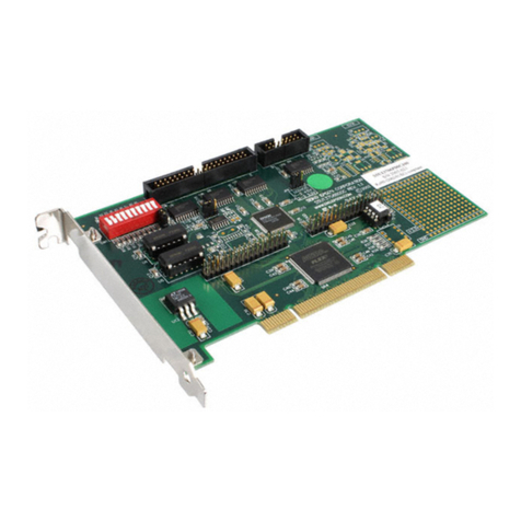
Texas Instruments TPS5420EVM-175 SWIFT User manual
Other Texas Instruments Motherboard manuals
Texas Instruments
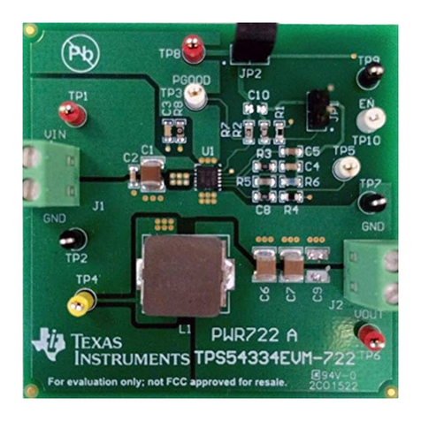
Texas Instruments TPS54334EVM-722 User manual
Texas Instruments
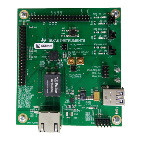
Texas Instruments DP838367 RGMII EVM User manual
Texas Instruments
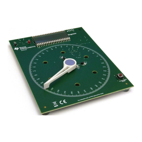
Texas Instruments DRV5055-ANGLE-EVM Series User manual
Texas Instruments
Texas Instruments TMP112EVM User manual
Texas Instruments
Texas Instruments TPS65400 User manual
Texas Instruments
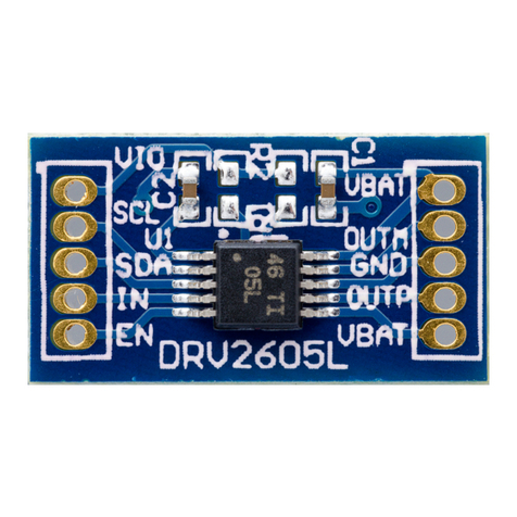
Texas Instruments DRV2605LDGSEVM-M User manual
Texas Instruments
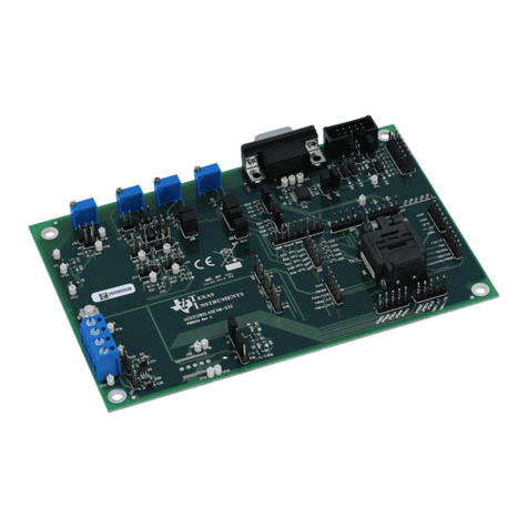
Texas Instruments UCD3138OL40EVM-032 User manual
Texas Instruments
Texas Instruments CC400DK User manual
Texas Instruments
Texas Instruments TPSI2140-Q1 User manual
Texas Instruments
Texas Instruments DS90UB95 Q1 Series User manual
Texas Instruments
Texas Instruments DEM-PCM2912A EVM User manual
Texas Instruments
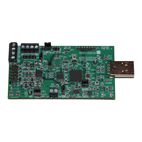
Texas Instruments ADS1x20EVM User manual
Texas Instruments
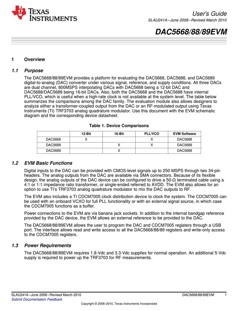
Texas Instruments DAC5668 User manual
Texas Instruments
Texas Instruments TPS25846-Q1 User manual
Texas Instruments
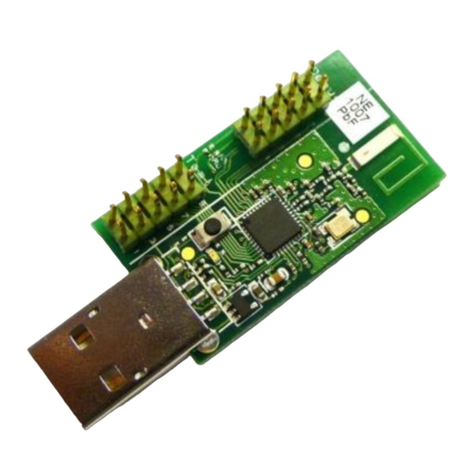
Texas Instruments CC1111 User manual
Texas Instruments
Texas Instruments TMS320DM6467 DVEVM User manual
Texas Instruments
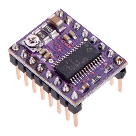
Texas Instruments DRV88 Series User manual
Texas Instruments
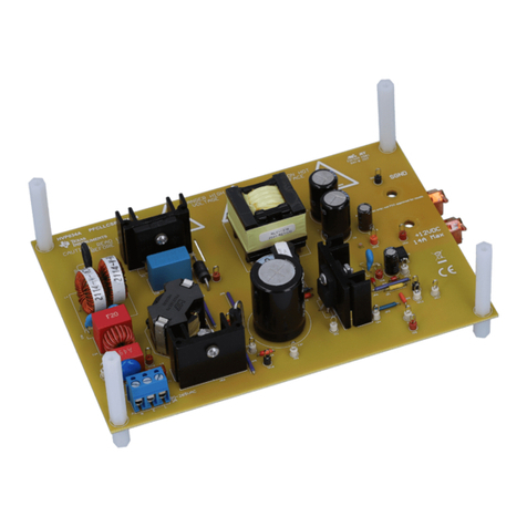
Texas Instruments PFCLLCSREVM034 User manual

Texas Instruments
Texas Instruments BQ24150 User manual
Texas Instruments
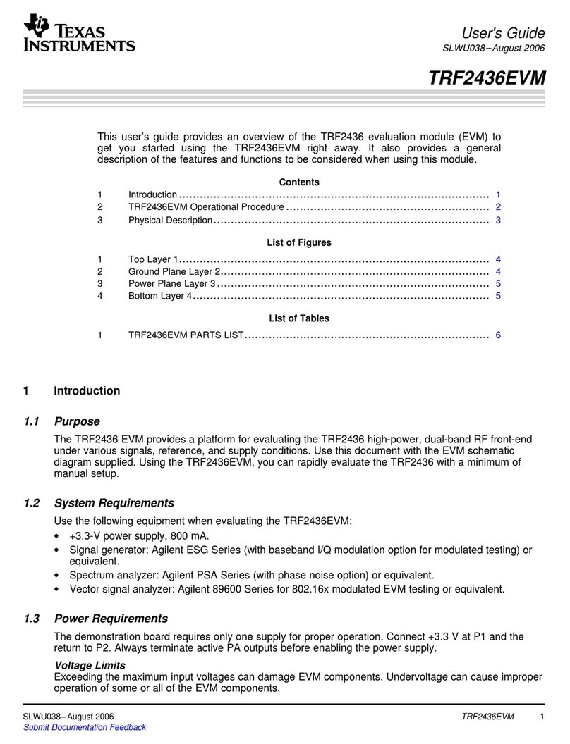
Texas Instruments Chipset TRF2436EVM User manual
