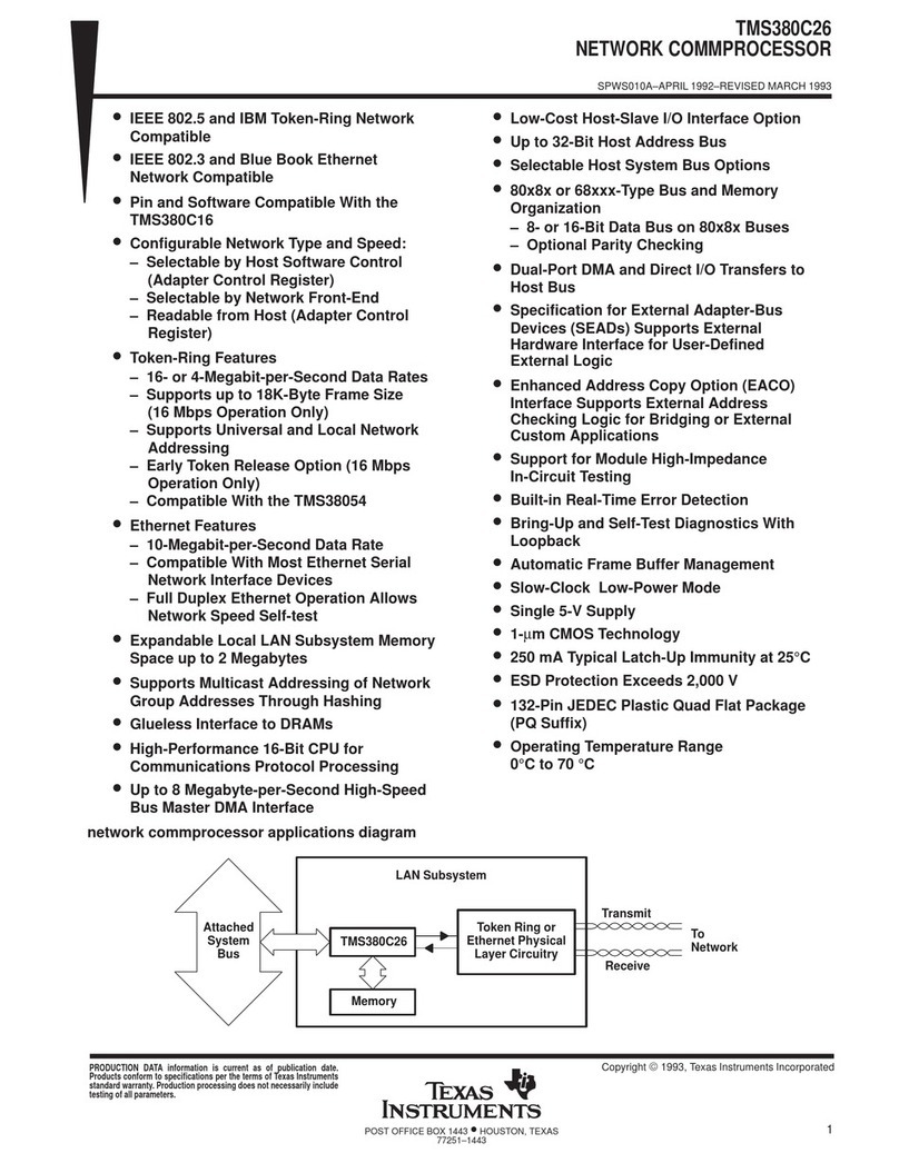
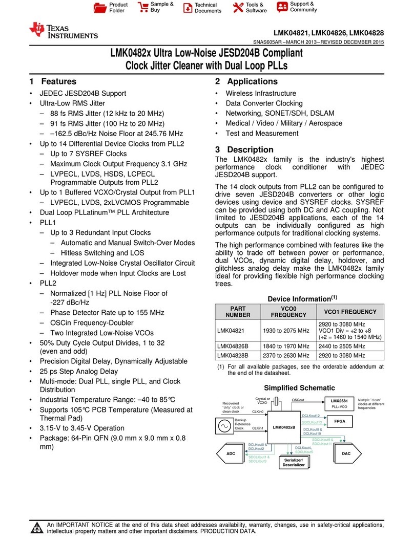
Texas Instruments LMK05318B EVM User manual

TI Confidential – NDA Restrictions
ADVANCE INFORMATION
APLL2
APLL1
I2C/SPI
LOGIC I/Os
STATUS
DPLL
÷R
XO/
TCXO/
OCXO
VDD
3.3 V
VDDO
1.8 / 2.5 / 3.3 V
Registers EEPROM,
ROM
Device Control
and Status
Power Conditioning
LMK05318
Ultra-Low Jitter
Network Synchronizer Clock
Hitless
Switching
Differential
or LVCMOS
Differential
or HCSL
DCO
PRIREF
SECREF VCO1
VCO2
OUT0
OUT1
OUT5
÷OD
OUT4÷OD
OUT2
OUT3
OUT7÷OD
OUT6
÷OD
×1, ×2
÷
÷
÷
Output
Muxes
Differential,
HCSL, or
1.8-V LVCMOS
÷
÷OD
÷OD
Product
Folder
Order
Now
Technical
Documents
Tools &
Software
Support &
Community
An IMPORTANT NOTICE at the end of this data sheet addresses availability, warranty, changes, use in safety-critical applications,
intellectual property matters and other important disclaimers. ADVANCE INFORMATION for pre-production products; subject to
change without notice.
LMK05318B
SNAS801 –OCTOBER 2019
LMK05318B Ultra-Low Jitter Network Synchronizer Clock With Two Frequency Domains
1
1 Features
1• One Digital Phase-Locked Loop (DPLL) With:
– Hitless Switching: ±50-ps Phase Transient
– Programmable Loop Bandwidth With Fastlock
– Standards-Compliant Synchronization and
Holdover Using a Low-Cost TCXO/OCXO
• Two Analog Phase-Locked Loops (APLLs) With
Industry-Leading Jitter Performance:
– 50-fs RMS Jitter at 312.5 MHz (APLL1)
– 125-fs RMS Jitter at 155.52 MHz (APLL2)
• Two Reference Clock Inputs
– Priority-Based Input Selection
– Digital Holdover on Loss of Reference
• Eight Clock Outputs With Programmable Drivers
– Up to Six Different Output Frequencies
– AC-LVDS, AC-CML, AC-LVPECL, HCSL, and
1.8-V LVCMOS Output Formats
• EEPROM / ROM for Custom Clocks on Power-Up
• Flexible Configuration Options
– 1 Hz (1 PPS) to 800 MHz on Input and Output
– XO/TCXO/OCXO Input: 10 to 100 MHz
– DCO Mode: < 0.001 ppb/Step for Precise
Clock Steering (IEEE 1588 PTP Slave)
– Advanced Clock Monitoring and Status
– I2C or SPI Interface
• PSNR: –83 dBc (50-mVpp Noise on 3.3-V Supply)
• 3.3-V Supply With 1.8-V, 2.5-V, or 3.3-V Outputs
• Industrial Temperature Range: –40°C to +85°C
2 Applications
• SyncE (G.8262), SONET/SDH (Stratum 3/3E,
G.813, GR-1244, GR-253), IEEE 1588 PTP Slave
Clock, or Optical Transport Network (G.709)
• 400G Line Cards, Fabric Cards for Ethernet
Switches and Routers
• Wireless Base Station (BTS), Wireless Backhaul
• Test and Measurement, Medical Imaging
• Jitter Cleaning, Wander Attenuation, and
Reference Clock Generation for 56G/112G PAM-4
PHYs, ASICs, FPGAs, SoCs, and Processors
3 Description
The LMK05318B is a high-performance network
synchronizer clock device that provides jitter cleaning,
clock generation, advanced clock monitoring, and
superior hitless switching performance to meet the
stringent timing requirements of communications
infrastructure and industrial applications. The ultra-
low jitter and high power supply noise rejection
(PSNR) of the device can reduce bit error rates
(BER) in high-speed serial links.
The device can generate output clocks with 50-fs
RMS jitter using TI's proprietary Bulk Acoustic Wave
(BAW) VCO technology, independent of the jitter and
frequency of the XO and reference inputs.
Device Information(1)
PART NUMBER PACKAGE BODY SIZE (NOM)
LMK05318B VQFN (48) 7.00 mm × 7.00 mm
(1) For all available packages, see the orderable addendum at
the end of the data sheet.
Simplified Block Diagram
TI Confidential – NDA Restrictions
ADVANCE INFORMATION
2
LMK05318B
SNAS801 –OCTOBER 2019
www.ti.com
Product Folder Links: LMK05318B
Submit Documentation Feedback Copyright © 2019, Texas Instruments Incorporated
Table of Contents
1 Features.................................................................. 1
2 Applications ........................................................... 1
3 Description............................................................. 1
4 Revision History..................................................... 2
5 Description (continued)......................................... 3
6 Pin Configuration and Functions......................... 4
6.1 Device Start-Up Modes............................................. 7
7 Specifications......................................................... 8
7.1 Absolute Maximum Ratings ...................................... 8
7.2 ESD Ratings.............................................................. 8
7.3 Recommended Operating Conditions....................... 8
7.4 Thermal Information: 4-Layer JEDEC Standard
PCB............................................................................ 9
7.5 Thermal Information: 10-Layer Custom PCB............ 9
7.6 Electrical Characteristics........................................... 9
7.7 Timing Diagrams..................................................... 15
7.8 Typical Characteristics............................................ 17
8 Parameter Measurement Information ................ 19
8.1 Output Clock Test Configurations........................... 19
9 Detailed Description............................................ 21
9.1 Overview................................................................. 21
9.2 Functional Block Diagram....................................... 22
9.3 Feature Description................................................. 26
9.4 Device Functional Modes........................................ 51
9.5 Programming .......................................................... 57
10 Application and Implementation........................ 64
10.1 Application Information.......................................... 64
10.2 Typical Application................................................ 68
10.3 Do's and Don'ts..................................................... 73
11 Power Supply Recommendations ..................... 74
11.1 Power Supply Bypassing ...................................... 74
11.2 Device Current and Power Consumption.............. 75
12 Layout................................................................... 76
12.1 Layout Guidelines ................................................. 76
12.2 Layout Example .................................................... 76
12.3 Thermal Reliability................................................. 77
13 Device and Documentation Support................. 78
13.1 Device Support...................................................... 78
13.2 Receiving Notification of Documentation Updates 78
13.3 Support Resources ............................................... 78
13.4 Trademarks........................................................... 78
13.5 Electrostatic Discharge Caution............................ 78
13.6 Glossary................................................................ 78
14 Mechanical, Packaging, and Orderable
Information........................................................... 78
4 Revision History
DATE REVISION NOTES
October 2018 * Initial release.

TI Confidential – NDA Restrictions
ADVANCE INFORMATION
3
LMK05318B
www.ti.com
SNAS801 –OCTOBER 2019
Product Folder Links: LMK05318B
Submit Documentation FeedbackCopyright © 2019, Texas Instruments Incorporated
5 Description (continued)
The DPLL supports programmable loop bandwidth for jitter and wander attenuation, while the two APLLs support
fractional frequency translation for flexible clock generation. The synchronization options supported on the DPLL
include hitless switching with phase cancellation, digital holdover, and DCO mode with less than 0.001-ppb (part
per billion) frequency step size for precision clock steering (IEEE 1588 PTP slave). The DPLL can phase-lock to
a 1-PPS (pulse-per-second) reference input and support optional zero-delay mode on one output to achieve
deterministic input-to-output phase alignment with programmable offset. The advanced reference input
monitoring block ensures robust clock fault detection and helps to minimize output clock disturbance when a loss
of reference (LOR) occurs.
The device can use a commonly available low-frequency TCXO or OCXO to set the free-run or holdover output
frequency stability per synchronization standards. Otherwise, the device can use a standard XO when free-run or
holdover frequency stability and wander are not critical. The device is fully programmable through I2C or SPI
interface and supports custom frequency configuration on power up with the internal EEPROM or ROM. The
EEPROM is factory pre-programmed and can be programmed in-system if needed.
See Typical Characteristics for Test Conditions.
Figure 1. 312.5-MHz Output Phase Noise (APLL1), < 50-fs RMS Jitter

TI Confidential – NDA Restrictions
ADVANCE INFORMATION
48 OUT7_P13PDN
1STATUS0 36 VDD_PLL2
47 OUT7_N14OUT0_P
2STATUS1/ FDEC 35 CAP_PLL2
46 VDDO_715OUT0_N
3CAP_DIG 34 LF2
45 OUT6_P16OUT1_N
4VDD_DIG 33 VDD_XO
44 OUT6_N17OUT1_P
5VDD_IN 32 XO_N
43 VDDO_618VDDO_01
6PRIREF_P 31 XO_P
42 OUT5_P19VDDO_23
7PRIREF_N 30 GPIO2/SDO/ FINC
41 OUT5_N20OUT2_P
8REFSEL 29 LF1
40 VDDO_521OUT2_N
9HW_SW_CTRL 28 CAP_PLL1
39 OUT4_P22OUT3_N
10SECREF_P 27 VDD_PLL1
38 OUT4_N23OUT3_P
11SECREF_N 26 SCL/SCK
37 VDDO_424GPIO1/SCS
12GPIO0/SYNCN 25 SDA/SDI
Not to scale
GND
4
LMK05318B
SNAS801 –OCTOBER 2019
www.ti.com
Product Folder Links: LMK05318B
Submit Documentation Feedback Copyright © 2019, Texas Instruments Incorporated
(1) G = Ground, P = Power, I = Input, O = Output, I/O = Input or Output, A = Analog.
6 Pin Configuration and Functions
RGZ Package
48-Pin QFN
Top View
Pin Functions
PIN TYPE(1) DESCRIPTION
NAME NO.
POWER
GND PAD G Ground / Thermal Pad.
The exposed pad must be connected to PCB ground for proper electrical and thermal performance.
A 5×5 via pattern is recommended to connect the IC ground pad to the PCB ground layers.
VDD_IN 5 P Core Supply (3.3 V) for Primary and Secondary Reference Inputs.
Place a nearby 0.1-µF bypass capacitor on each pin.
VDD_XO 33 P Core Supply (3.3 V) for XO Input.
Place a nearby 0.1-µF bypass capacitor on each pin.
VDD_PLL1 27 P Core Supply (3.3 V) for PLL1, PLL2, and Digital Blocks.
Place a nearby 0.1-µF bypass capacitor on each pin.
VDD_PLL2 36 P
VDD_DIG 4 P

TI Confidential – NDA Restrictions
ADVANCE INFORMATION
5
LMK05318B
www.ti.com
SNAS801 –OCTOBER 2019
Product Folder Links: LMK05318B
Submit Documentation FeedbackCopyright © 2019, Texas Instruments Incorporated
Pin Functions (continued)
PIN TYPE(1) DESCRIPTION
NAME NO.
VDDO_01 18 P
Output Supply (1.8, 2.5, or 3.3 V) for Clock Outputs 0 to 7.
Place a nearby 0.1-µF bypass capacitor on each pin.
VDDO_23 19 P
VDDO_4 37 P
VDDO_5 40 P
VDDO_6 43 P
VDDO_7 46 P
CORE BLOCKS
LF1 29 A External Loop Filter Capacitor for APLL1 and APLL2.
Place a nearby capacitor on each pin. For LF1, 0.47-µF is suggested for typical APLL1 loop
bandwidths around 2.5 kHz. For LF2, 0.1-µF is suggested for typical APLL2 loop bandwidth around
500 kHz.
LF2 34 A
CAP_PLL1 28 A External Bypass Capacitors for APLL1, APLL2, and Digital Blocks.
Place a nearby 10-µF bypass capacitor on each pin.
CAP_PLL2 35 A
CAP_DIG 3 A
INPUT BLOCKS
PRIREF_P 6 I DPLL Primary and Secondary Reference Clock Inputs.
Each input pair can accept a differential or single-ended clock as a reference to the DPLL. Each
pair has a programmable input type with internal termination to support AC- or DC-coupled clocks.
A single-ended LVCMOS clock can be applied to the P input with the N input pulled down to
ground. An unused input pair can be left floating.
PRIREF_N 7 I
SECREF_P 10 I
SECREF_N 11 I
XO_P 31 I XO/TCXO/OCXO Input.
This input pair can accept a differential or single-ended clock signal from a low-jitter local oscillator
as a reference to the APLLs. This input has a programmable input type with internal termination to
support AC- or DC-coupled clocks. A single-ended LVCMOS clock (up to 2.5 V) can be applied to
the P input with the N input pulled down to ground. A low-frequency TCXO or OCXO can be used to
set the clock output frequency accuracy and stability during free-run and holdover modes.
In DPLL mode, the XO frequency must have a non-integer relationship to the VCO1 frequency so
APLL1 can operate in fractional mode (required for proper DPLL operation). In APLL-only mode, the
XO frequency can have either an integer or non-integer relationship to the VCO1 frequency.
XO_N 32 I
OUTPUT BLOCKS
OUT0_P 14 O
Clock Outputs 0 to 3 Bank.
Each programmable output driver pair can support AC-LVDS, AC-CML, AC-LVPECL and HCSL.
Unused differential outputs should be terminated if active or left floating if disabled through registers.
The OUT[0:3] bank is preferred for PLL1 clocks to minimize output crosstalk.
OUT0_N 15 O
OUT1_P 17 O
OUT1_N 16 O
OUT2_P 20 O
OUT2_N 21 O
OUT3_P 23 O
OUT3_N 22 O
OUT4_P 39 O
Clock Outputs 4 to 7 Bank.
Each programmable output driver pair can support AC-LVDS, AC-CML, AC-LVPECL, HCSL, or 1.8-
V LVCMOS clocks (one or two per pair). Unused differential outputs should be terminated if active
or left floating if disabled through registers.
The OUT[4:7] bank is preferred for PLL2 clocks to minimize output crosstalk. When PLL2 is not
used, the OUT[4:7] bank can be used for PLL1 clocks without risk of cross-coupling from PLL2.
OUT4_N 38 O
OUT5_P 42 O
OUT5_N 41 O
OUT6_P 45 O
OUT6_N 44 O
OUT7_P 48 O
OUT7_N 47 O

TI Confidential – NDA Restrictions
ADVANCE INFORMATION
6
LMK05318B
SNAS801 –OCTOBER 2019
www.ti.com
Product Folder Links: LMK05318B
Submit Documentation Feedback Copyright © 2019, Texas Instruments Incorporated
Pin Functions (continued)
PIN TYPE(1) DESCRIPTION
NAME NO.
(2) Internal resistors: PDN pin has 200-kΩpullup to VDD_IN. HW_SW_CTRL, GPIO, REFSEL, and STATUS pins each have a 150-kΩbias
to VIM (approximately 0.8 V) when PDN = 0 or 400-kΩpulldown when PDN = 1.
(3) Unless otherwise noted: Logic inputs are 2-level, 1.8-V compatible inputs. Logic outputs are 3.3-V LVCMOS levels.
LOGIC CONTROL / STATUS (2)(3)
HW_SW_CTRL 9 I
Device Start-Up Mode Select (3-level, 1.8-V compatible).
This input selects the device start-up mode that determines the memory page used to initialize the
registers, serial interface, and logic pin functions. The input level is sampled only at device power-
on reset (POR).
See Table 1 for start-up mode descriptions and logic pin functions.
PDN 13 I
Device Power-Down (active low).
When PDN is pulled low, the device is in hard-reset and all blocks including the serial interface are
powered down. When PDN is pulled high, the device is started according to device mode selected
by HW_SW_CTRL and begins normal operation with all internal circuits reset to their initial state.
SDA/SDI 25 I/O
I2C Serial Data I/O (SDA) or SPI Serial Data Input (SDI). See Table 1.
When HW_SW_CTRL is 0 or 1, the serial interface is I2C. SDA and SCL pins (open drain) require
external I2C pullup resistors. The default 7-bit I2C address is 11001xxb, where the MSB bits
(11001b) are initialized from on-chip EEPROM and the LSB bits (xxb) are determined by the logic
input pins. When HW_SW_CTRL is 0, the LSBs are determined by the GPIO1 input state (3-level)
during POR. When HW_SW_CTRL is 1, the LSBs are fixed to 00b.
When HW_SW_CTRL is Float, the serial interface is SPI (4-wire, Mode 0) using the SDI, SCK,
SCS, and SDO pins.
SCL/SCK 26 I I2C Serial Clock Input (SCL) or SPI Serial Clock Input (SCK). See Table 1.
GPIO0/SYNCN 12 I
Multifunction Inputs or Outputs.
See Table 1.
GPIO1/SCS 24 I
GPIO2/SDO/
FINC 30 I/O
STATUS0 1 I/O Status Outputs 0 and 1.
Each output has programmable status signal selection, driver type (3.3-V LVCMOS or open-drain),
and status polarity. Open-drain requires an external pullup resistor. Leave pin floating if unused.
In I2C mode, the STATUS1/FDEC pin can function as a DCO mode control input pin. See Table 1.
STATUS1/
FDEC 2 I/O
REFSEL 8 I Manual DPLL Reference Clock Input Selection. (3-level, 1.8-V compatible).
REFSEL = 0 (PRIREF), 1 (SECREF), or Float or VIM (Auto Select). This control pin must be
enabled by register default or programming. Leave pin floating if unused.

TI Confidential – NDA Restrictions
ADVANCE INFORMATION
7
LMK05318B
www.ti.com
SNAS801 –OCTOBER 2019
Product Folder Links: LMK05318B
Submit Documentation FeedbackCopyright © 2019, Texas Instruments Incorporated
(1) The input levels on these pins are sampled only during POR.
(2) FINC and FDEC pins are only available when DCO mode and GPIO pin control are enabled by registers.
6.1 Device Start-Up Modes
The HW_SW_CTRL input pin selects the device start-up mode that determines the memory page (EEPROM or
ROM) used to initialize the registers, the serial interface, and the logic pin functions at power-on reset. The initial
register settings determine the device's frequency configuration on start-up. After start-up, the device registers
can be accessed through the serial interface for device monitoring and programming, and the logic pins will
function as defined by the selected mode.
Table 1. Device Start-Up Modes
HW_SW_CTRL
INPUT LEVEL(1) START-UP
MODE MODE DESCRIPTION
0EEPROM + I2C
(Soft pin mode)
Registers are initialized from EEPROM, and I2C interface is enabled.
Logic pins:
•SDA/SDI, SCL/SCK: I2C Data, I2C Clock (open drain)
•GPIO0/SYNCN: Output SYNC Input (active low). Pull up externally if not used.
•GPIO1/SCS(1): I2C Address LSB Select (Low = 00b, Float = 01b, High = 10b)
•GPIO2/SDO/FINC(2): DPLL DCO Frequency Increment (active high)
•STATUS1/FDEC(2): DPLL DCO Frequency Decrement (active high), or Status output
Float
(VIM)EEPROM + SPI
(Soft pin mode)
Registers are initialized from EEPROM, and SPI interface is enabled.
Logic pins:
•SDA/SDI, SCL/SCK: SPI Data In (SDI), SPI Clock (SCK)
•GPIO0/SYNCN: Output SYNC Input (active low). Pull up externally if not used.
•GPIO1/SCS: SPI Chip Select (SCS)
•GPIO2/SDO/FINC: SPI Data Out (SDO)
1ROM + I2C
(Hard pin mode)
Registers are initialized from the ROM page selected by GPIO pins, and I2C interface is enabled.
Logic pins:
•SDA/SDI, SCL/SCK: I2C Data, I2C Clock (open drain)
•GPIO[2:0] (1): ROM Page Select Inputs (000b to 111b) during POR.
• After POR, GPIO2/SDO/FINC and STATUS1/FDEC pins can function the same as for
HW_SW_CTRL = 0.
NOTE
To ensure proper start-up into EEPROM + SPI Mode, the HW_SW_CTRL, STATUS0, and
STATUS1 pins must all be floating or biased to VIM (0.8-V typical) before the PDN pin is
pulled high. These three pins momentarily operate as 3-level inputs and get sampled at
the low-to-high transition of PDN to determine the device start-up mode during POR. If
any of these pins are connected to a system host (MCU or FPGA), TI recommends using
external biasing resistors on each pin (10-kΩpullup to 3.3 V with 3.3-kΩpulldown to GND)
to set the inputs to VIM during POR. After power-up, the STATUS pins can operate as
LVCMOS outputs to overdrive the external resistor bias for normal status operation.

TI Confidential – NDA Restrictions
ADVANCE INFORMATION
8
LMK05318B
SNAS801 –OCTOBER 2019
www.ti.com
Product Folder Links: LMK05318B
Submit Documentation Feedback Copyright © 2019, Texas Instruments Incorporated
(1) Stresses beyond those listed under Absolute Maximum Ratings may cause permanent damage to the device. These are stress ratings
only, which do not imply functional operation of the device at these or any other conditions beyond those indicated under Recommended
Operating Conditions. Exposure to absolute-maximum-rated conditions for extended periods may affect device reliability.
(2) VDD refers to all core supply pins or voltages. All VDD core supplies should be powered-on before the PDN is pulled high to trigger the
internal power-on reset (POR).
(3) VDDO refers to all output supply pins or voltages. VDDO_x refers to the output supply for a specific output channel, where x denotes
the channel index.
7 Specifications
7.1 Absolute Maximum Ratings
Over operating free-air temperature range (unless otherwise noted)(1)
MIN MAX UNIT
VDD(2) Core supply voltages -0.3 3.6 V
VDDO(3) Output supply voltages -0.3 3.6 V
VIN Input voltage range for clock and logic inputs -0.3 VDD+0.3 V
VOUT_LOGIC Output voltage range for logic outputs -0.3 VDD+0.3 V
VOUT Output voltage range for clock outputs -0.3 VDDO+0.3 V
TJJunction temperature 150 °C
Tstg Storage temperture range -65 150 °C
(1) JEDEC document JEP155 states that 500-V HBM allows safe manufacturing with a standard ESD control process.
(2) JEDEC document JEP157 states that 250-V CDM allows safe manufacturing with a standard ESD control process.
7.2 ESD Ratings VALUE UNIT
V(ESD) Electrostatic
discharge
Human body model (HBM), per ANSI/ESDA/JEDEC JS-001, all pins(1) ±2000 V
Charged device model (CDM), per JEDEC specification JESD22-C101, all
pins(2) ±750
(1) VDD refers to all core supply pins or voltages. All VDD core supplies should be powered-on before internal power-on reset (POR).
(2) VDDO refers to all output supply pins or voltages. VDDO_x refers to the output supply for a specific output channel, where x denotes
the channel index.
(3) The LVCMOS driver supports full rail-to-rail swing when VDDO_x is 1.8 V ±5%. When VDDO_x is 2.5 V or 3.3 V, the LVCMOS driver
will not fully swing to the positive rail due to the dropout voltage of the output channel's internal LDO regulator.
(4) Time for VDD to ramp monotonically above 2.7 V for proper internal power-on reset. For slower or non-monotonic VDD ramp, hold PDN
low until after VDD voltages are valid.
(5) nEEcyc specifies the maximum EEPROM program cycles allowed for customer programming. The initial count of factory-programmed
cycles is non-zero due to production tests, but factory-programmed cycles are excluded from the nEEcyc limit. The total number of
EEPROM program cycles can be read from the 8-bit NVM count status register (NVMCNT), which automatically increments by 1 on
each successful programming cycle. TI does not ensure EEPROM endurance if the nEEcyc limit is exceeded by the customer.
7.3 Recommended Operating Conditions
Over operating free-air temperature range (unless otherwise noted) MIN NOM MAX UNIT
VDD(1) Core supply voltages 3.135 3.3 3.465 V
VDDO_x(2) Output supply voltage for AC-LVDS/CML/LVPECL or HCSL driver 1.71 1.8, 2.5, 3.3 3.465 V
VDDO_x(2) Output supply voltage for 1.8-V LVCMOS driver(3) 1.71 1.8 1.89 V
VIN Input voltage range for clock and logic inputs 0 3.465 V
TJJunction temperature 135 °C
tVDD Power supply ramp time(4) 0.01 100 ms
nEEcyc EEPROM program cycles(5) 100 cycles

TI Confidential – NDA Restrictions
ADVANCE INFORMATION
9
LMK05318B
www.ti.com
SNAS801 –OCTOBER 2019
Product Folder Links: LMK05318B
Submit Documentation FeedbackCopyright © 2019, Texas Instruments Incorporated
(1) For more information about traditional and new thermal metrics, see the Semiconductor and IC Package Thermal Metrics application
report, SPRA953.
(2) The thermal information is based on a 4-layer JEDEC standard board with 25 thermal vias (5 x 5 pattern, 0.3 mm holes).
(3) ΨJB can allow the system designer to measure the board temperature (TPCB) with a fine-gauge thermocouple and back-calculate the
device junction temperature, TJ= TPCB + (ΨJB x Power). Measurement of ΨJB is defined by JESD51-6.
7.4 Thermal Information: 4-Layer JEDEC Standard PCB
THERMAL METRIC(1)(2)(3)
LMK05318B
UNITRGZ (VQFN)
48 PINS
RθJA Junction-to-ambient thermal resistance 23.3 °C/W
RθJC(top) Junction-to-case (top) thermal resistance 13.2 °C/W
RθJB Junction-to-board thermal resistance 7.4 °C/W
RθJC(bot) Junction-to-case (bottom) thermal resistance 1.4 °C/W
ψJT Junction-to-top characterization parameter 0.2 °C/W
ψJB Junction-to-board characterization parameter 7.3 °C/W
(1) For more information about traditional and new thermal metrics, see the Semiconductor and IC Package Thermal Metrics application
report, SPRA953.
(2) The thermal information is based on a 10-layer 200 mm x 250 mm x 1.6 mm board with 25 thermal vias (5 x 5 pattern, 0.3 mm holes).
(3) ΨJB can allow the system designer to measure the board temperature (TPCB) with a fine-gauge thermocouple and back-calculate the
device junction temperature, TJ= TPCB + (ΨJB x Power). Measurement of ΨJB is defined by JESD51-6.
7.5 Thermal Information: 10-Layer Custom PCB
THERMAL METRIC(1) (2) (3)
LMK05318B
UNITRGZ (VQFN)
48 PINS
RθJA Junction-to-ambient thermal resistance 9.1 °C/W
RθJB Junction-to-board thermal resistance 4.4 °C/W
ψJT Junction-to-top characterization parameter 0.2 °C/W
ψJB Junction-to-board characterization parameter 4.4 °C/W
7.6 Electrical Characteristics
Over Recommended Operating Conditions (unless otherwise noted)
PARAMETER TEST CONDITIONS MIN TYP MAX UNIT
POWER SUPPLY CHARACTERISTICS
IDD_DIG Core Current Consumption
(VDD_DIG) 18 mA
IDD_IN Core Current Consumption
(VDD_IN) 38 mA
IDD_PLL1 Core Current Consumption
(VDD_PLL1) DPLL and APLL1 enabled 110 mA
IDD_XO Core Current Consumption
(VDD_XO) 20 mA
IDD_PLL2 Core Current Consumption
(VDD_PLL2) APLL2 disabled 20 mA
APLL2 enabled 120 mA

TI Confidential – NDA Restrictions
ADVANCE INFORMATION
10
LMK05318B
SNAS801 –OCTOBER 2019
www.ti.com
Product Folder Links: LMK05318B
Submit Documentation Feedback Copyright © 2019, Texas Instruments Incorporated
Electrical Characteristics (continued)
Over Recommended Operating Conditions (unless otherwise noted)
PARAMETER TEST CONDITIONS MIN TYP MAX UNIT
(1) IDDO_x current for an operating output is the sum of mux, divider and an output format.
(2) Minimum limit applies for the minimum setting of the differential input amplitude monitor (xREF_LVL_SEL = 0).
(3) In order to meet the jitter performance listed in the subsequent sections of this data sheet, the minimum recommended slew rate for all
input clocks is 0.5 V/ns. This is especially true for single-ended clocks. Phase noise performance will begin to degrade as the clock
input slew rate is reduced. However, the device will function at slew rates down to the minimum listed. When compared to single-
ended clocks, differential clocks (LVDS, LVPECL) will be less susceptible to degradation in phase noise performance at lower slew rates
due to their common mode noise rejection. However, it is also recommended to use the highest possible slew rate for differential clocks
to achieve optimal phase noise performance at the device outputs.
(4) For a differential input clock below 5 MHz, TI recommends to disable the differential input amplitude monitor and enable at least one
other monitor (frequency, window detectors) to validate the input clock. Otherwise, consider using an LVCMOS clock for an input below
5 MHz.
IDDO_x Output Current Consumption, per
channel(1)
(VDDO_x)
Output mux and divider enabled,
excludes driver(s)
Divider value = 2 to 6 50 mA
Output mux and divider enabled,
excludes driver(s)
Divider value > 6 70 mA
AC-LVDS 11 mA
AC-CML 14 mA
AC-LVPECL 16 mA
HCSL, 50-Ωload to GND 25 mA
1.8-V LVCMOS (x2), 100 MHz 6 mA
IDDPDN Total Current Consumption (all
VDD and VDDO pins, 3.3 V) Device powered-down (PDN pin held
low) 56 mA
XO INPUT CHARACTERISTICS (XO)
fIN Input frequency range 10 100 MHz
VIN-SE Single-ended input voltage swing LVCMOS input, DC-coupled to XO_P 1 2.6 Vpp
VIN-DIFF Differential input voltage swing(2) Differential input 0.4 2 Vpp
VID Differential input voltage swing(2) Differential input 0.2 1 |V|
dV/dt Input slew rate(3) 0.2 0.5 V/ns
IDC Input duty cycle 40 60 %
IIN Input leakage 50-Ωand 100-Ωinternal terminations
disabled -350 350 µA
REFERENCE INPUT CHARACTERISTICS (PRIREF, SECREF)
fIN Input frequency range Differential input(4) 5 800 MHz
fIN Input frequency range LVCMOS input 1E-6 250 MHz
VIH Input high voltage LVCMOS input, DC-coupled to REF_P.
Internally DC coupled 1.2 V
VIL Input low voltage LVCMOS input, DC-coupled to REF_P.
Internally DC coupled 0.6 V
VIN-SE Single-ended input voltage swing LVCMOS input, DC-coupled to REF_P.
Internally AC coupled 1 2.6 Vpp
VIN-DIFF Differential input voltage swing(2) Differential input 0.4 2 Vpp
VID Differential input voltage swing(2) Differential input 0.2 1 V
VCM Differential Input Common Mode Differential Input, DC-coupled to REF tbd tbd V
dV/dt Input slew rate(3) 0.2 0.5 V/ns
IIN Input leakage 50-Ωand 100-Ωinternal terminations
disabled -350 350 µA
VCO CHARACTERISTICS
fVCO1 VCO1 Frequency Range 2499.750 2500 2500.250 MHz
fVCO2 VCO2 Frequency Range 5500 6250 MHz

TI Confidential – NDA Restrictions
ADVANCE INFORMATION
11
LMK05318B
www.ti.com
SNAS801 –OCTOBER 2019
Product Folder Links: LMK05318B
Submit Documentation FeedbackCopyright © 2019, Texas Instruments Incorporated
Electrical Characteristics (continued)
Over Recommended Operating Conditions (unless otherwise noted)
PARAMETER TEST CONDITIONS MIN TYP MAX UNIT
(5) An output frequency over fOUT max spec is possible, but output swing may be less than VOD min specification.
(6) Measured on the differential output waveform (OUTx_P - OUTx_N).
(7) Parameter is specified for PLL outputs divided from either VCO domain.
APLL CHARACTERISTICS
fPD1 APLL1 Phase Detector
Frequency 1 50 MHz
fPD2 APLL2 Phase Detector
Frequency 10 150 MHz
AC-LVDS OUTPUT CHARACTERISTICS (OUTx)
fOUT Output frequency(5) 800 MHz
VOD Output voltage swing (VOH - VOL) fOUT ≥25 MHz; TYP at 156.25 MHz 250 350 450 mV
VOUT-DIFF Differential output voltage swing,
peak-to-peak 2×VOD Vpp
VOS Output common mode 100 430 mV
tSK Output-to-output skew Same post divider, output divide
values, and output type 100 ps
tR/tFOutput rise/fall time(6) 20% to 80%, < 300 MHz 225 350 ps
± 100 mV around center point, ≥300
MHz 85 250 ps
PNFLOOR Output phase noise floor fOUT = 156.25 MHz; fOFFSET > 10 MHz -160 dBc/Hz
ODC Output duty cycle(7) 45 55 %
AC-CML OUTPUT CHARACTERISTICS (OUTx)
fOUT Output frequency(5) 800 MHz
VOD Output voltage swing (VOH - VOL) TYP at fOUT = 156.25 MHz 400 600 800 mV
VOUT-DIFF Differential output voltage swing,
peak-to-peak 2×VOD Vpp
VOS Output common mode 150 550 mV
tSK Output-to-output skew Same post divider, output divide
values, and output type 100 ps
tR/tFOutput rise/fall time(6) 20% to 80%, < 300 MHz 225 300 ps
± 100 mV around center point, ≥300
MHz 50 150 ps
PNFLOOR Output phase noise floor fOUT = 156.25 MHz; fOFFSET > 10 MHz -160 dBc/Hz
ODC Output duty cycle(7) 45 55 %
AC-LVPECL OUTPUT CHARACTERISTICS (OUTx)
fOUT Output frequency(5) 800 MHz
VOD Output voltage swing (VOH - VOL) TYP at fOUT = 156.25 MHz 500 800 1000 mV
VOUT-DIFF Differential output voltage swing,
peak-to-peak 2×VOD Vpp
VOS Output common mode 300 700 mV
tSK Output-to-output skew Same post divider, output divide
values, and output type 100 ps
tR/tFOutput rise/fall time(6) 20% to 80%, < 300 MHz 200 300 ps
± 100 mV around center point, ≥300
MHz 35 100 ps
PNFLOOR Output phase noise floor fOUT = 156.25 MHz; fOFFSET > 10 MHz -162 dBc/Hz
ODC Output duty cycle(7) 45 55 %

TI Confidential – NDA Restrictions
ADVANCE INFORMATION
12
LMK05318B
SNAS801 –OCTOBER 2019
www.ti.com
Product Folder Links: LMK05318B
Submit Documentation Feedback Copyright © 2019, Texas Instruments Incorporated
Electrical Characteristics (continued)
Over Recommended Operating Conditions (unless otherwise noted)
PARAMETER TEST CONDITIONS MIN TYP MAX UNIT
HCSL OUTPUT CHARACTERISTICS (OUTx)
fOUT Output frequency(5) 400 MHz
VOH Output high voltage 600 880 mV
VOL Output low voltage -150 150 mV
tSK Output-to-output skew Same post divider, output divide
values, and output type 100 ps
dV/dt Output slew rate(6) ± 150 mV around center point 1 4 V/ns
PNFLOOR Output phase noise floor (fOFFSET
> 10 MHz) 100 MHz -160 dBc/Hz
ODC Output duty cycle(7) 45 55 %
1.8-V LVCMOS OUTPUT CHARACTERISTICS (OUT[4:7])
VOH Output high voltage IOH = 1 mA 1.2 V
VOL Output low voltage IOL = 1 mA 0.4 V
IOH Output high current -23 mA
IOL Output low current 20 mA
tR/tFOutput rise/fall time 20% to 80% 250 ps
tSK Output-to-output skew Same post divider, output divide
values, and output type 100 ps
tSK Output-to-output skew Same post divider, output divide
values, LVCMOS-to-DIFF 1.5 ns
PNFLOOR Output phase noise floor fOUT = 66.66 MHz; fOFFSET > 10 MHz -160 dBc/Hz
ODC Output duty cycle(7) 45 55 %
ROUT Output impedance 50 Ω
fOUT Output frequency 1E-6 200 MHz
3-LEVEL LOGIC INPUT CHARACTERISTICS (HW_SW_CTRL, GPIO1, REFSEL, STATUS[1:0])
VIH Input high voltage 1.4 V
VIM Input mid voltage Input floating with internal bias and
PDN pulled low 0.7 0.9 V
VIL Input low voltage 0.4 V
IIH Input high current VIH = VDD -40 40 µA
IIL Input low current VIL = GND -40 40 µA
2-LEVEL LOGIC INPUT CHARACTERISTICS (PDN, GPIO[2:0], SDI, SCK, SCS)
VIH Input high voltage 1.2 V
VIL Input low voltage 0.6 V
IIH Input high current VIH = VDD -40 40 µA
IIL Input low current VIL = GND -40 40 µA

TI Confidential – NDA Restrictions
ADVANCE INFORMATION
13
LMK05318B
www.ti.com
SNAS801 –OCTOBER 2019
Product Folder Links: LMK05318B
Submit Documentation FeedbackCopyright © 2019, Texas Instruments Incorporated
Electrical Characteristics (continued)
Over Recommended Operating Conditions (unless otherwise noted)
PARAMETER TEST CONDITIONS MIN TYP MAX UNIT
LOGIC OUTPUT CHARACTERISTICS (STATUS[1:0], SDO)
VOH Output high voltage IOH = 1 mA 1.2 V
VOL Output low voltage IOL = 1 mA 0.6 V
tR/tFOutput rise/fall time 20% to 80%, LVCMOS mode, 1 kΩto
GND 500 ps
SPI TIMING REQUIREMENTS (SDI, SCK, SCS, SDO)
fSCK SPI clock rate 20 MHz
SPI clock rate; NVM write 5 MHz
t1SCS to SCK setup time 10 ns
t2SDI to SCK setup time 10 ns
t3SDI to SCK hold time 10 ns
t4SCK high time 25 ns
t5SCK low time 25 ns
t6SCK to SDO valid read-back data 20 ns
t7SCS pulse width 20 ns
t8SDI to SCK hold time 10 ns
I2C-COMPATIBLE INTERFACE CHARACTERISTICS (SDA, SCL)
VIH Input high voltage 1.2 V
VIL Input low voltage 0.5 V
IIH Input leakage -15 15 µA
VOL Output low voltage IOL = 3 mA 0.3 V
fSCL I2C clock rate Standard 100 kHz
Fast mode 400
tSU(START) START condition setup time SCL high before SDA low 0.6 µs
tH(START) START condition hold time SCL low after SDA low 0.6 µs
tW(SCLH) SCL pulse width high 0.6 µs
tW(SCLL) SCL pulse width low 1.3 µs
tSU(SDA) SDA setup time 100 ns
tH(SDA) SDA hold time SDA valid after SCL low 0 0.9 µs
tR(IN) SDA/SCL input rise time 300 ns
tF(IN) SDA/SCL input fall time 300 ns
tF(OUT) SDA output fall time CBUS ≤400 pF 300 ns
tSU(STOP) STOP condition setup time 0.6 µs
tBUS Bus free time between STOP and
START 1.3 µs

TI Confidential – NDA Restrictions
ADVANCE INFORMATION
14
LMK05318B
SNAS801 –OCTOBER 2019
www.ti.com
Product Folder Links: LMK05318B
Submit Documentation Feedback Copyright © 2019, Texas Instruments Incorporated
Electrical Characteristics (continued)
Over Recommended Operating Conditions (unless otherwise noted)
PARAMETER TEST CONDITIONS MIN TYP MAX UNIT
(8) PSNR is the single-sideband spur level (in dBc) measured when sinusoidal noise with ampitude VNand frequency fN(between 100 kHz
and 1 MHz) is injected onto VDD and VDDO_x pins.
(9) DJSPUR (ps pk-pk) = [2 × 10(dBc/20) / (π× fOUT) × 1E6], where dBc is the PSNR or SPUR level (in dBc) and fOUT is the output frequency
(in MHz).
(10) Excluding output coupling spurs
(11) Actual loop bandwidth may be lower. The valid loop bandwidth range may be constrained by the DPLL TDC frequency used in a given
configuration.
(12) DPLL closed-loop jitter peaking of 0.1 dB or less is based on the DPLL bandwidth setting configured by the TICS Pro software tool.
POWER SUPPLY NOISE REJECTION (PSNR) / CROSSTALK SPURS
PSNR Spur induced by power supply
noise (VN= 50 mVpp) (8)(9)
VDD = 3.3 V, VDDO_x = 3.3 V, 156.25
MHz, AC-DIFF output –83 dBc
VDD = 3.3 V, VDDO_x = 3.3 V, 156.25
MHz, HCSL output –78 dBc
PSNR Spur induced by power supply
noise (VN= 25 mVpp)(8)(9)
VDD = 3.3 V, VDDO_x = 1.8 V, 156.25
MHz, AC-DIFF output –63 dBc
VDD = 3.3 V, VDDO_x = 1.8 V, 156.25
MHz, HCSL output –58 dBc
VDD = 3.3 V, VDDO_x = 1.8 V, 156.25
MHz, LVCMOS output –45 dBc
SPURXTALK Spur level due to output-to-output
crosstalk (adjacent channels)(9) fOUTx = 156.25 MHz, fOUTy = 155.52
MHz, AC-LVPECL –75 dBc
SPUR Highest spur level within 12 kHz
to 40 MHz band (excludes output
crosstalk and integer-boundary
spurs)(9)
fVCO1 = 2500 MHz, fVCO2 = 6065.28
MHz, fOUTx = 156.25 MHz, fOUTy =
155.52 MHz, AC-LVPECL –80 dBc
PLL CLOCK OUTPUT PERFORMANCE CHARACTERISTICS
RJ RMS Phase Jitter (12 kHz to 20
MHz), including spurs(10) 312.5 MHz AC-DIFF output from
APLL1, fXO = 48.0048 MHz, fPD1 =
fXO/2, fVCO1 = 2.5 GHz 50 100 fs RMS
RJ RMS Phase Jitter (12 kHz to 20
MHz), including spurs(10) 156.25 MHz AC-DIFF output from
APLL1, fXO = 48.0048 MHz, fPD1 =
fXO/2, fVCO1 = 2.5 GHz 60 100 fs RMS
RJ RMS Phase Jitter (12 kHz to 20
MHz), including spurs(10)
153.6 MHz AC-DIFF output from
APLL2, fXO = 48.0048 MHz, fPD1 =
fXO/2, fVCO1 = 2.5 GHz, fPD2 = fVCO1/18,
fVCO2 = 5.5296 GHz 125 250 fs RMS
RJ RMS Phase Jitter (12 kHz to 20
MHz), including spurs(10)
155.52 MHz AC-DIFF output from
APLL2, fXO = 48.0048 MHz, fPD1 =
fXO/2, fVCO1 = 2.5 GHz, fPD2 = fVCO1/18,
fVCO2 = 5.59872 GHz 125 250 fs RMS
BW DPLL bandwidth range(11) Programmed bandwidth setting 0.01 4000 Hz
JPK DPLL closed-loop jitter
peaking(12) fREF = 25 MHz, fOUT = 10 MHz, DPLL
BW = 0.1 Hz or 10 Hz 0.1 dB
JTOL Jitter tolerance Jitter modulation = 10 Hz, 25.78125
Gbps 6455 UI p-p
tHITLESS Phase hit between two reference
inputs with 0 ppm error Valid for a single switchover event
between two clock inputs at the same
frequency ± 50 ps
fHITLESS Frequency transient during hitless
switch Valid for a single switchover event
between two clock inputs at the same
frequency ± 10 ppb

TI Confidential – NDA Restrictions
ADVANCE INFORMATION
VOD = VOH - VOL
OUTx_N
OUTx_P
VOUT-DIFF = 2 × VOD
0 V
20%
80%
tRtF
VOH
VOL
STOP
~
~
START
STOP
~
~
~
~
~
~~
~
tBUS
tSU(START)
SDA
SCL
th(START) tr(SM)
tSU(SDATA)
tW(SCLL) tW(SCLH)
th(SDATA)
tr(SM) tf(SM)
tf(SM) tSU(STOP)
VIH(SM)
VIL(SM)
VIH(SM)
VIL(SM)
ACK
SCK
SCS
SDO Read
t1
SDI Write/Read W/R D0/A0
A13...D1/A1
D7 D1 D0
A14
'21¶7&$5(
'21¶7&$5(
²
t2
t4t5
t6
t7
t8
15
LMK05318B
www.ti.com
SNAS801 –OCTOBER 2019
Product Folder Links: LMK05318B
Submit Documentation FeedbackCopyright © 2019, Texas Instruments Incorporated
7.7 Timing Diagrams
Figure 2. SPI Timing Parameters
Figure 3. I2C Timing Diagram
Figure 4. Differential Output Voltage and Rise/Fall Time

TI Confidential – NDA Restrictions
ADVANCE INFORMATION
INx_P
INx_N
OUTx_P
OUTx_N
OUTx_P
OUTx_N
OUTx_P/N
Differential
Differential, PLL
Differential, PLL
Single Ended, PLL
tPHO, SE
tPHO,DIFF
tSK,DIFF,INT
OUTx_P/N
tSK,SE,INT
INx_P
Single Ended
tSK,SE-DIFF,INT
Single Ended, PLL
VOUT,SE
tRtF
OUT_REFx/2
20%
80%
16
LMK05318B
SNAS801 –OCTOBER 2019
www.ti.com
Product Folder Links: LMK05318B
Submit Documentation Feedback Copyright © 2019, Texas Instruments Incorporated
Timing Diagrams (continued)
Figure 5. Single-Ended Output Voltage and Rise/Fall Time
Figure 6. Differential and Single-Ended Output Skew and Phase Offset

TI Confidential – NDA Restrictions
ADVANCE INFORMATION
17
LMK05318B
www.ti.com
SNAS801 –OCTOBER 2019
Product Folder Links: LMK05318B
Submit Documentation FeedbackCopyright © 2019, Texas Instruments Incorporated
7.8 Typical Characteristics
Unless otherwise noted: VDD = 3.3 V, VDDO = 1.8 V, TA= 25 °C, AC-LVPECL output measured.
DPLL: fREF = 25 MHz, fTDC = 25 MHz, BWDPLL = 10 Hz, DPLL locked to reference.
APLL1: fXO = 48.0048 MHz, fPD1 = 24.0024 MHz (fXO÷2), fVCO1 = 2500 MHz, BWAPLL1 = 2.5 kHz, DPLL mode.
APLL2: fPD2 = 138.8 MHz (fVCO1÷18), BWAPLL2 = 500 kHz, Cascaded APLL2 mode for Figure 11 and Figure 12.
Jitter = 40 fs RMS (12 kHz to 20 MHz)
DPLL Mode (APLL2 Disabled)
Figure 7. 625-MHz Output Phase Noise (APLL1)
Jitter = 56 fs RMS (12 kHz to 20 MHz)
DPLL Mode (APLL2 Disabled)
Figure 8. 156.25-MHz Output Phase Noise (APLL1)
Jitter = 63 fs RMS (12 kHz to 20 MHz)
DPLL Mode (APLL2 Disabled)
Figure 9. 125-MHz Output Phase Noise (APLL1)
Jitter = 74 fs RMS (12 kHz to 20 MHz)
DPLL Mode (APLL2 Disabled)
Figure 10. 100-MHz Output Phase Noise (APLL1)

TI Confidential – NDA Restrictions
ADVANCE INFORMATION
Noise Frequency (Hz)
PSNR (dBc)
0 200 400 600 800 1000 1200 1400 1600 1800 2000
-100
-90
-80
-70
-60
-50
-40
-30
-20
-10
0
D002
CML
HCSL
LVDS
LVPECL
Noise Frequency (kHz)
PSNR (dBc)
0 200 400 600 800 1000 1200 1400 1600 1800 2000
-100
-90
-80
-70
-60
-50
-40
-30
-20
-10
0
D001
CML
HCSL
LVCMOS
LVDS
LVPECL
18
LMK05318B
SNAS801 –OCTOBER 2019
www.ti.com
Product Folder Links: LMK05318B
Submit Documentation Feedback Copyright © 2019, Texas Instruments Incorporated
Typical Characteristics (continued)
APLL2: fPD2 = 138.8 MHz (fVCO1÷18), BWAPLL2 = 500 kHz, Cascaded APLL2 mode for Figure 11 and Figure 12.
(1) DJSPUR (ps pk-pk) = 2 × 10(dBc/20) / (π× fOUT) × 1E6, where dBc is the PSNR spur level (in dBc) and fOUT is the output frequency (in
MHz).
Jitter = 117 fs RMS (12 kHz to 20 MHz)
DPLL Mode With Cascaded APLL2
fVCO2 = 5598.72 MHz
Figure 11. 155.52-MHz Output Phase Noise (APLL2)
Jitter = 120 fs RMS (12 kHz to 20 MHz)
DPLL Mode With Cascaded APLL2
fVCO2 = 5737.5 MHz
Figure 12. 212.5-MHz Output Phase Noise (APLL2)
50-mVpp noise injected onto supplies (VDD = 3.3 V, VDDO = 3.3
V)
Figure 13. PSNR vs. Noise Frequency (50 mVpp)
For 156.25-MHz Output
25-mVpp noise injected onto supplies (VDD = 3.3 V, VDDO = 1.8
V)
Figure 14. PSNR vs. Noise Frequency (25 mVpp)
For 156.25-MHz Output (1)

TI Confidential – NDA Restrictions
ADVANCE INFORMATION
Oscilloscope
(50-inputs)
HCSL 0
0
DUT
Copyright © 2018, Texas Instruments Incorporated
AC-LVPECL, AC-LVDS, AC-CML
Phase Noise/
Spectrum Analyzer
Balun
DUT
Copyright © 2018, Texas Instruments Incorporated
DUT Oscilloscope
(50-inputs)
AC-LVPECL, AC-LVDS, AC-CML
Copyright © 2018, Texas Instruments Incorporated
DUT LVCMOS Phase Noise/
Spectrum
Analyzer
Copyright © 2018, Texas Instruments Incorporated
DUT
LVCMOS
2 pF
Oscilloscope
High-impedance
probe
Copyright © 2018, Texas Instruments Incorporated
19
LMK05318B
www.ti.com
SNAS801 –OCTOBER 2019
Product Folder Links: LMK05318B
Submit Documentation FeedbackCopyright © 2019, Texas Instruments Incorporated
8 Parameter Measurement Information
8.1 Output Clock Test Configurations
Figure 15. LVCMOS Output Test Configuration
Figure 16. LVCMOS Output Phase Noise Test Configuration
Figure 17. AC-LVPECL, AC-LVDS, AC-CML Output AC Test Configuration
Figure 18. AC-LVPECL, AC-LVDS, AC-CML Output Phase Noise Test Configuration
Figure 19. HCSL Output Test Configuration

TI Confidential – NDA Restrictions
ADVANCE INFORMATION
Signal Generator
Sine wave
Modulator
Reference
Input
Device Output
Power Supply
Balun
Phase Noise/
Spectrum
Analyzer
DUT
Copyright © 2018, Texas Instruments Incorporated
HCSL
HCSL
50 50
Balun
Phase Noise/
Spectrum
Analyzer
Opt ±33
Opt ±33
DUT
Copyright © 2018, Texas Instruments Incorporated
20
LMK05318B
SNAS801 –OCTOBER 2019
www.ti.com
Product Folder Links: LMK05318B
Submit Documentation Feedback Copyright © 2019, Texas Instruments Incorporated
Output Clock Test Configurations (continued)
Figure 20. HCSL Output Phase Noise Test Configuration
Single-sideband spur level measured in dBc with a known noise amplitude and frequency injected onto the device
power supply.
Figure 21. Power Supply Noise Rejection (PSNR) Test Configuration
Other manuals for LMK05318B EVM
1
Table of contents
Other Texas Instruments Network Hardware manuals

Texas Instruments
Texas Instruments ADS7040EVM-PDK User manual

Texas Instruments
Texas Instruments TPA6132A2 EVM User manual

Texas Instruments
Texas Instruments TMDSSK3358 User manual

Texas Instruments
Texas Instruments LMK0482 Series User manual

Texas Instruments
Texas Instruments TMS380C26 User manual

Texas Instruments
Texas Instruments DRV8308 User manual

Texas Instruments
Texas Instruments ThunderLAN TNETE211 Manual

Texas Instruments
Texas Instruments TPS23851EVM-001 User manual

Texas Instruments
Texas Instruments ADS1259EVM User manual