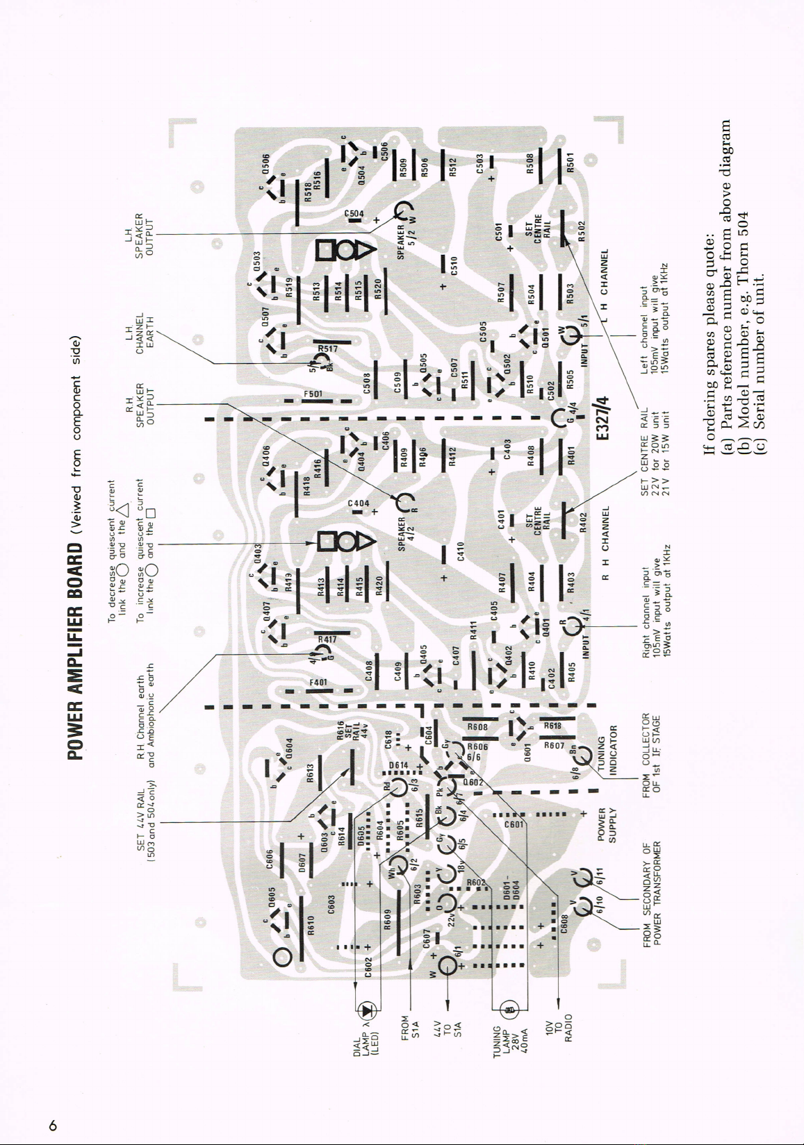
Description of complementary power output stage.
The collector of transistor Q402 is directly coupled to the bases ofa pair of complemen-
tary transistors Q404 and Q405 acting as drivers for the push-pull class Boutput pair,
Q406 and Q407. Direct coupling is used between the drivers and their corresponding
output transistors. The driver Q404 is effectively in the common collector mode and the
Q405 also in the common collector mode. Since the drive transistors Q404 and Q405
comprise an NPN and aPNP, they conduct on alternate half-cycles of signal, thereby
driving the output transistors likewise. There is no voltage gain, but power gain occurs
due to impedance changes, being the emitter-follower action of Q404/Q406 and Q405/
Q407 alternately. In the absence of signals, asteady current flows through Q404/Q406
and Q405/Q407 and their emitter load resistors. Asteady current also flowsin the driver
base resistors R406/R409 making Q406 base potential slightly positive with respect to
its emitter. Current through Q402 causes Q405 to beslightly negative with respectto the
centre rail. Thus Q404 and Q405 havea small forward bias which aids in the removal of
cross-over distortion in the output.
Transistor Q403 provides bias stabilisation for the driver stage output. This is achieved
by having the Ic of Q402 flow through Q403 and making biasing of Q406 and Q407 less
dependent on theIc of Q402. Effective thermal tracking is achieved by placing Q403 on
the same heat sink as the output devices (Q406 and Q407). Q403 acts as alow impedance
path for both signal and changes in d.c.
D.C. coupling is used in one feed-back loop to set up the d.c. working point of the output
transistors. This feed-back loop also keeps the distortion level low. In this regard, the
potential at the junction of R418/R419 is critical. If it is upset, severe clipping will result
in one half-cycle only at high signal levels. The junction of R418/R419 is returned via
R407 to the emitter of Q401. In addition to acting as an amplifier, Q401 compares the
voltage at the junction of R418/R419 with that at its emitter. For example, if the
mid-point starts to rise, Q401 emitter is driven more positive. Q401 collector voltage
rises causing acorresponding rise at Q402 base. Q402 collector falls, lowering the base
voltages on Q404 and Q405. As Q404 is an NPN transistor it will conduct less, with the
PNP transistor Q405 conducting more. This causes the centre rail voltage to fall
counter-acting the original drift upwards. Pre-set control R402 in avoltage divider
chain between the +44V rail and earth, sets the centre-rail (working point).
R420 and C409 in parallel across the ouput provide the necessary high frequency load to
the ouput transistors required due to the rising impedance ofthe loud speaker at high
frequencies. They also prevent destruction of Q406 and Q407 if speakers are discon-
nected.
R412 and R408 form an A.C. feed-back loop.
C402 acts as an RF bypass, as RF can present asubstantial signal level at this point.
C405 is the high frequency roll-off capacitor, ensuring high frequency stability.
C406 and C407 determine the maximum slewing rate possible at the output and hence
the upper frequency of the power band width.
R411 prevents high loop currents flowing in the ground line to which Aclass stages
Q401 and Q402 are connected.
C404 acts as abootstrapping capacitor and alsofilter for line hum.