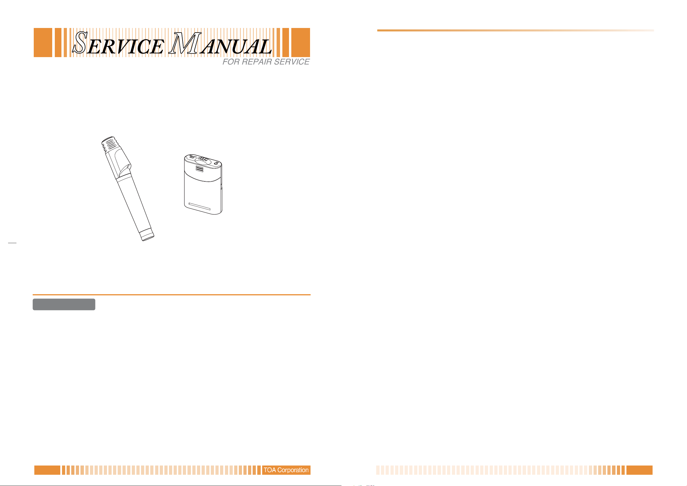
Toa IR-200M User manual

TABLE OF CONTENTS
Update history
IR-200M, IR-300M Y
1
No.833-73-809-10
INFRARED WIRELESS MICROPHONES
IR-200M, IR-300M Y
IR-200M
IR-300M
HS0905
NOTE ON REPAIR WORK SAFETY ......................................................................................................... 2
GENERAL DESCRIPTION ......................................................................................................................... 2
SPECIFICATIONS
• IR-200M ........................................................................................................................................... 3
• IR-300M ........................................................................................................................................... 3
NOMENCLATURE AND FUNCTIONS
• IR-200M ........................................................................................................................................... 4
• IR-300M ........................................................................................................................................... 4
DISASSEMBLING INSTRUCTIONS (IR-200M) ......................................................................................... 5
ADJUSTMENT PROCEDURE
• Measuring instruments to be used ................................................................................................... 6
• Connection diagram ......................................................................................................................... 6
• Adjustment points and input/output .................................................................................................. 7
• Adjustment and Check Method ........................................................................................................ 8
OPERATION FLOW
• At power on ...................................................................................................................................... 9
• From turning off the power switch to when the operation stops ....................................................... 9
TROUBLESHOOTING
• IR-200M ......................................................................................................................................... 10
• IR-300M ......................................................................................................................................... 10
BLOCK DIAGRAMS AND OPERATION DESCRIPTION
• IR-200M ......................................................................................................................................... 11
• IR-300M ......................................................................................................................................... 12
SCHEMATIC DIAGRAMS
• IR-200M
MAIN PCB ................................................................................................................................... 13
SUB PCB .................................................................................................................................... 14
• IR-300M
BATT PCB ................................................................................................................................... 15
IR PCB ........................................................................................................................................ 16
SW PCB ...................................................................................................................................... 17
MOUNTING DIAGRAMS AND PARTS LISTS
• IR-200M
MAIN PCB ................................................................................................................................... 18
SUB PCB .................................................................................................................................... 18
Charge contact PCB ................................................................................................................... 18
PARTS LIST ................................................................................................................................ 18
• IR-300M
BATT PCB ................................................................................................................................... 20
IR PCB ........................................................................................................................................ 20
SW PCB ...................................................................................................................................... 20
Charge contact PCB ................................................................................................................... 20
PARTS LIST ................................................................................................................................ 20
EXPLODED VIEWS AND PARTS LISTS
• IR-200M ......................................................................................................................................... 22
• IR-300M ......................................................................................................................................... 23
• Strap replacement procedure (IR-300M) ....................................................................................... 24
TABLE OF CONTENTS

IR-200M, IR-300M Y
2GENERAL DESCRIPTION 2NOTE ON REPAIR WORK SAFETY
The IR-200M (hand-held type) and IR-300M (hands-free type) infrared wireless microphones are
intended for speech applications and use unidirectional electret condenser microphone units featuring
high sensitivity and clear sound.
Follow the instructions below, both to prevent accidents when making repairs and to ensure post-repair
product safety.
Do not apply voltages other than those specified for the equipment or its compo-
nents.
Applying voltages other than the rated voltage could cause electrical breakdown or over-current, possi-
bly resulting in electric shock or fire.
Do not modify the design of circuit boards or other electronic elements.
Modifying circuit boards could cause electric shock or result in a fire hazard due to excessive heat
build-up. User modification automatically exempts the manufacturer from all personal and property lia-
bility caused by such modification, and the user who carried out such modification shall be solely
responsible for such accidents.
Since lead can become an environmental contaminant, this unit has been manufactured using solders
that contain no lead in the printed circuit board.
[While conventional solders are alloys of zinc and lead, lead-free solder is comprisend of an alterna-
tive alloy that contains no lead.]
NOTES
• Circuit boards using lead-free solder bear a lead-free solder designation. To maintain the integrity
of this designation, be sure to use lead-free solder when repairing such lead-free solder circuit
boards. Boards not marked with the lead-free solder designation may legally be serviced using
conventional solders.
• Because the melting point of lead-free solder (approximately 220°C) is 30°C-40°C higher than that
of conventional (lead-zinc alloy) solder, it tasks little longer to melt. It is recommended that a sol-
dering iron with controllable temperature be used and set to 20°C higher than would normally be
used with conventional solder.
Identifying printed circuit boards that use free-lead solder
Printed circuit boards that use lead-free solder have the following designation printed or stamped on
either side of the board.
• About lead-free solders
NOTE ON REPAIR WORK SAFETY GENERAL DESCRIPTION

IR-200M, IR-300M Y
3 3SPECIFICATIONS
• IR-200M
Note: The design and specifications are subject to change without notice for improvement.
• Accessories
Screwdriver (for setting) ............................. 1
Color label (6 colors) .................................. 1
• Optional products
Battery Charger : IR-200BC
Rechargeable battery: IR-200BT-2 (containing 2 pieces)
Battery IR-200BT rechargeable battery for the infrared wireless microphone
(2 pieces) or AA alkaline dry cell battery (2 pieces).
Current Consumption Typ. 250 mA (2.4 V, Power selector switch: N)
Typ. 340 mA (2.4 V, Power selector switch: H)
Wavelength 870 nm (AM: Brightness modulation)
Modulation Method Frequency modulation
Carrier Frequency Channel A: 3.100 MHz
Channel B: 3.350 MHz
Transmission Approx. 20 m or 65 ft (Power selector switch: H; In an unobstructed space.)
Distance Approx. 15 m or 50 ft (Power selector switch: N; In an unobstructed space.)
Tone Signal 32.768 kHz
Modulation Sensitivity ±4.8 kHz (1 kHz, when SPL of 84 dB is input)
Maximum Input Sound 120 dB SPL
Pressure
Microphone Unit Unidirectional electret condenser microphone
Frequency Response 100 Hz – 12 kHz
Preemphasis 300 μs
Battery Operation Time Approx. 8 hours (when the IR-200BT rechargeable battery for the infrared
wireless microphone is used; Power selector switch: N)
Approx. 6 hours (when the alkaline battery is used; Power selector switch: N)
Operating Temperature 0 to 40 °C (32 to 140 °F)
Operating Humidity 30 to 85% RH
Finish Control Section : ABS resin, metallic gray, 50% gloss, paint
Filter Section : Polycarbonate, optical cut filter
Dimensions ø37 x 241.8 (h) mm (ø1.46" x 9.52")
Weight 170 g or 0.37 lb (with alkaline batteries)
185 g or 0.41 lb (with dedicated rechargeable batteries)
Infrared Emitter
Note: The design and specifications are subject to change without notice for improvement.
• Accessories
Screwdriver (for setting) ............................. 1
Color label (6 colors) .................................. 1
• Optional products
Battery Charger : IR-200BC
Rechargeable battery: IR-200BT-2 (containing 2 pieces)
Battery IR-200BT rechargeable battery for the infrared wireless microphone
(2 pieces) or AA alkaline dry cell battery (2 pieces).
Current Consumption Typ. 250 mA (2.4 V, Power selector switch: N)
Typ. 340 mA (2.4 V, Power selector switch: H)
Wavelength 870 nm (AM: Brightness modulation)
Modulation Method Frequency modulation
Carrier Frequency Channel A: 3.100 MHz
Channel B: 3.350 MHz
Transmission Approx.
20 m or 65 ft (Power selector switch: H; In an unobstructed space.)
Distance Approx.
15 m or 50 ft (Power selector switch: N; In an unobstructed space.)
Tone Signal 32.768 kHz
Modulation Sensitivity ±4.8 kHz (1 kHz, when SPL of 84 dB is input)
Maximum Input Sound 120 dB SPL
Pressure
Input Sensitivity Adjustment range: –9 dB to 0 dB (factory-preset: 0 dB)
Adjustment
Microphone Unit Unidirectional electret condenser microphone
Frequency Response 100 Hz – 12 kHz
Preemphasis 300 μs
Input External microphone input (3.5 mm or 1/8" monaural mini jack)
Battery Operation Time Approx. 8 hours (when the IR-200BT rechargeable battery for the infrared
wireless microphone is used; Power selector switch: N)
Approx. 6 hours
(when the alkaline battery is used; Power selector switch: N)
Operating Temperature 0 to 40 °C (32 to 140 °F)
Operating Humidity 30 to 85% RH
Finish Control Section : ABS resin, metallic gray, 50% gloss, paint
Filter Section : Polycarbonate, optical cut filter
Dimensions 64 (w) x 91.3 (h) x 27.3 (d) mm (2.52" x 3.59" x 1.07")
Weight 130 g or 0.29 lb (with alkaline batteries & strap)
140 g or 0.31 lb (with dedicated rechargeable batteries & strap)
Infrared Emitter
• IR-300M
SPECIFICATIONS

IR-200M, IR-300M Y
4 4NOMENClATURE AND FUNCTIONS
• IR-200M • IR-300M
[Inside the battery case]
[Front] [Side]
78
2
3
3
4
5
6
1
1. Power switch
Turns on and off the microphone.
2. Battery indicator
Lights when the power switch (1) is turned on.
Continuously lights green while the battery is
fully charged, and gradually changes to red as
the battery becomes weaker.
3. Infrared emitter
Emits the infrared beam for communications.
4. Battery case
Contains the battery compartment. Be sure to
open and close the case correctly.
5. Color label attachment area
Attach optional color label to distinguish
between infrared wireless microphones.
6. Charging terminal
7. Power selector switch [PWR]
Switches the power level of the infrared beam
for communications.
8. Channel selector switch [CH]
Set the selector switch to the same channel as
that of the tuner.
1. Power switch / battery indicator
Turns on or off the microphone.
Turning on this switch causes its indicator to
come on, allowing it to also function as a battery
indicator.
This switch continuously lights green while the
battery is fully charged, and gradually changes
to red as the battery becomes weaker.
2. External microphone input terminal [MIC]
Used to connect a headset microphone or other
external microphone.
3. Infrared emitter
Transmits the infrared beam for communica-
tions.
4. Charging terminal
5. Neck strap
Used to suspend the infrared wireless micro-
phone from the neck.
6. Battery cover
Contains the battery compartment.
Be sure to open and close the cover correctly.
7. Color label attachment area
Attach optional color label to distinguish
between infrared wireless microphones.
8. Microphone level control
Used to adjust the input level when using an
external microphone.
9. Power selector switch
Switches the power level of the infrared beam
for communications.
10. Channel selector switch
Set the selector switch to the same channel as
that of the tuner.
5
[Front]
[Top]
[Rear]
2
3
4 6 7
1
[Inside of the battery cover]
9
8
10
Built-in microphone
NOMENCLATURE AND FUNCTIONS

IR-200M Y
5 5DISASSEMBLING INSTRUCTIONS
1. Take a firm hold of the rear case, turn the battery cover in the arrow direction, then remove the
battery cover.
2. Remove 1 screw circled on the photo, then remove the filter.
3. Remove 4 screws circled on the photo, then remove the rear case.
4. Remove 2 screws circled on the photo, then detach the BAT-PCB cover by holding down the tabs
while pulling up the section indicated by arrow.
Battery cover
Battery cover
Battery cover
Rear case
Rear case
Rear case
16
Battery cover
Battery cover
Battery cover
Rear case
Rear case
Rear case
Rear case
Rear case
Rear case
14
Rear case
Rear case
Rear case
Front case
Front case
Front case
Circled number suffixed to the part name corresponds to the item number in the parts list on the exploded
view page.
Filter
Filter
Filter
15
Filter
Filter
Filter
BAT-PCB cover
BAT-PCB cover
BAT-PCB cover
SUB PCB
SUB PCB
SUB PCB
Tabs
Tabs
Tabs
BAT-PCB cover
BAT-PCB cover
BAT-PCB cover
SUB PCB
SUB PCB
SUB PCB 13
5. Remove 1 screw securing the SUB PCB, disconnect 2 harnesses, then remove the SUB PCB and
Charge PCB assembly.
Note: Be careful not to over tighten the removed SUB PCB fixing screw when reassembling.
Note:
When reassembling, first insert the pins of the CN202 and CN203 on the MAIN PCB into the
pinholes of the CN101 and CN102 on the SUB PCB, then attach the contact lug (BATT+) into
the front case's slot. Be sure to insert the pins. Do not bend or fold the contact lug.
6. Remove 1 screw securing the MAIN PCB, and remove the MAIN PCB while slightly spreading the
tabs circled on the photo.
Note: Be careful not to over tighten the removed MAIN PCB fixing screw when reassembling.
SUB PCB
SUB PCB
SUB PCB
Harness
Harness
Harness
Harness
Harness
Harness
Screw
Screw
Screw
SUB PCB
SUB PCB
SUB PCB
Charge PCB
Charge PCB
assembly
assembly
Charge PCB
assembly
MAIN PCB
MAIN PCB
MAIN PCB
Pins
Pins
Pins
11
12
Tabs
Tabs
Tabs
MAIN PCB
MAIN PCB
MAIN PCB
Screw
Screw
Screw
MAIN PCB
MAIN PCB
MAIN PCB 11
SUB PCB
SUB PCB
SUB PCB
Pins
Pins
Pins
Front case
Front case
Front case
SUB PCB
SUB PCB
SUB PCB
Contact lug
Contact lug
Contact lug
Front case
Front case
Front case
DISASSEMBLING INSTRUCTIONS (IR-200M)

DISASSEMBLING INSTRUCTIONS
IR-200M, IR-300M Y
6 6
ADJUSTMENT PROCEDURE
7. Remove 3 screws circled on the photo, then remove the windscreen frame, switch knob, switch
knob fixing clamp, and LED light.
8. Remove 2 screws securing the windscreen frame to the neck joint. Detach the lower filter, then
remove the microphone element assembly and shock mount.
9. Detach the upper filter inserted between the windscreen net and microphone element holder using
tweezers.
10. When reassembling, proceed the steps in reverse order.
Switch knob fixing clamp
LED light.
LED light.
LED light.
Windscreen frame
Windscreen frame
Windscreen frame
Switch knob
Switch knob
Switch knob
LED light.
LED light.
LED light.
10
9
8
Windscreen frame
Windscreen frame
Windscreen frame
Switch knob fixing
Switch knob fixing
clamp
clamp
Switch knob fixing
clamp
Neck joint
Neck joint
Neck joint
Screws
Screws
Screws
Windscreen frame
Windscreen frame
Windscreen frame
Lower filter
Lower filter
Lower filter
Shock mount
Shock mount
Shock mount
Microphone
Microphone
element assembly
element assembly
Microphone
element assembly
1
5
3
4
6
Neck joint
Neck joint
Neck joint
Windscreen
Windscreen
frame
frame
Windscreen
frame
Upper filter
Upper filter
Upper filter
Windscreen frame
Windscreen frame
Windscreen frame 1
2
Upper filter
Upper filter
Upper filter
Windscreen frame
Windscreen frame
Windscreen frame
• Measuring instruments to be used
· Modulation analyzer : Band-width : 1.5 - 30 MHz or more
(Deviation meter, Frequency counter) Zi = 50 Ω
· Audio analyzer : Band-width : 20 Hz - 20 kHz or more
(Audio frequency generator and Distortion meter) Output impedance : 600 Ω
Input impedance : 100 Ωor more
· Oscilloscope: Band-width : 20 MHz or more
· Regulated DC power supply : 0 - 5 V DC
· DC ammeter : Full scale : 1 A or more
· DC voltmeter : Full scale : 10 V or more
· Spectrum analyzer : Band-width : 1.5 - 30 MHz or more, Zi = 50 Ω
• Connection diagram
Regulated
DC power
supply
Input
DC ammeter
Output
Oscilloscope
Spectrum
analyzer
PCB unit for the
IR-200M/300M
(Each PCB must be
connected as is actually used.)
Audio analyzer
AF oscillation output
600Ω
Over 10 μF
Ceramic
capacitor
1µF 16V
AF input
DC Power
RF output
Brightness
modulation level
+
Input
Modulation analyzer
AF output
RF input
DC voltmeter
Note: Use shielded cables for AF line and 50 Ω coaxial cables for RF line.
Current probe
PCB unit to be supplied as a service part is calibrated at the factory before shipment and further
adjustment is not required.
Adjust and check your microphone once the parts related to adjustment points on the PCB have been
replaced.
ADJUSTMENT PROCEDURE

IR-200M, IR-300M Y
7 7ADJUSTMENT PROCEDURE
• Adjustment points and input/output
· IR-200M
RF level control
· MAIN PCB (Component side)
· SUB PCB (Solder side)
· SUB PCB (Component side)
Vt terminal
Channel selector switch
AF input connector
TP2 : Check point for brightness
modulation level
TP1 : Check point for brightness
modulation level
Negative terminal of power supply
Check point for
RF measurement
Power selector switch
AF level control
Charge terminal connector
Positive terminal of power supply
Power switch
LH
ONOFF
· IR-300M
· SW PCB (Component side) · SW PCB (Solder side)
· IR PCB (Solder side)
· BATT PCB (Component side) · BATT PCB (Solder side)
Power switch
External microphone
input terminal
AF input connector AF level control
Negative terminal of power supply
Positive terminal of power supply
Vt terminal
Charge terminal connector
Channel selector switch
Power selector
switch
Microphone level control
TP2 : Check point for brightness
modulation level
TP1 : Check point for brightness
modulation level
Test point for RF measurement
RF level control
L
H
ON OFF

IR-200M, IR-300M Y
8 8ADJUSTMENT PROCEDURE
• Adjustment and Check Method
· IR-200M
(Conditions)
Room temperature : 15 - 35 °C (59 - 95 °F)
Power source : 2.4 ± 0.1 V DC
Power switch (SW102) : ON
Power selector switch (SW101) : "N" (Normal) position
Channel selector switch (SW100) : "B" position (Channel B)
Oscillation frequencies of Channels A and B are as follows.
Channel A: 3.100 MHz ± 20 kHz
Channel B: 3.350 MHz ± 20 kHz
Note: Setting the selector to the positions except “A” and “B” provides no output.
1. VCO check
1-1. Turn on the power switch (SW102) at Channel B.
Confirm that the current consumption is 250 ± 20 mA and LED100 lights green.
1-2. Connect the spectrum analyzer to the RF output (TP200), then confirm that the transmitting
frequency is 3.350 MHz ± 20 kHz and the output level is 90 dBμV or more.
2. Oscillation frequency check
Change the Channel selector switch (SW100) position, and turn OFF the power switch (SW102).
After more than 2 seconds, turn ON the power switch again.
Confirm the following signals are output depending on the selector switch positions.
Channel A position: 3.100 MHz ± 20 kHz
Positions except “A” and “B”:No output
(In this case, also confirm the power indicator alternately flashes green and red.)
3. Maximum frequency deviation adjustment
3-1. Connect the AF generator output of audio analyzer to the AF input (CN300), then apply
1 kHz /-6 dBV signal to the AF input.
3-2. Connect the modulation analyzer to the RF output (TP200), then adjust the AF level control (VR300) for
the frequency deviation of 40 ± 1 kHz. [Filter OFF, (p-p)/2]
3-3. Disconnect the modulation analyzer, and connect the spectrum analyzer to the RF output (TP200) again.
Then, confirm the tone signal (32.768 kHz) level is -32 dBC ± 3 dB.
4. Frequency response check
4-1. Connect the modulation analyzer to the RF output (TP200), and also the AF generator output of audio
analyzer to the AF input (CN300). Then, apply 400 Hz/-40 dBV signal to the AF input.
4-2. Confirm the modulation analyzer reads the following values when setting the audio frequencies to 100 Hz
and 8 kHz keeping the audio input level constant.
100Hz : -5.0±3.0dB
8kHz : +20.0±1.5dB
4-3. After the measurement above, disconnect the modulation analyzer from the RF output (TP200).
5. RF modulation level adjustment
5-1. Set the Channel selector switch (SW100) to "B" position, and turn OFF the power switch (SW102).
After more than 2 seconds, turn ON the power switch again.
5-2. Connect the oscilloscope to the check point (TP201) of brightness modulation level. Then, adjust the RF
level control (VR1) so that 3.350 MHz signal shows the following values.
DC voltage : 100 ± 10 mV
Carrier signal level : 150 mVp-p ± 10 mV
5-3. Connect the oscilloscope to the check point (TP202) of brightness modulation level, and confirm the
following value is obtained.
DC voltage : 100 ± 10 mV
Carrier signal level : 150 mVp-p ± 10 mV
5-4. Shift the Power selector switch (SW101) to "H" position, and confirm the following value is obtained at
TP202.
DC voltage : 100 ± 10 mV
Carrier signal level : 150 mVp-p ± 10 mV
Current consumption: 340 ± 20 mV
· IR-300M
(Conditions)
Room temperature : 15 - 35 ºC (59 - 95 ºF)
Power source : 2.4 ± 0.1 V DC
Power switch (SW300) : ON
Microphone level control (VR301) : “H” (Maximum) position
Power selector switch (SW201) : “N” (Normal) position
Channel selector switch (SW200) : “B” position (Channel B)
Oscillation frequencies of Channels A and B are as follows.
Channel A: 3.100 MHz ± 20 kHz
Channel B: 3.350 MHz ± 20 kHz
Note: Setting the selector to the positions except “A” and “B” provides no output.
1. VCO check
1-1. Turn on the power switch (SW300) at Channel B.
Confirm that the current consumption is 250 ± 20 mA and the power switch (SW300) lights green.
1-2. Connect the spectrum analyzer to the RF output (TP201), then confirm that the transmitting frequency is
3.350 MHz ± 20 kHz and the output level is 90 dBμV or more.
2. Oscillation frequency check
Change the Channel selector switch (SW200) position, and turn OFF the power switch (SW300).
After more than 2 seconds, turn ON the power switch again.
Confirm the following signals are output depending on the selector switch positions.
Channel A position: 3.100 MHz ± 20 kHz
Positions except “A” and “B”: No output
(In this case, also confirm the power switch alternately flashes green and red.)
3. Maximum frequency deviation adjustment
3-1. Connect the AF generator output of audio analyzer to the AF input (CN300), then apply 1 kHz /-15 dBV
signal to the AF input.
3-2. Connect the modulation analyzer to the RF output (TP201), then adjust the AF level control (VR300) for
the frequency deviation of 40 ± 1 kHz. [Filter OFF, (p-p)/2]
3-3. Disconnect the modulation analyzer, and connect the spectrum analyzer to the RF output (TP201) again.
Then, confirm the tone signal (32.768 kHz) level is -32 dBC ± 3 dB with the Microphone level control
(VR301) set to "L" (Minimum) position.
4. Frequency response check
4-1. Connect the modulation analyzer to the RF output (TP201), and also the AF generator output of audio
analyzer to the AF input (CN300). Then, apply 400 Hz/-52 dBV signal to the AF input.
4-2. Confirm the modulation analyzer reads the following values when setting the audio frequencies to 100 Hz
and 8 kHz keeping the audio input level constant.
100Hz : -5.0±3.0dB
8kHz : +20.0±1.5dB
4-3. After the measurement above, disconnect the modulation analyzer from the RF output (TP201).
5. RF modulation level adjustment
5-1. Set the Channel selector switch (SW200) to "B" position, and turn OFF the power switch (SW300).
After more than 2 seconds, turn ON the power switch again.
5-2. Connect the oscilloscope to the check point (TP203) of brightness modulation level. Then, adjust the RF
level control (VR1) so that 4.725 MHz signal shows the following values.
DC voltage : 100 ± 10 mV
Carrier signal level : 150 mVp-p ± 10 mV
5-3. Connect the oscilloscope to the check point (TP204) of brightness modulation level, and confirm the fol-
lowing value is obtained.
DC voltage : 100 ± 10 mV
Carrier signal level : 150 mVp-p ± 10 mV
5-4. Shift the Power selector switch (SW201) to "H" position, and confirm the following value is obtained at
TP204.
DC voltage : 100 ± 10 mV
Carrier signal level : 150 mVp-p ± 10 mV
Current consumption: 340 ± 20 mV

OPERATION FLOW
IR-200M, IR-300M Y
9 9TROUBLESHOOTING
[Common to the IR-200M and IR-300M]
Turn on the power switch.
Infrared emitting LED starts to emit light.
The DC/DC converter operates, and its circuit
voltage rises to 5.0 V.
Tone signals and audio muting are reset.
Turn off the power switch.
(Leave FET Q102 for the power switch ON.)
Tone signals and audio muting are turned on.
Operation stop process starts.
Power turns off.
All operation stops.
PLL comparison frequency and channel are set.
(Transmits the data to decide dividing ratio to
the PLL IC M4.)
The CPU is reset when the circuit voltage rises
to 2.6 V, activating Start-up clock (6 MHz), and
reset voltage turns to H.
Infrared emitting LED stops to emit light.
• At power on
• From turning off the power switch to when the operation stops
First, check and remedy the problem you are facing referring to the table below. If the symptom still does not
improve, follow the flow chart on pages 10 to find the possible cause.
• Charge using the IR-200BC
Battery Charger.
[Operating on dry cell batteries]
• Battery polarities not correct.
• Batteries exhausted.
Symptom Possible cause Remedy
Battery indicator does not
light even if the power switch
is turned on.
[Operating on rechargeable batteries]
• Battery polarities not correct.
• Specified battery not used.
• Battery not charged.
• Reinsert batteries correctly.
• Replace the batteries with the IR-
200BT rechargeable batteries for
the infrared wireless microphone.
• Charge using IR-200BC Battery
Charger.
• Reinsert batteries correctly.
• Replace with new ones.
When the power switch is
turned on, the battery
indicator lights red.
[Operating on dry cell batteries]
• Batteries exhausted. • Replace with new ones.
[Operating on rechargeable batteries]
• Battery discharged.
When the power switch is
turned on, the battery
indicator alternately flashes
green and red.
• Channel selector switch not set
correctly to an indicated position. • Perform channel settings correctly.
Infrared wireless tuner's
reception indicator does not
light (no signal received)
even with the power switch
turned on.
• Channel set for infrared wireless
microphone not identical to the
tuner.
• Reset the infrared microphone to
the same channel as the tuner.
Interferes with other infrared
microphone being used
simultaneously.
• Two infrared wireless microphones
set to the same channel. • Set channels correctly.
• Infrared wireless microphone
used too close to the tuner. • Keep the infrared microphone at
least 50 cm (19.69") away from
the infrared tuner.
OPERATION FLOW TROUBLESHOOTING

IR-200M, IR-300M Y
10 10TROUBLESHOOTING
• IR-200M
Microphone audio signals
not output.
DC/DC converter's
output voltage is 5.0 V.
(C113 + terminal)
Reset terminal
of the CPU is maintained at H.
(TP105, Pin No. 8 of
the M100)
Yes
Yes
Yes
Clock
(6 MHz) is oscillating.
(Pin No. 3 of the
M100)
No DC/DC converter (M102) or power
switch (SW102) may be failed.
No
Reset circuit (M101) may be failed.
No Clock oscillator (X100, M100) may
be failed.
Yes
VCO is oscillating.
(TP5)
No VCO circuit (Q2) or buffer amplifier
(Q4) may be failed.
Yes
Transmitting
frequency is normal.
No Clock oscillator (X100) or PLL
synthesizer (M4) may be failed.
Yes
RF output is normal.
(TP200, TP201, TP202)
No RF amplifier (M200, M201, M202)
may be failed.
Audio frequency circuit
(M300, M302) may be failed.
Yes
Infrared
emitting LED is emitting light.
(LED200 - 204)
No LED driver (Q202, Q203, Q205, Q206)
or LED bias (Q200, Q201) may be failed.
Yes
Signals
are received by the
infrared tuner.
No Tone oscillation circuit (X300, M303, M304)
or AF mute circuit (M3) may be failed
• IR-300M
DC/DC converter's
output voltage is 5.0 V.
(C113 + terminal)
Reset terminal
of the CPU is maintained at H.
(TP105 and Pin No. 8 of
the M100)
Yes
Yes
Yes
Clock
(6 MHz) is oscillating.
(Pin No. 3 of the
M100)
No DC/DC converter (M102) or power
switch (SW300) may be failed.
No
Reset circuit (M101) may be failed.
No Clock oscillator (X100, M100) may
be failed.
Yes
VCO is oscillating.
(TP5)
No VCO circuit (Q2) or buffer amplifier
(Q4) may be failed.
Yes
Transmitting
frequency is normal.
No Clock oscillator (X100) or PLL
synthesizer (M4) may be failed.
Yes
RF output is normal.
(TP201, TP203, TP204)
No RF amplifier (M200, M201, M202)
may be failed.
Audio frequency circuit
(M300, M302) may be failed.
Yes
Infrared
emitting LED is emitting light.
(LED200 - 205)
No LED driver (Q202, Q205, Q206, Q207) or
LED bias (Q200, Q201) may be failed.
Yes
Signals
are received by the
infrared tuner.
No Tone oscillation circuit (X300, M303, M304)
or AF mute circuit (M3) may be failed.
Microphone audio signals
not output.

1
A
B
C
D
E
F
G
H
23 654 789 11121310
I
IR-200M Y
11 11
Low frequency section
RF and IR section
PLL synthesizer section
Power supply section
Electret condenser
microphone
Bias circuit
R300, 302
Microphone amplifier
M302(1/2)
Pre-emphasis
M302(1/2)
Low-pass filter
Q300
Buffer amplifier
Q4
RF amplifier
M200
LED driver
M201
Q202, 203
Infrared emitting LED
LED200-202
Infrared emitting LED
LED203, 204, 1
Power selector switch
SW101
Green Red
IR bias control
Battery voltage monitor Reset
Battery checker
LED100
LED driver
M202
Q205, 206
Ripple filter
Q5
Loop filter
IR bias control
Q200, 201
Drive current control
Q204, 207
AF level control
VR300
RF level control
VR1
VCO
Q2, 3, 5
D1, 5
Voltage detector
M101
Compressor
M300
DC-DC converter
M102, Q101, D104
Tone oscillator
M303, 304, X300
Channel selector switch
SW100
CPU (control)
M100
Clock
X100
6.000MHz
DC 5.0V
DC 5.0V
AF mute
M3
DC 2.4V
OFF detection
Q100
M
Circuit switch
Q102, 103, 105
Circuit voltage
DC 5.0V
Power switch
SW102
Circuit voltage
DC 2.4V
Battery
terminal
Charging
terminal
PLL
M4
Amplifies signals
from microphone
element.
Amplifies high frequency
components of audio
signals at time constant
of 300 μs.
Serves as a buffer
and cuts 15 kHz or
higher frequencies.
Logarithmic-
compresses audio
signals to 2:1.
Supplies power to
microphone
element.
Oscillation circuit
uses C-MOS
inverter.
Performs system control,
frequency data transmission to
PLL, and battery voltage monitor.
Serves as an
impedance converter
as well as a buffer.
Oscillates transmitting
frequency in
conjunction with PLL.
Amplifies
RF signals
from VCO.
Frequency-divides and phase-compares each
output from reference oscillator (6 MHz) and
VCO, generating pulses depending on the phase
difference.Comparison frequency is 25 kHz.
Low-pass filter to produce
control voltage (DC) for
VCO by using pulses
generated from PLL IC.
Controls power
supply to Infrared
emitting LED.
Converts voltage of RF signals into
current, and amplitude-modulates
infrared lights generated from
infrared emitting LED.
Switches LED drive
current to output infrared
lights in High or Normal
mode.
Creates 5 V DC
from battery
voltage.
Turns on and supplies 5 V DC to the entire circuit to operate when the power
switch is turned on. Once the CPU starts operating, it controls the circuit switch.
The circuit switch turns off through OFF control and termination operations
when the power switch is turned off. It also turns off when the battery voltage
drops to 2 V or less, disconnecting the following circuits and preventing
over-discharge of battery.
• IR-200M
BLOCK DIAGRAMS AND OPERATION DESCRIPTION

1
A
B
C
D
E
F
G
H
23 654 789 11121310
I
IR-300M Y
12 12BLOCK DIAGRAMS AND OPERATION DESCRIPTION
Low frequency section
PLL synthesizer section
RF and IR section
Power supply section
Microphone amplifier
M302(1/2)
Pre-emphasis
M302(1/2)
Low-pass filter
Q300
Buffer amplifier
Q4
RF amplifier
M200
LED driver
M201
Q202, 205
Infrared emitting LED
LED200-202
Infrared emitting LED
LED203-205
Power selector switch
SW201
Battery checker
LED driver
M202
Q206, 207
Ripple filter
Q5
Loop filter
IR bias control
Q200, 201
Drive current control
Q203, 208
AF level control
VR300
RF level control
VR1
VCO
Q2, 3, 6
D1, 5
Voltage detector
M101
Compressor
M300
DC-DC converter
M102, Q101, D104
Tone oscillator
M303, 304, X300
Channel selector switch
SW200
Clock
X100
6.000MHz
DC 5.0V
AF mute
M3
DC 2.4V
Circuit switch
Q102, 103, 105
Power switch
SW300
PLL
M4
Electret condenser
microphone
External input terminal
Bias circuit
R300, 302
DC 5.0V
M
IR bias control
CPU (control)
M100
Battery voltage monitor Reset
Battery
terminal
Charging
terminal
OFF detection
Q106, 107
Circuit voltage
DC 5.0V
Circuit voltage
DC 2.4V
Green Red
Connecting external
microphone turns off built-in
electret microphone.
Supplies power to
the condenser
microphone element.
Amplifies signals
from microphone
element.
Logarithmic-
compresses audio
signals to 2:1.
Oscillation circuit
uses C-MOS
inverter.
Amplifies high frequency
components of audio
signals at time constant
of 300 μs.
Serves as a buffer
and cuts 15 kHz or
higher frequencies.
Oscillates transmitting
frequency in
conjunction with PLL.
Frequency-divides and phase-compares each
output from reference oscillator (6 MHz) and
VCO, generating pulses depending on the phase
difference.Comparison frequency is 25 kHz.
Low-pass filter to produce
control voltage (DC) for
VCO by using pulses
generated from PLL IC.
Serves as an
impedance converter
as well as a buffer.
Amplifies
RF signals
from VCO.
Switches LED drive
current to output infrared
lights in High or Normal
mode.
Performs system control,
frequency data transmission to
PLL, and battery voltage monitor.
Creates 5 V DC
from battery
voltage.
Turns on and supplies 5 V DC to the entire circuit to operate when the power
switch is turned on. Once the CPU starts operating, it controls the circuit switch.
The circuit switch turns off through OFF control and termination operations
when the power switch is turned off. It also turns off when the battery voltage
drops to 2 V or less, disconnecting the following circuits and preventing
over-discharge of battery.
Controls power
supply to Infrared
emitting LED.
Converts voltage of RF signals into
current, and amplitude-modulates
infrared lights generated from
infrared emitting LED.
• IR-300M

1
A
B
C
D
E
F
G
H
23 654 789 11121310
I
IR-200M Y
13 13
To CN202 of
SUB PCB
To CN203 of
SUB PCB
To CN200 of
SUB PCB
AF mute
PLL
Ripple filter
VCO
Buffer amplifier
RF level
control
Power selector switch
OFF detection
Power switch
Channel selector
switch
Voltage
detector
Clock
Battery checker
CPU
(control)
dummy
1608Jumper
• IR-200M
· MAIN PCB
SCHEMATIC DIAGRAMS
SCHEMATIC DIAGRAMS

1
A
B
C
D
E
F
G
H
23 654 789 11121310
I
IR-200M Y
14 14SCHEMATIC DIAGRAMS
6dB ATT
To CN100 of
MAIN PCB
To Charge PCB
assembly
To Microphone
element assembly
Microphone
amplifier
Pre-emphasis
AF level control
Low-pass filter
Compressor
Tone oscillator
Electret condenser
microphone
To CN102 of
MAIN PCB
To CN101 of
MAIN PCB
Drive current control
LED driver
Infrared emitting LED
LED driver
RF amplifier
IR bias control
Drive current control
300μs
· SUB PCB

1
A
B
C
D
E
F
G
H
23 654 789 11121310
I
IR-200M Y
18 18MOUNTING DIAGRAMS AND PARTS LISTS
• IR-200M
· MAIN PCB (Part Code : 700-04-267-80)
· SUB PCB (Part Code : 700-04-267-80)
Viewed from parts mounting side Viewed from Conductor side
· Charge contact PCB (Part Code : 700-04-219-50)
The MAIN PCB and SUB PCB are supplied in set.
Caution
Charge contact PCB is supplied with the charge plates
and harnesses attached.
Caution
Viewed from parts mounting side
Viewed from Conductor side
Designator Part Code Description
BATT 124-04-438-40 CONTACT,IR200M (-)
BATT+ 124-04-217-9B CONTACT(+),BATTERY,WM1200
C1 113-40-794-7X GRM185B30J105KE25D
C10 113-40-664-5X CAPACITOR,1608 50V 10NF TAP
C11 113-40-795-6X GRM21BB30J106KE18L
C12 113-40-793-0X GRM188B30J475KE18D
C13 113-40-793-0X GRM188B30J475KE18D
C14 113-40-795-6X GRM21BB30J106KE18L
C15 113-40-664-5X CAPACITOR,1608 50V 10NF TAP
C16 113-40-794-7X GRM185B30J105KE25D
C17 113-40-794-7X GRM185B30J105KE25D
C18 dummy
C19 113-40-640-5X CAPACITOR,U0603C101JNT
C20 113-40-793-0X GRM188B30J475KE18D
C21 dummy
C22 113-40-747-5X CAPACITOR,C 25V 0.1MF B T
C23 113-40-647-4X CAPACITOR,1608 50V 390PF NPO J
C24 113-40-646-1X U0603C331JNT
C25 113-40-793-0X GRM188B30J475KE18D
C26 dummy
C28 113-40-664-5X CAPACITOR,1608 50V 10NF TAP
C29 dummy
C30 113-40-630-6X CAPACITOR,U0603C150JNT
C31 113-40-794-7X GRM185B30J105KE25D
C32 113-40-644-1X CAPACITOR,U0603C221JNT
C33 113-40-644-1X CAPACITOR,U0603C221JNT
C34 113-40-664-5X CAPACITOR,1608 50V 10NF TAP
C35 113-40-652-0X CAPACITOR,U0603C102JNT
C36 113-40-664-5X CAPACITOR,1608 50V 10NF TAP
C37 113-40-621-0X U0603C030CNT
C38 113-40-664-5X CAPACITOR,1608 50V 10NF TAP
C39 113-40-664-5X CAPACITOR,1608 50V 10NF TAP
C41 113-40-632-0X U0603C220JNT
C100 113-40-630-6X CAPACITOR,U0603C150JNT
C101 113-40-626-5X U0603C080DNT
C102 113-40-652-0X CAPACITOR,U0603C102JNT
C103 113-40-747-5X CAPACITOR,C 25V 0.1MF B T
C104 113-40-747-5X CAPACITOR,C 25V 0.1MF B T
C105 113-40-795-6X GRM21BB30J106KE18L
C106 113-40-699-1X CAPACITOR,16V 1608 220NF X7R K
C107 113-13-570-3X CAPACITOR,267E 10V 100MF(M)B
C108 113-13-570-3X CAPACITOR,267E 10V 100MF(M)B
C109 113-40-699-1X CAPACITOR,16V 1608 220NF X7R K
C111 113-40-699-1X CAPACITOR,16V 1608 220NF X7R K
C112 113-13-570-3X CAPACITOR,267E 10V 100MF(M)B
C113 113-13-570-3X CAPACITOR,267E 10V 100MF(M)B
C200 113-40-794-7X GRM185B30J105KE25D
C201 113-40-794-7X GRM185B30J105KE25D
C202 dummy
C203 dummy
C204 dummy
C205 113-13-570-3X CAPACITOR,267E 10V 100MF(M)B
C206 113-40-794-7X GRM185B30J105KE25D
C207 113-40-747-5X CAPACITOR,C 25V 0.1MF B T
C208 113-40-747-5X CAPACITOR,C 25V 0.1MF B T
C209 dummy
C210 113-40-794-7X GRM185B30J105KE25D
C211 113-40-794-7X GRM185B30J105KE25D
C213 dummy
C214 113-40-794-7X GRM185B30J105KE25D
C215 113-13-570-3X CAPACITOR,267E 10V 100MF(M)B
C216 113-40-794-7X GRM185B30J105KE25D
C217 113-13-570-3X CAPACITOR,267E 10V 100MF(M)B
C218 113-40-794-7X GRM185B30J105KE25D
C219 113-40-794-7X GRM185B30J105KE25D
C220 113-40-794-7X GRM185B30J105KE25D
C221 113-40-794-7X GRM185B30J105KE25D
C222 113-40-794-7X GRM185B30J105KE25D
C224 113-40-794-7X GRM185B30J105KE25D
C225 113-40-794-7X GRM185B30J105KE25D
· PARTS LIST
MOUNTING DIAGRAMS AND PARTS LISTS

IR-200M Y
19 19MOUNTING DIAGRAMS AND PARTS LISTS
Designator Part Code Description
C226 113-40-794-7X GRM185B30J105KE25D
C227 dummy
C301 113-40-652-0X CAPACITOR,U0603C102JNT
C302 dummy
C303 113-40-793-0X GRM188B30J475KE18D
C304 113-40-640-5X CAPACITOR,U0603C101JNT
C305 113-40-747-5X CAPACITOR,C 25V 0.1MF B T
C306 113-40-652-0X CAPACITOR,U0603C102JNT
C307 dummy
C308 113-40-795-6X GRM21BB30J106KE18L
C309 113-40-646-1X U0603C331JNT
C310 113-40-793-0X GRM188B30J475KE18D
C312 113-40-793-0X GRM188B30J475KE18D
C313 dummy
C314 112-80-300-3X WIRE,JUMPER
C315 113-40-795-6X GRM21BB30J106KE18L
C316 113-40-794-7X GRM185B30J105KE25D
C317 113-40-632-0X U0603C220JNT
C318 112-80-300-3X WIRE,JUMPER
C319 113-40-795-6X GRM21BB30J106KE18L
C320 113-40-652-0X CAPACITOR,U0603C102JNT
C321 113-40-640-5X CAPACITOR,U0603C101JNT
C322 113-40-425-8X CAPACITOR 0.047PF 50V
C323 113-40-795-6X GRM21BB30J106KE18L
C324 113-40-664-5X CAPACITOR,1608 50V 10NF TAP
C325 dummy
C326 113-40-793-0X GRM188B30J475KE18D
C327 113-40-793-0X GRM188B30J475KE18D
C328 113-40-631-7X CAPACITOR,U0603C180JNT
C329 113-40-631-7X CAPACITOR,U0603C180JNT
C330 113-40-652-0X CAPACITOR,U0603C102JNT
C331 113-40-644-1X CAPACITOR,U0603C221JNT
C332 113-40-652-0X CAPACITOR,U0603C102JNT
C333 113-40-640-5X CAPACITOR,U0603C101JNT
C334 113-40-664-5X CAPACITOR,1608 50V 10NF TAP
C335 113-40-664-5X CAPACITOR,1608 50V 10NF TAP
C336 113-40-663-8X CAPACITOR,50V 8200PF X7R(K)
CHARGE1, 2 124-04-439-10 CONTACT,IR200M CHARGE (-)
CN100 123-36-094-2X CONNECTOR, AXN320C038P
CN101 123-36-645-00 CONNECTOR,MX-2-4-2P HEADER
CN102 123-36-645-00 CONNECTOR,MX-2-4-2P HEADER
CN200 123-36-095-1X CONNECTOR, AXN420C530P TAPING
CN201 123-36-648-9X CONNECTOR,BM03B-ACHSS-GAN-TF
CN202 123-36-646-10 CONNECTOR,ME-2-1-2P SOCKET
CN203 123-36-646-10 CONNECTOR,ME-2-1-2P SOCKET
CN300 123-36-647-4X CONNECTOR,BM02B-ACHSS-GAN-TF
D1 111-03-981-2X VARICAP, HVU17 TRF-T
D2 dummy
D4 111-03-987-0X DIODE,DCG010 TAPING
D5 111-23-048-4X DIODE,1SS314 TPH3T
D100 111-23-041-1X IC, RB501V-40 TE-17
D101 111-23-041-1X IC, RB501V-40 TE-17
D102 111-23-041-1X IC, RB501V-40 TE-17
D103 111-23-041-1X IC, RB501V-40 TE-17
D104 111-23-207-5X D1FH3(5063) TAPING
D105 111-03-664-6X DIODE, SB05-05CP *
L1 114-19-975-3X COIL,NLV32T-220J-PF
L2 114-19-992-8X COIL, NLV32T-270J-PF G T
L100 114-29-023-4X CDRH4D18C-100NC
L101 114-19-412-7X COIL, LQH3C100K04
L200 112-80-300-3X WIRE,JUMPER
L201 112-80-300-3X WIRE,JUMPER
L202 114-05-256-4X COIL,LQH43CN100K03L
L203 112-80-300-3X WIRE,JUMPER
L301 112-80-300-3X WIRE,JUMPER
L302 112-80-300-3X WIRE,JUMPER
LED1 111-08-374-50 LED, LN870F-04U(IR)
LED100 111-08-427-8X LED,BRBG1204W-TR
LED200 111-08-374-50 LED, LN870F-04U(IR)
LED201 111-08-374-50 LED, LN870F-04U(IR)
Designator Part Code Description
LED202 111-08-374-50 LED, LN870F-04U(IR)
LED203 111-08-374-50 LED, LN870F-04U(IR)
LED204 111-08-374-50 LED, LN870F-04U(IR)
M3 111-10-238-1X IC, TC7S66FU CM0S TE85L
M4 111-26-029-2X IC, BU2630FV T
M100 111-12-428-60 IC.TMP86FH47ADUG IR200M V1.10
M101 111-26-122-4X R3111N261A TAPING
M102 111-26-174-1X IC,XC6367A501MRN
M200 111-26-026-7X IC, LMH6642MF T
M201 111-26-026-7X IC, LMH6642MF T
M202 111-26-026-7X IC, LMH6642MF T
M300 111-26-058-2X IC,TK10690MTL-G
M302 111-06-842-1X IC,NJM2115V T
M303 111-10-242-0X IC TC7SU04FU TE85L CMOS
M304 111-10-201-3X TC7S04FU
Q2 111-02-405-6X TRANSISTOR, 2SC4081S
Q3 111-01-225-3X TRANSISTOR, 2SA1576S
Q4 111-02-405-6X TRANSISTOR, 2SC4081S
Q5 111-02-377-8X TRANSISTOR, 2SC4555
Q6 111-02-450-6X TRANSISTOR, KTC4075(GR) T
Q100 111-02-450-6X TRANSISTOR, KTC4075(GR) T
Q101 111-07-115-5X XP161A1355PRN TAPING
Q102 111-07-125-0X TRANSISTOR,MCH3319
Q103 111-02-450-6X TRANSISTOR, KTC4075(GR) T
Q105 111-02-450-6X TRANSISTOR, KTC4075(GR) T
Q200 111-01-196-4X TRANSISTOR, 2SA1362(GR)
Q201 111-02-450-6X TRANSISTOR, KTC4075(GR) T
Q202 111-07-102-1X FET, 2SK3074 T
Q203 111-07-102-1X FET, 2SK3074 T
Q204 111-02-450-6X TRANSISTOR, KTC4075(GR) T
Q205 111-07-102-1X FET, 2SK3074 T
Q206 111-07-102-1X FET, 2SK3074 T
Q207 111-02-450-6X TRANSISTOR, KTC4075(GR) T
Q300 111-02-405-6X TRANSISTOR, 2SC4081S
R1 112-80-300-3X WIRE,JUMPER
R11 112-80-385-8X RESISTOR, 10K OHM 5%3/100
R12 112-80-385-8X RESISTOR, 10K OHM 5%3/100
R13 112-80-401-9X RESISTOR, 47K OHM 5%3/100
R14 112-80-401-9X RESISTOR, 47K OHM 5%3/100
R15 112-80-393-1X RESISTOR, 22K OHM 5%3/100
R16 112-80-391-3X RESISTOR 18K OHM 5%3/100
R17 112-80-371-7X RESISTOR, 2.7K OHM
R18 112-80-409-9X RESISTOR, 100K OHM 5%3/100
R19 112-80-385-8X RESISTOR, 10K OHM 5%3/100
R20 112-80-300-3X WIRE,JUMPER
R21 112-80-373-5X RESISTOR, 3.3K OHM 5%3/100
R22 112-80-397-1X RESISTOR, 33K OHM 5%3/100
R23 112-80-421-7X RESISTOR 330K OHM 5%3/100
R24 112-80-367-0X RESISTOR 1.8K OHM
R25 112-80-353-7X RESISTOR,470 OHM 5%3/100
R26 112-80-393-1X RESISTOR, 22K OHM 5%3/100
R27 112-80-385-8X RESISTOR, 10K OHM 5%3/100
R28 112-80-393-1X RESISTOR, 22K OHM 5%3/100
R29 112-80-361-2X RESISTOR,1K OHM 5%3/100
R30 112-80-421-7X RESISTOR 330K OHM 5%3/100
R31 112-80-353-7X RESISTOR,470 OHM 5%3/100
R32 112-80-365-6X RESISTOR 1.5K OHM 5%3/100
R33 112-80-337-7X RESISTOR,100 OHM 5%3/100
R34 112-80-365-6X RESISTOR 1.5K OHM 5%3/100
R35 112-80-369-2X RESISTOR, 2.2K OHM 5%3/100
R36 112-80-365-6X RESISTOR 1.5K OHM 5%3/100
R37 112-80-300-3X WIRE,JUMPER
R38 112-80-300-3X WIRE,JUMPER
R39 112-80-300-3X WIRE,JUMPER
R40 112-80-373-5X RESISTOR, 3.3K OHM 5%3/100
R41 112-80-361-2X RESISTOR,1K OHM 5%3/100
R100 112-80-409-9X RESISTOR, 100K OHM 5%3/100
R101 112-80-337-7X RESISTOR,100 OHM 5%3/100
R103 112-80-357-7X RESISTOR 680 OHM 5%3/100
R105 112-80-385-8X RESISTOR, 10K OHM 5%3/100
Designator Part Code Description
R106 112-80-385-8X RESISTOR, 10K OHM 5%3/100
R107 112-80-385-8X RESISTOR, 10K OHM 5%3/100
R108 112-80-385-8X RESISTOR, 10K OHM 5%3/100
R109 112-80-385-8X RESISTOR, 10K OHM 5%3/100
R110 112-80-385-8X RESISTOR, 10K OHM 5%3/100
R111 112-80-377-5X RESISTOR, 4.7K OHM 5%3/100
R112 112-80-385-8X RESISTOR, 10K OHM 5%3/100
R113 112-80-385-8X RESISTOR, 10K OHM 5%3/100
R114 dummy
R115 112-80-385-8X RESISTOR, 10K OHM 5%3/100
R116 112-80-385-8X RESISTOR, 10K OHM 5%3/100
R117 dummy
R118 112-80-300-3X WIRE,JUMPER
R119 112-80-385-8X RESISTOR, 10K OHM 5%3/100
R120 112-80-385-8X RESISTOR, 10K OHM 5%3/100
R121 112-80-377-5X RESISTOR, 4.7K OHM 5%3/100
R122 112-80-377-5X RESISTOR, 4.7K OHM 5%3/100
R123 112-80-300-3X WIRE,JUMPER
R124 dummy
R125 dummy
R126 dummy
R127 112-80-385-8X RESISTOR, 10K OHM 5%3/100
R128 dummy
R129 112-80-409-9X RESISTOR, 100K OHM 5%3/100
R130 dummy
R131 112-80-393-1X RESISTOR, 22K OHM 5%3/100
R132 112-80-361-2X RESISTOR,1K OHM 5%3/100
R133 112-80-369-2X RESISTOR, 2.2K OHM 5%3/100
R134 112-80-385-8X RESISTOR, 10K OHM 5%3/100
R135 112-80-333-7X RESISTOR 68 OHM 5%
R136 112-80-409-9X RESISTOR, 100K OHM 5%3/100
R137 112-80-385-8X RESISTOR, 10K OHM 5%3/100
R138 112-80-409-9X RESISTOR, 100K OHM 5%3/100
R139 112-80-385-8X RESISTOR, 10K OHM 5%3/100
R140 112-80-409-9X RESISTOR, 100K OHM 5%3/100
R142 112-80-300-3X WIRE,JUMPER
R143 112-80-385-8X RESISTOR, 10K OHM 5%3/100
R144 112-80-385-8X RESISTOR, 10K OHM 5%3/100
R145 112-80-385-8X RESISTOR, 10K OHM 5%3/100
R146 112-80-385-8X RESISTOR, 10K OHM 5%3/100
R147 112-80-385-8X RESISTOR, 10K OHM 5%3/100
R148 112-80-385-8X RESISTOR, 10K OHM 5%3/100
R149 112-80-385-8X RESISTOR, 10K OHM 5%3/100
R150 112-80-385-8X RESISTOR, 10K OHM 5%3/100
R151 dummy
R152 112-80-409-9X RESISTOR, 100K OHM 5%3/100
R153 112-80-413-0X RESISTOR 150K OHM 5%3/100
R200 dummy
R201 112-80-385-8X RESISTOR, 10K OHM 5%3/100
R202 112-80-385-8X RESISTOR, 10K OHM 5%3/100
R203 112-80-347-6X RESISTOR 270 OHM 5%3/100
R204 112-80-373-5X RESISTOR, 3.3K OHM 5%3/100
R205 112-80-347-6X RESISTOR 270 OHM 5%3/100
R206 112-80-385-8X RESISTOR, 10K OHM 5%3/100
R207 112-80-385-8X RESISTOR, 10K OHM 5%3/100
R208 112-80-361-2X RESISTOR,1K OHM 5%3/100
R209 112-80-345-2X RESISTOR,220 OHM 5%3/100
R210 112-80-401-9X RESISTOR, 47K OHM 5%3/100
R211 112-80-300-3X WIRE,JUMPER
R212 112-80-300-3X WIRE,JUMPER
R213 112-80-300-3X WIRE,JUMPER
R214 112-80-300-3X WIRE,JUMPER
R215 112-80-300-3X WIRE,JUMPER
R217 112-80-361-2X RESISTOR,1K OHM 5%3/100
R218 112-80-361-2X RESISTOR,1K OHM 5%3/100
R219 112-80-306-9X RESISTOR,2.7OHM(J)
R220 112-80-306-9X RESISTOR,2.7OHM(J)
R221 112-80-306-9X RESISTOR,2.7OHM(J)
R222 dummy
R223 112-80-361-2X RESISTOR,1K OHM 5%3/100
Designator Part Code Description
R224 dummy
R225 112-80-306-9X RESISTOR,2.7OHM(J)
R226 112-80-306-9X RESISTOR,2.7OHM(J)
R227 112-80-306-9X RESISTOR,2.7OHM(J)
R228 dummy
R229 112-80-361-2X RESISTOR,1K OHM 5%3/100
R230 dummy
R231 dummy
R232 112-80-361-2X RESISTOR,1K OHM 5%3/100
R300 112-80-369-2X RESISTOR, 2.2K OHM 5%3/100
R301 112-80-369-2X RESISTOR, 2.2K OHM 5%3/100
R302 112-80-369-2X RESISTOR, 2.2K OHM 5%3/100
R303 112-80-361-2X RESISTOR,1K OHM 5%3/100
R304 112-80-393-1X RESISTOR, 22K OHM 5%3/100
R305 112-80-377-5X RESISTOR, 4.7K OHM 5%3/100
R306 112-80-385-8X RESISTOR, 10K OHM 5%3/100
R307 112-80-392-6X RESISTOR, 1608 20K(J) T
R308 112-80-392-6X RESISTOR, 1608 20K(J) T
R309 112-80-385-8X RESISTOR, 10K OHM 5%3/100
R310 112-80-397-1X RESISTOR, 33K OHM 5%3/100
R311 112-80-395-7X RESISTOR 27K OHM 5%3/100
R312 112-80-385-8X RESISTOR, 10K OHM 5%3/100
R313 112-80-345-2X RESISTOR,220 OHM 5%3/100
R314 112-80-451-4X RESISTOR 10M OHM
R315 112-80-451-4X RESISTOR 10M OHM
R316 112-80-385-8X RESISTOR, 10K OHM 5%3/100
R317 112-80-421-7X RESISTOR 330K OHM 5%3/100
R318 112-80-427-9X RESISTOR 680K OHM 5%
R319 112-80-435-8X RESISTOR, 1608 1.2M(J) T
R320 112-80-389-4X RESISTOR, 15K OHM
R321 112-80-389-4X RESISTOR, 15K OHM
R322 112-80-389-4X RESISTOR, 15K OHM
R323 112-80-377-5X RESISTOR, 4.7K OHM 5%3/100
R324 112-80-369-2X RESISTOR, 2.2K OHM 5%3/100
SW100 115-51-140-4X SWITCH, ROTARY DIGITAL S-7010
SW101 115-12-262-4X IC,SSSS820201
SW102 115-12-219-6X SWITCH, SLIDE, CMS-2202TA
TC1 dummy
TC100 dummy
VR1 112-06-722-3X POT., 1K(B) EVM-1SS
VR300 112-06-686-6X POT., 10K OHM (B)
X100 115-46-189-5X SMHF-49B 6.000MHZ XTAL
X300 115-45-380-70 X-TAL, DT-26S 32.768KHZ
ZR201 111-04-231-1X THERMISTORS,SM6103-3435-1P
*The parts not listed are not supplied.

1
A
B
C
D
E
F
G
H
23 654 789 11121310
I
IR-300M Y
20 20MOUNTING DIAGRAMS AND PARTS LISTS
• IR-300M
· BATT PCB (Part Code : 700-04-268-30)
· IR PCB (Part Code : 700-04-268-30)
· SW PCB (Part Code : 700-04-268-30)
· Charge contact PCB (Part Code : 700-04-219-50)
Viewed from Conductor side
The BATT PCB, SW PCB, and IR PCB are supplied in set.
Caution
Charge contact PCB is supplied with the charge plates
and harnesses attached.
Caution
Viewed from parts mounting side Viewed from Conductor side Viewed from parts mounting side Viewed from Conductor side
Viewed from parts mounting side Viewed from Conductor side
Designator Part Code Description
BATT- 124-04-442-30 BRACKET,IR300M (-)
BATT+ 124-04-217-9B CONTACT(+),BATTERY,WM1200
BATT+2 124-04-217-9B CONTACT(+),BATTERY,WM1200
BATT-2 124-04-442-30 BRACKET,IR300M (-)
C10 113-40-664-5X CAPACITOR,1608 50V 10NF TAP
C11 113-40-795-6X GRM21BB30J106KE18L
C12 113-40-793-0X GRM188B30J475KE18D
C13 113-40-793-0X GRM188B30J475KE18D
C14 113-40-795-6X GRM21BB30J106KE18L
C15 113-40-664-5X CAPACITOR,1608 50V 10NF TAP
C16 113-40-794-7X GRM185B30J105KE25D
C17 113-40-794-7X GRM185B30J105KE25D
C18 dummy
C19 113-40-640-5X CAPACITOR,U0603C101JNT
C20 113-40-793-0X GRM188B30J475KE18D
C21 dummy
C22 113-40-747-5X CAPACITOR,C 25V 0.1MF B T
C23 113-40-647-4X CAPACITOR,1608 50V 390PF NPO J
C24 113-40-646-1X U0603C331JNT
C25 113-40-794-7X GRM185B30J105KE25D
C26 113-40-794-7X GRM185B30J105KE25D
C27 113-40-794-7X GRM185B30J105KE25D
C28 113-40-664-5X CAPACITOR,1608 50V 10NF TAP
C29 dummy
C30 113-40-630-6X CAPACITOR,U0603C150JNT
C31 113-40-794-7X GRM185B30J105KE25D
C32 113-40-644-1X CAPACITOR,U0603C221JNT
C33 113-40-644-1X CAPACITOR,U0603C221JNT
C34 113-40-664-5X CAPACITOR,1608 50V 10NF TAP
C35 113-40-652-0X CAPACITOR,U0603C102JNT
C36 113-40-664-5X CAPACITOR,1608 50V 10NF TAP
C37 113-40-621-0X U0603C030CNT
C38 113-40-664-5X CAPACITOR,1608 50V 10NF TAP
C39 113-40-664-5X CAPACITOR,1608 50V 10NF TAP
C41 113-40-632-0X U0603C220JNT
Designator Part Code Description
C100 113-40-630-6X CAPACITOR,U0603C150JNT
C101 113-40-626-5X U0603C080DNT
C102 113-40-652-0X CAPACITOR,U0603C102JNT
C103 113-40-747-5X CAPACITOR,C 25V 0.1MF B T
C104 113-40-747-5X CAPACITOR,C 25V 0.1MF B T
C105 113-40-795-6X GRM21BB30J106KE18L
C106 113-40-699-1X CAPACITOR,16V 1608 220NF X7R K
C107 113-13-570-3X CAPACITOR,267E 10V 100MF(M)B
C108 113-13-570-3X CAPACITOR,267E 10V 100MF(M)B
C109 113-40-699-1X CAPACITOR,16V 1608 220NF X7R K
C111 113-40-699-1X CAPACITOR,16V 1608 220NF X7R K
C112 113-13-570-3X CAPACITOR,267E 10V 100MF(M)B
C113 113-13-570-3X CAPACITOR,267E 10V 100MF(M)B
C200 113-40-699-1X CAPACITOR,16V 1608 220NF X7R K
C201 113-40-699-1X CAPACITOR,16V 1608 220NF X7R K
C202 dummy
C203 dummy
C204 dummy
C205 113-13-570-3X CAPACITOR,267E 10V 100MF(M)B
C206 113-40-794-7X GRM185B30J105KE25D
C207 113-40-747-5X CAPACITOR,C 25V 0.1MF B T
C208 113-40-747-5X CAPACITOR,C 25V 0.1MF B T
C209 dummy
C210 113-40-794-7X GRM185B30J105KE25D
C211 113-40-794-7X GRM185B30J105KE25D
C212 113-40-794-7X GRM185B30J105KE25D
C213 dummy
C214 113-40-794-7X GRM185B30J105KE25D
C215 113-13-570-3X CAPACITOR,267E 10V 100MF(M)B
C216 113-40-794-7X GRM185B30J105KE25D
C217 113-13-570-3X CAPACITOR,267E 10V 100MF(M)B
C218 113-40-794-7X GRM185B30J105KE25D
C219 113-40-794-7X GRM185B30J105KE25D
C220 113-40-794-7X GRM185B30J105KE25D
C221 113-40-794-7X GRM185B30J105KE25D
· PARTS LIST
Other manuals for IR-200M
1
This manual suits for next models
1
Table of contents
Other Toa Microphone manuals