TONO THETA 5000E User manual

SERVICE MANUAL
Pinkboy1006
TABLE
OF
CONTENTS
1.
POWER
SUPPLY
CIRCUIT
......................................
2.
AFSK
OUTPUT
3.
DEMODULATOR
4.
5.
6.
7.
AUDIO
MONITOR
CIRCUIT
RESET.,
BATTERY-BACK-UP
CIRCUIT
................
·
..
·.
···
FULL
KEYBOARD
............................................
.
SYSTEM
CLOCK
OSCILLATION
CIRCUIT
8.
CPU
AND
THE
AROUNDS
9.
10.
11.
12.
13.
14.
15.
FRONT
PANEL
KEYBOARD.,
SWITCH
BOARD
CLOCK
•••••••••••••••••••••••••••
~
••.•••••••••••••••••••••••••
PRINTER
PORT
KEYING
CIRCUIT
VIDEO
CIRCUIT
SPARE
PARTS
LI
ST
BLOCK
DIAGRAM
SUPPLEMENT
-
SERVICE
MANUAL
OF
BUILT-IN
MONITOR
-
TONO
CORPORATION
98
Motosoja-
Mach~
Maebashi-
sh~
371,
Japan
Phone:
O'l72-53-6955
Telex: (0)3422-732
tono
j
page
1
4
5
13
14
15
17
18
24
25
27
29
30
37
42
!!
1.
POWER
SUPPLY
CIRCUIT
Fuse: for
DC
.......•......
installed
at
a fuse
clip
on
the
power
supply
board {midget type).
for
AC
100-120V
inserted in a fuse holder
on
the
rear
panel.
for
AC
200-240V
.•...
inserted in a fuse holder
on
the
rear
panel.
1.1
DC
Pull out the
AC
cord.
Connect
the
DC
power
supply
(13.8V-14V)
to the
Theta-SOOOE
through
an
ampare
meter
{2A-3A).
Turn
on
the
DC
power
supply
and
then the
power
switch
of
the
Theta-SOOOE.
The
value
of
current should
be
approx.
1.4A.
Check
if
there
is
no
abnormal
oscillation
at
+SVDC
and
+12VDC
outputs.
[PROBLEMS]
1. Over-current {including fuse cut)
13.8V
l)
Is there
any
short
circuit
at
030
{DBA30),
D32
{RD30E
or
the eouivalent
30V
zener diode)?
2)
Does
the over-current
run
even
when
CNS
is
removed?7
J
YES
NO
Check
the
parts
on
the
power
supply board.
2.
No
current runs
1)
Check
the fuse.
2)
Sl
switch
may
be
defective.
3)
AC
socket
may
be
defective.
Remove
the other connectors
CN2,
CNS,
·
CN9,
CN6
and
CN3
to
check
if
there
is
any
defect
on
the
CPU
board or the
other boards.
4)
CN8
may
be
defective
of
contact.
5)
IC53
(7805)
and
IC54
(7812)
may
be
defective.
6)
030
(DBA30)
may
be
defective.
3.
Abnormal
oscillation
1)
Do
both
of
IC53
and
IC54
oscillate
abnormally?
i
YES
The
capacity of
Cl50
(47µ)
may
be
deficient.
- l -
2)
IC53
oscillates
abnormally.___.The capacity
of
Cl19
{0.33µ)
may
be
deficient or
IC53
may
be
defective.
3)
IC54
oscillates
abnormally.~The
capacity
of
Cll8 {0.33p)
may
be
deficient or
IC54
may
be
defective.
4.
Increase/decrease of current
1)
When
the
+SVDC
output
is
greatly
changed,-~~
Check
if
Rl57
{39
ohms)
the thermal protector of
IC53
is
working.
is
broken
down.
2)
When
the
+12VDC
output
is
greatly changed,-----.
Check
if
Rl55
{33
ohms)
the thermal protector of
IC54
is
working.
is
broken
down.
3)
Both
the
+SVDC
and
+12VDC
outputs are -----~Check the
AC
power
supply
greatly
changed.
voltage.
It
should not
exceed
125V
or
250V.
NOTE:
Even
though
a great voltage
;s
measured
at
the
+SVDC
and
+12VDC
outputs
when
the
power
supply
board
is
in no-load
state
with
CN8
removed,
the unit
is
considered to
be
in
normal
state
in case the
rated voltage
is
obtained with the rated load.
1.2
AC
Attach the
AC
cord to the unit.
Connect
the unit to the
AC
power
supply through
an
ampare
meter {lA).
Turn
on
the
power
switch of the Theta-5000£.
See
if
the input/output voltaoe of
IC53
{7805)
and
IC54
(7812)
are
as
shown
below.
Also
see
if
there is
no
abnormal
oscillation
at
the
+SVDC
and
+12VDC
outputs.
Ci]
AC
power~
supply f
AC
Voltage
AC
Current
IC53,
IC54
IC53
Output
IC54
Output
Input Voltage
115V
approx.
O.SA
approx.
22V
4.8V
-
5.2V
11.SV
-
12.SV
{ripple
under
2Vp-p)
220V
approx.
0.25A
approx.
21
V
4.8V
-
5.2V
11.SV
-
12.SV
(ripple
under
2Vp-p)
[PROBLEMS]
Refer to the
[PROBLEMS]
in
the
11
1.l
DC"
section.
- 2 -
AFSK
OUTPUT
DIAGRAM
key
PPI
prograRlllabl
e
switch
C0-
latch devider 1/2
matrix
PC3
CPU
dividing
TP
5
8
8255
8031
LS373
1456
LS73
LS145
80-
PB3
4 .
IC35
IC36
ICll
~2
IC40
IC23
ICS
ICS
LS51
..•....................•.
MAl
250.125KHz
VR15
S4-9a
cw
LPF
for
CW
IC27,
324
LPF
for
LOW
TONE
IC27,
324
LPF
for
HIGH
TONE
IC27,
324
IClO
ANALOG
SW
FREQUENCY
COUNTER
NOISE
FILTER
OSCILLO-
SCOPE
IC28
- 3 -

2.
AFSK
OUTPUT
Connect
a frequency counter
and
an
oscilloscope, or voltage meter
(lOOmV}
to the
AFSK
output tenninal
of
the unit. ·
Set
AFSK
GAIN
to
maximum.
The
output frequency should stay
within+/-
lHz
of
the frequencies as
shown
in the table
below.
The
output level should
be
approx.
80mVpp.
MODE
TONE
SHIFT
SENSE
O!JTPUT
FREQUENCY
MORSE.E
--
---
OUT-R
828.2
Hz
OUT-N
1613.7
Hz
TOR.B
--
---
OUT-R
1786.6
Hz
-
---
OUT-N
1276.1
Hz
170
OUT-R
1445.8
Hz
LT.
425
OUT-R
1701.
5
Hz
850
OUT-R
2119.7
Hz
BAUDOT
---
OUT-N
2119.7
Hz
170
OUT-R
2294.7
Hz
H.T.
425
OUT~R
2552.3
Hz
850
OUT-R
2979.2
Hz
don't care
[PROBLEMS]
1. Accurate frequency
is
not obtained.
1)
System
clock
may
not
be
set
to
8.004MHz.--•-
Check
TP13.
2)
Either of
IC35
(LS373),
IC36
(14569)
or
IC5
(LS51)
may
be
defective.
3)
The
frequencies
shown
in
above
table are obtained, but the combination
of
MODE,
TONE,
SHIFT
and
SENSE
is
not corresponding to the table.
•
Check
PB0-PB3
and
PC0-PC3
of
IC40
(8255)
to the
keyboard
switches
on
the front panel,
and
ICS
(LS145),
052,
053,
054,
R213,
R214
and
the
arounds.
2.
No
output
l)
Check
IC5
(LS51),
IC36
(14569), ICll (LS73),
IC27
(324),
IC28
(14052)
and
the arounds.
2)
Check
if
there
is
any
damage
on
VR15
(AFSK
GAIN
VOL}.
- 4 -
3.
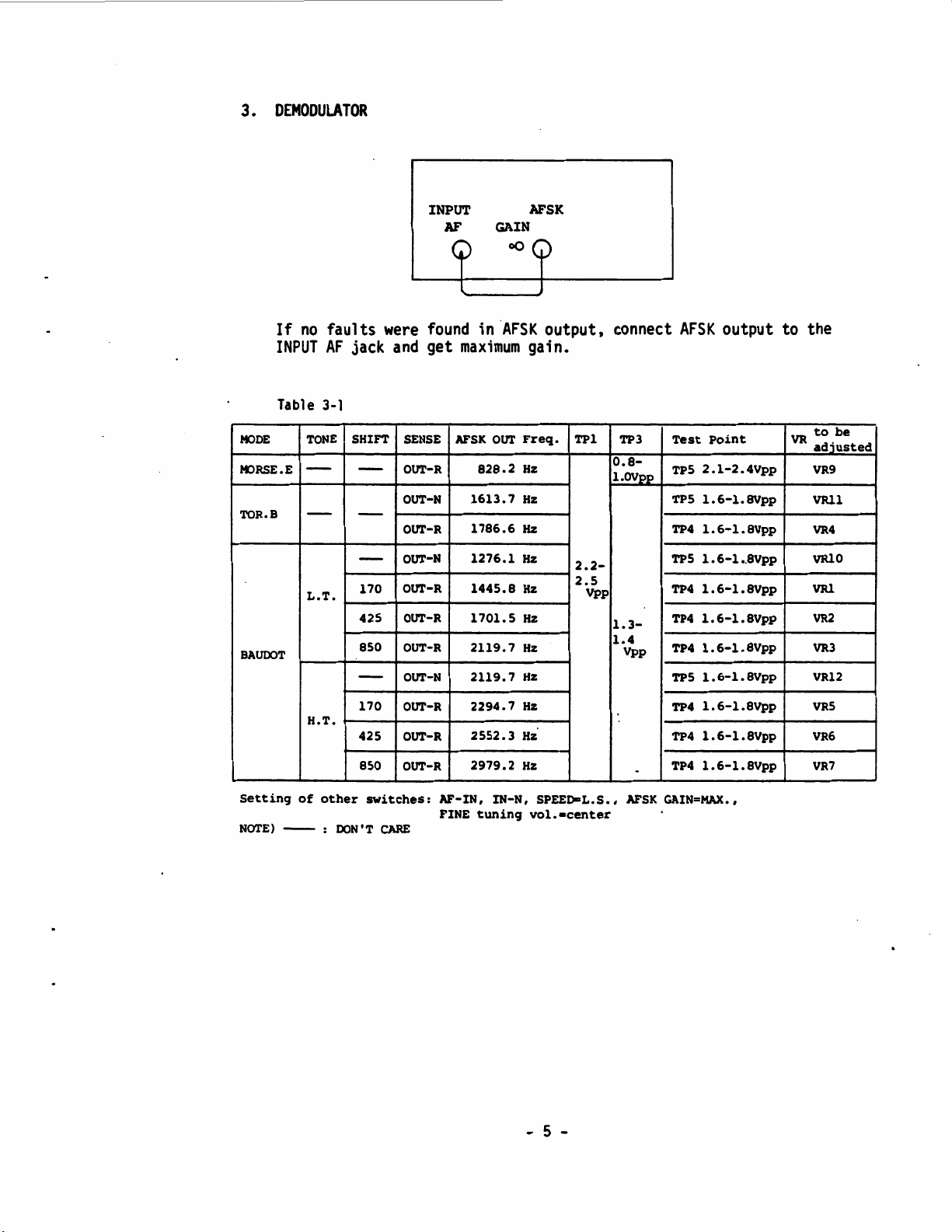
DEMODULATOR
INPUT
AFSK
AF
GAIN
oO
If
no
faults
were
found
in
·AFSK
output,
connect
AFSK
output to the
INPUT
AF
jack
and
get
maximum
gain.
Table 3-1
MOOE
TONE
SHIFT
SENSE
AFSK
Otrl'
Freq.
TPl
TP3
Test
Point
MORSE.E
--Otrr-R
828.2
Hz
o.8-
TP5
2.l-2.4Vpp
1.ov00
OUT-N
1613.7
Hz
TP5
1.6-1.SVpp
TOR.B
--Otrr-R
1786.6
Hz
TP4
1.
6-1.
8Vpp
-
OUT-N
1276.l
Hz
2.2-
TP5
l.6-l
•.
8Vpp
170 Otrr-R
1445.8
Hz
2.5
TP4
1.
6-1.
8Vpp
L.T.
Vpp
425 Otrl'-R
1701.5
Hz
1.3-
TP4
l.6-l.8Vpp
850
OUT-R
2119.7
Hz
1.4
TP4
l.6-l.8Vpp
BAUOOT
Vpp
-Otrr-N 2119.7
Hz
TP5
l.6-l.8Vpp
170 Otrr-R
2294.7
Hz
TP4
l.6-l.8Vpp
H.T. 425
OUT-R
2552.3
Hz·
TP4
l.6-l.8Vpp
850
OUT-R
2979.2
Hz
.
TP4
l.6-l.8Vpp
Setting
of
other
switches:
AF-IN, IN-N, SPEEO-L.S.,
AFSK
GAIN=MAX.,
FINE
tuning
vol.•center
NOTE)
--
:
DON'T
CARE
- 5 -
VR
to
be
adiusted
VR9
VRll
VR4
VRlO
VRl
VR2
VRJ
VR12
VR5
VR6
VR7

3.1
AGC
Circuit·
The
First
Stage of
Band
Pass
Filter
NOISE
FILTER
LPF
for
CW
IC15,
324 TP2
.>----
LPF
___
IC28
1----j,__..-
IC38,
IC39
TRl,
TR2
for
L,'£ 14052
IC15,
324
ANALOG
MULTIPLEXER
S4-9a~--
CW
GAIN
CONTROL
Change
MODE,
TONE,
SHIFT
and
SENSE
as
shown
in
Table
3-1.
Amplitude
of
TPl
and
TP3
should
be
as
shown
in
Table
3-1.
[PROBLEMS]
1.
No
signal or
too
little
signal
is
output
from
TP1.
TP3
,,
,
'\ \
I
,
to
the,'
second
stage
of
B.
P.
F.
___,.
Check
IC38
(3301),
IC39
(3301),
TR1
(2SC536)
and
TR2
(2SC536),
and
check
if
the
circuit
is
disconnected or short-circuit
between
the
AF
IN
jack
and
TPl.
2.
Excessive signal
is
output
from
TPl
..
___.
Check
the
feed
back
circuit
between
R6
and
ca.
3.
No
signal or
too
little
signal
is
output
from
TP3
regardless of
MODE,
TONE,
SHIFT
and
SENSE.
---..
Check
IC28
(14052)
if
no
signal
is
output into
TP2.
Check
IC27
(324)
if
any
signal
is
output into
TP2.
4.
No
signal or
too
little
signal
is
output
from
TP3
in
a certain
state
of
MODE,
TONE,
SHIFT
and
SENSE.
____.
Check
IC15
(324),
IC8
(324)
and
IC28
(14052).
- 6 -
3.2
Adjustment
of the
second
stage of
Band
Pass
Filter
from
LIMITER
AMP.
TP4fH
'I
IC38(3301),
IC32{14066)
-
SPACE
FILTER
I
IC42(14051)
VRl
-~
xl
~-
,
VR2
:J!
x2
7
VR3
~
x3
-, -
VR4
h
x4
~
VR5
7
x5
VR6
-~
x6
J:.
VR7
,
x7
t
VR8
FINE
TUNING
IC39(3301),
IC33(14066)
-
MARK
FILTER
. -
IC43(14052)
_i,.
VR9
~
xO
·
VRlO
xl
, -
VRll
..'I--
x2
,
VR12
_h,.
x3
-I
--
TPS
C)---j
~
,,
to
Detection Circuit
- 7 -
-
VR13
IC48(LB1405)
II
..
I
HSPACE
►
BAR
GRAPH
7.7
H.S./
L.
S./
CW
Control
'
Filter
Switching
Control
.
VR14
IC49(LB1405)
·~
I
MARK
BAR
GRAPH

Table
3-2
Truth
Value
Table
of
Filter
Switching Circuit
MODE
TONE
SHIFT
A(IC21,
B(
IC21,
C(IC6,
a(IC13, b(IC6,
pin3)
pinll) pinll)
pin
11
) pin
11
)
MORSE.E
--0 0 0 0 0
MORSE.J
BAUDOT/TOR.C
L.T.
170 1 0 0 1 0
ASCII/JIS
II
L.T.
425
0 1 0 1 0
II
L.T.
850
1 1 0 1 0
TOR.A
- - 0 0 1 0 1
TOR.B
BAUDOT/TOR.C
L.T.
170
1 0 1 1 1
ASCII/JIS
II
L.T.
425
0 1 1 1 1
II
L.T.
850
1 1 1 1 1
NOTE:
0:
Low
Level
1:
High
Level
Change
MODE,
TONE,
SHIFT
and
SENSE
as
shown
in
Table
3-1
and
adjust cor-
responding trinmer potentiometer to get
maximum
output
from
TP4
and
TPS.
Maximum
amplitude
should
be
l.6Vpp
through
1.8Vpp~
[PROBLEMS]
1.
No
normal
signal
is
output in spite
normal
signal
is
sent to
SPACE
filter,
or the situation
is
incapable of adjustment;
~
1)
Check
IC38
(3301),
IC42
(14051),
IC32
(14066),
YRS
(FINE),
the
trimmer
potentiometer corresponding to
MODE,
TONE
and
SHIFT
which
outputs
no
signal,
and
poor
connection of
CN2.
2)
Check
if
the output of
11
A
11
,
11
8
11
and
11
C
11
in the
filter
switching
circuit
is
corresponding to the
Truth
Value
Table.
NO
Check
IC21
(LS08),
IC6
(LSOO),
IC19
(LS04),
IC13
(LS32),
MODE
switch,
TONE
switch,
SHIFT
switch
and
CN2.
- 8 -

2.
No
normal
signal
is
output in
spite
normal
signal
is
sent to
MARK
filter,
or the situation
is
incapable of adjustment.
~
1)
Check
IC39
(3301),
IC43
(14052),
IC33
(14066)
and
the trilllller
potentiometer corresponding to
MODE
and
TONE
which
output
no
. signal.
2)
Check
if
the output of
"a"
and
"b"
in the
filter
switching
circuit
is
corresponding to the
Truth
Value
Table.
NO
Check
IC21
(LS08),
IC6
(LSOO),
IC19
(LS04),
IC13
(LS32),
MODE
switch,
TONE
switch,
SHIFT
switch
and
CN2.
3.3
Adjustment
of
BAR
GRAPH
SPACE
indicating
BAR
GRAPH
Set the unit in the following
state:
MODE=BAUDOT,
TONE=L.T.,
SHIFT
SHIFT=l70,
OUT-R,
SPEED=L.S.,
AF-IN,
IN-N,
AFSK
GAIN=MAX.,
FINE
TUNING
VOLUME=center.
Turn
VR13
to
minimum,
then turn
it
clockwise gradually
till
the
fifth
LED
lights.
MARK
indicating
BAR
GRAPH
Set the unit in the following
state:
MODE=BAUDOT,
TONE=L.T.,
OUT-N,
SPEED=L.S.,
AF-IN,
IN-N,
AFSK
GAIN=MAX.
Turn
VR14
to
minimum,
then turn
it
clockwise gradually
till
the
fifth
LED
lights.
[PROBLEM]_
1.
LED
does
not
light
to
maximum
for
all
proper signal
is
output
to
TP4
and
TPS.
Check
VR13,
VR14,
IC48
(LB1405),
IC49
(LB1405)
and
CN2.
3.4 Detection Circuit
from
MARK
Filter
from
SPACE
Filter
IC8(324)
Detector
Fig.
3-3
TP
6
IC8(324)
Low
Pass
Filter
- 9 -
TP
7
IC22(339)
TPB
Comparator
ATC/FTL
Control
TPS
(MARK)
TP6
TP7
TPS
1.8V
approx.
1.8V
approx.
---------+-----+----~~----+-----GND
M
s
l.BV
approx.
------~--L.----+------4----~-._
__
GND
s
M------
s
Fig. 3-4.
less
than
0.4V
l.SV
approx.
3.6V
approx.
Set the unit in the following
state:
MODE=BAUDOT,
TONE=L.T.,
SHIFT=l70,
SPEEO=L.S.,
THRESHOLD=ATC.
Transmit
"RY"
test
message
repeatedly
at
50
BPS
by
pressing
11
REPT
11 11
Y
11
•
Make
sure
that
amplitude of
TP6
through
TPS
is
as
shown
in Fig. 3-4.
Make
sure that the
waveform
of
TP6
through
YPS
does
not
change
even
when
the
THRESHOLD
control
is
changed
to
FTL.
Make
sure that the
waveform
remains
in
normal
when
the
state
is
changed
to:
SPEEO=H.S.,
THRESHOLO=ATC,
Baud
Rate=200
BPS.
[PROBLEMS]
1.
The
waveform
of
TP6
is
not
normal.~
Check
017
through
022
and
ICB
(324).
2.
The
waveform
of
TP7
is
not
normal.~
Check
IC7
(14066)
and
ICB
(324).
3.
The
waveform
of
TP8
is
not
normal.~
Check
023, 024,
025,
IC7
(14066)
and
IC22
(324).
-
10
-
4.
The
waveform
does
not
remain
in
~
Check
IC7
(14066),
IC14
(LS02),
normal
when
the
speed
setting
is·
CN2,
SS-6a,
IC32
(14066)
and
changed
to
200
BPS.
IC33
(14066).
NOTE:
It
is
reconmended
to
compare
the
waveform
with
normal
one
by
using
two-channel
oscilloscope, for
it
is
very
difficult
to judge singly
·
whether
the
waveform
is
nonnal
or not.
3.5
ANTI-NOISE
Switching,
AF-TTL
Switching, Input Polarity Switching
Circuit
IC22(339),
IC14(LS02)
from
AGC
from
MARK
filter----..it
from
SPACE
filter
from
MARK=L
DECODE
SPACE=H
S4-9a
cw
TTL
INPUT
JACK~-----'
ANTI-NOISE
GATE
ANTI-NOISE
CONTROL
SS-4a
~SS-la
b
TTL-IN
ICS
LS51
=-'
CPU
Fig.
3-5
cw
!
Otnet·
L
Codes
Level
of
TP9
IN-N
1 ·
IN-R
MARK
=L
SPACE=H
MARK
=H
SPACE=L
-
11
-
H
L
L
H
The
ANTI-NOISE
circuit
works
in the
state
of
A.N.=ON
to
open
the
GATE
when
the input signal
from
MARK
FILTER
or
SPACE
FILTER
is
larger
than
the
one
from
AGC.
Set the unit
as
follows:
MODE=BAUDOT,
SPEED
=L.S.,
TONE=L.T.,
SHIFT=850,
A.N.=ON,
AF-IN.
Make
connection
between
INPUT
AF
and
the variable
audio
generator.
Increase the frequency of the
audio
generator
from
around
800
Hz
to
make
sure that the 1
pin
level of
IC22
(339)
decreases
from
approx.
SV
to
OV
when
the output level of
TPS
becomes
1.1
-
1.2V.
Increase the frequency furthermore to
make
sure
that
the output level
of
TPS
becomes
1.0 -1.lV
when
the frequency
becomes
higher
than
1275
Hz
and
that the 1 pin level of
IC22
increases
from
OV
to
approx.
sv.
Make
sure that
if
the
state
is
changed
to
A.N.=OFF
when
the 1
pin
level of
IC22
is
approx.
5V,
the level decreases to
OV.
The
TP9
level corresponding to
MARK
and
SPACE
is
as
shown
in
Fig. 3-5.
[PROBLEMS]
1.
ANTI
NOISE
circuit
does
not
open.
Check
IC22
(339),
IC14
(LS02)
and
IC21
(LS08).
2.
ANTI
NOISE
circuit
is
left
opened.
Check
IC22
(339),
IC14
(LS02)
and
S5-4a.
3.
The
polarity of the input signal
does
not reverse.
Check
IC26
(LS86),
S5-2a
and
CN2.
-
12
-
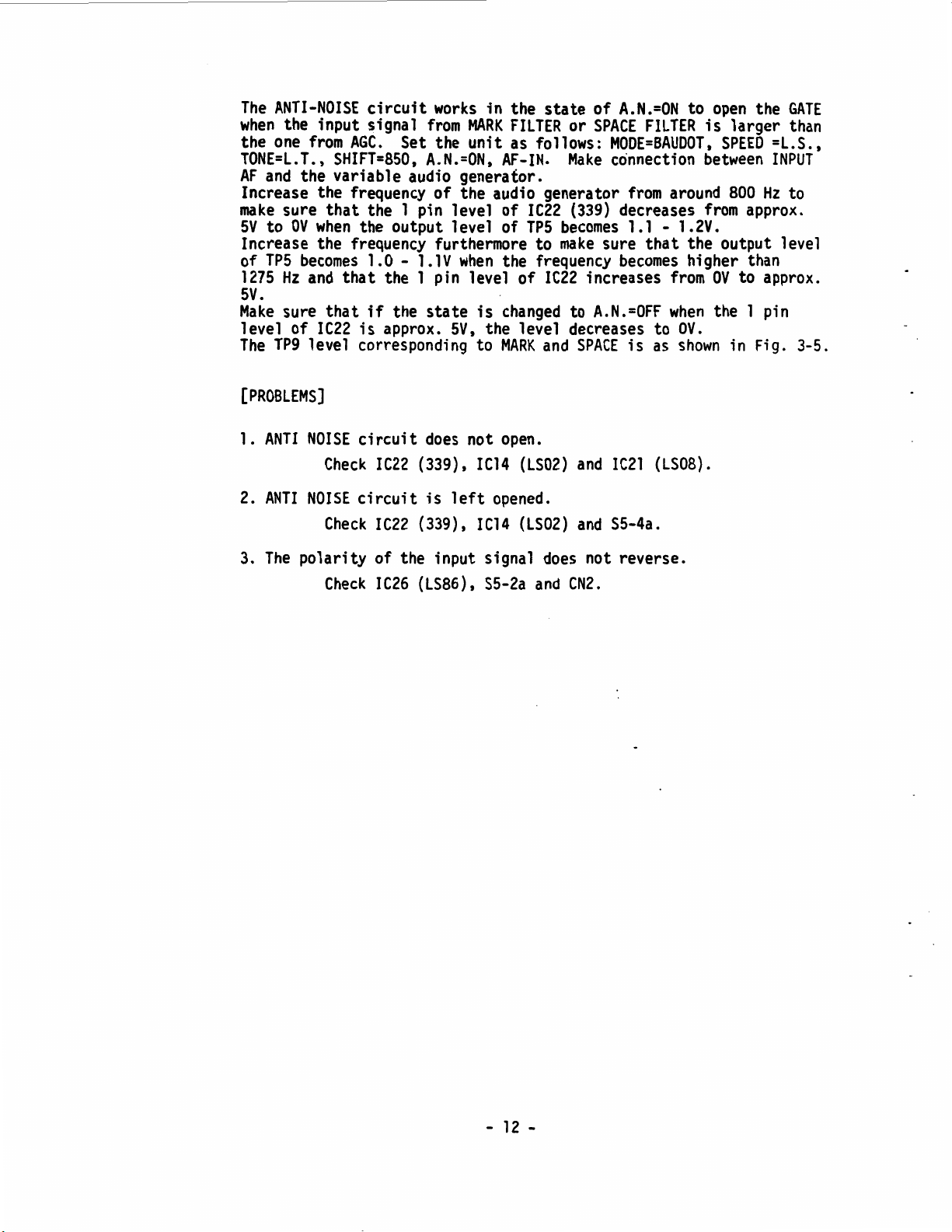
4.
AUCIO
MONITOR
CIRCUIT
PB6
BELL
------------------.---
Cont~
ol
Receiving
signal
IC49(14051
)
AGC
xOANALO
SPACE----4----1xlMULTI
MARK
x2PLEXE
x3
Transmit
~-x4
ting
xS
signal
x6
from---x1
ICll
X
S4-2a
(SPACE)
S4-3a
(MARK)
------P13
TX/RX
Switching
to
.,_~Counter
CN3
to
~~---:!
►
Speaker
The
input signal
sound
being
monitored
is
switched
by
S4-2a
and
S4-3a.
The
input/output signal
sound
is
switched
by
Pl3.
It
is
controlled
by
PB6
to
inject
the bell
sound
into the audio monitor
circuit.
[PROBLEMS]
1.
No
sound
or
too
small
sound
is
heard.
--..check
ICSO
(BA546),
VR16,
the speake~, JS,
CN9
and
Sld.
2.
Only
a certain
sound
is
heard.
---..
Check
I
C49
(
14051
),
CN2,
S4-2a
and
S4-3.a.
3.
No
bell
sound
is
heard.
~
Check
IC22
(339)
and
!Cl
(LSOS).
-
13
-
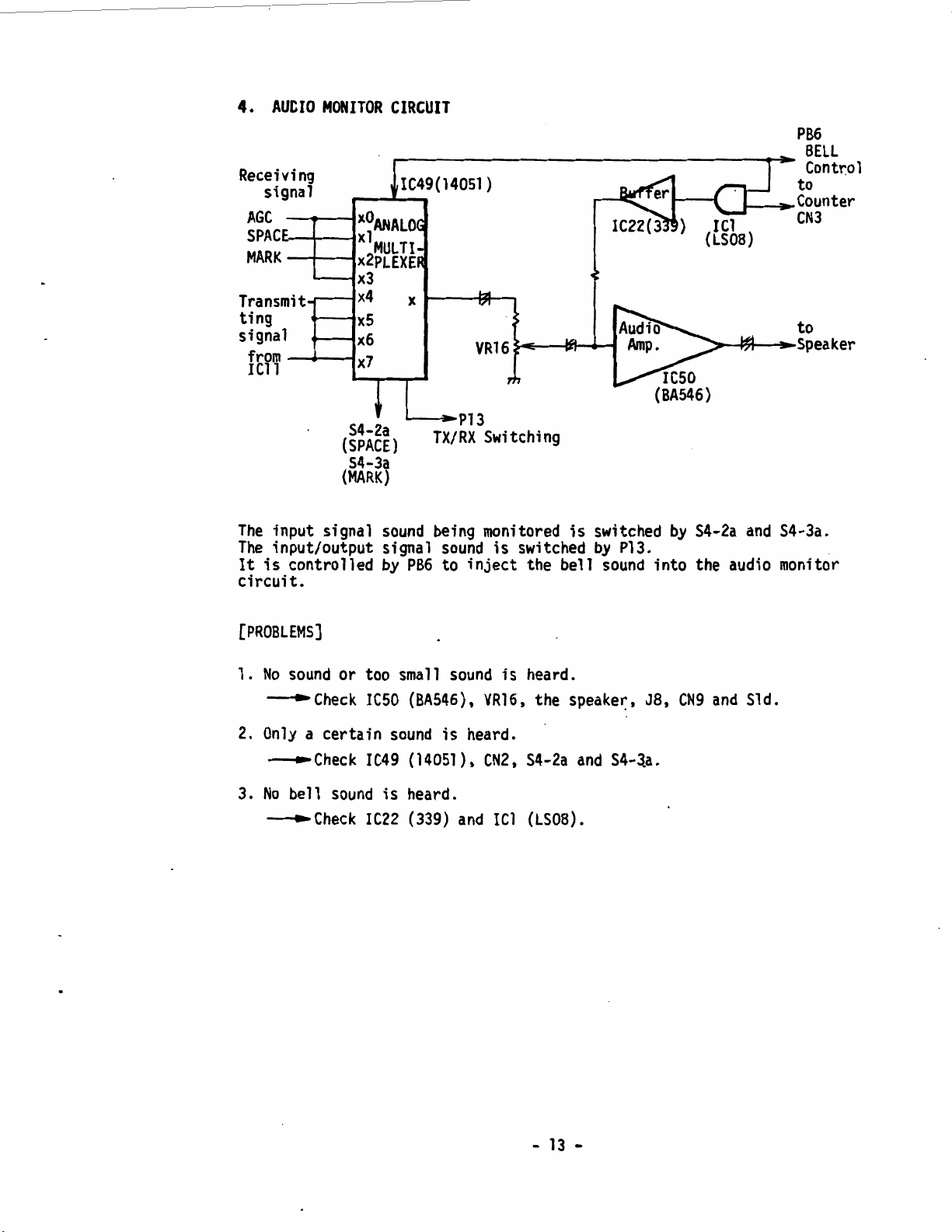
5.
RE5ET,
BATTERY-BACK-UP
CIRCUIT
Rl78.
D2
TR3
Rl84
RST
(to
the
RESET
terminal
Rl87
D5
D4
to
6116VDD
5832VDD
Rlgo T
batteries,
TT7
l.SV
x 2
to
6116
--
CS,
OE
of
8031
and
8255) Fig.
5-1
POWER
SW
ON
RESET
SW
ON
POWER
SW
OFF
i
__
j
___
_
i
+5VDC
POWER
SUPPLY
VOLTAGE
RST
OUTPUT
I
!
i
I
I
!
6116,
5832
Vu
VOLTAGE
6116
VOLTAGE
of
cs,
oo
approx.
4V
<
RESET
CPO
state
activated
I
I
5V
battery
voltage
!
-----5\1
I
□
-~:
)
~
(
)<
)
FSE~
CPU
RESET
I
at~
activated•
state
'
!
I
I
battery
voltage
atter
oltag
----"'~
..
____
....
L-----
Fig.
5-2
-
14
-
fts
~~0w"
in Fig. 5-2,
when
the
RESET
switch
is
pressed
or
when
POWER
ON/
OFF,
the
reset
circuit
generates a
reset
pulse
and
the battery-back-up
circuit
switches the
Vdd
of
IC31
(6116)
and
IC46
(5832)
between
the
+5VOC
main
power
suppll._and
batteries,
and
at
the
same
time
9enerates
hi9h
level
voltage against
r.s
and
OE
of
IC31
(6116)
in order not to
be
chip-selected.
[PROBLEMS]
1.
When
power
is
turned on,
no
reset
function
is
activated
and
CPU
runs
away.
The
capacity of
Cl16
may
be
deficient,
IC22
(339)
may
be
defective,
check
02,
03
and
012.
2.
When
power
is
turned on, the
reset
function
is
activated properly, but
no
reset
function
is
activated
when
the
RESET
button
is
pressed.
t
Check
from
S9-5a
(RESET
button) to
Rl84
through
CN2.
3.
Memorized
date
is
cleared.
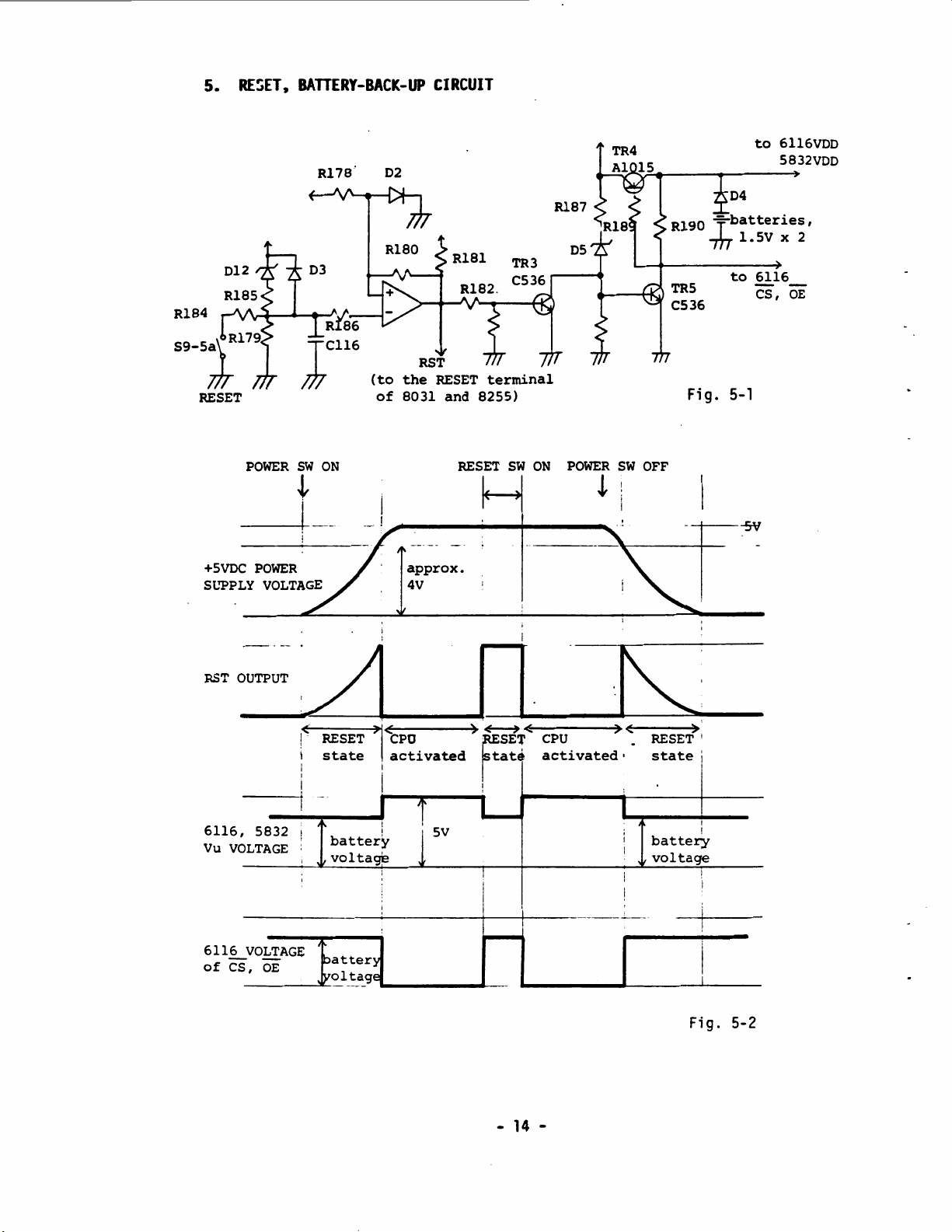
6.
FULL
KEYBOARD
key
matrix
! I
IC4
(14068)
_r-
'--
!
i
!
~7
~
z s
l
~
z
~
~
z
~
z
sz
I I
I
Cl
Ql
Q2
QB
(14094)
5HIFT/STORE
REGISTER
CLK
DATA
STR
i
Check
the battery voltage,
check
TR3,
TR4,
TR5,
04
and
05.
IC2
(
14021)
.
PB
QB
PS
CLK
Pl
P/S
SHIFT
REGISTER
-
15
-
+5VOC
VDO
~VEX
IC3
(14007)
..
multi- C
-
~p
, plexer -
-
30(RXD)
Q
7P
._
31
(TXO)
~
E
...
o
-._ ,
F
-p
._
,
G
11
(KBSTR)
33(INT1)
ND
r
Fig. 6
-1
--

key
matrix
F [
P33
(INTl
)]
E [ Pll
(KBSTR)]
D [
P3l
(TXD)]
C [
P30
(RXD)]
key
pressed-down
1'-----------~I
7
·------~
3 4 5 6 7 8
writino-in
state
to ICl-
l 2 3 4 5 6
rea~ing-in
state
from
IC2
Fig. 6-2 Full
Keyboard
Timing
.
(The
detecting timin9
when
the 0
marked
key
in Fi9. 6-l
is
pressed
down.)
When
the
keys
are not pressed
down,
every output
from
ICl
is
set
to L level
and
the
full
keyboard
is
stopping
its
keyboard scan.
Any
keystroke
is
detected
by
IC4
(14068)
and
starts
the keyboard scan.
-Pll
(KBSTR)
is
set
to H level
to
enable
prograrrming
in
!Cl
(14094).
-
The
data
which
is
to
be
programmed
in
QB
is
set
to
P30.
-
One
clock pulse
is
generated
from
P3l
and
IC2
is
shifted.
-
The
same
procedure
is
repeated
eight
times as
shown
in the figure to
set
date to
Ql-QB.
·
-Pll
is
set
to L level to enable reading-out
from
IC2
(14021).
-
The
data sent to
QB
with
CPU.
-
One
clock pulse
is
generated
from
P31
and
IC2
is
shifted.
-
The
next data
is
output to
QB.
-
The
same
procedure
is
repeated eight times
to
read every data
from
Pl-PB
with
CPU.
-
16
-

[PROBLEMS]
1.
No
keying
acc_epted
1)
The
keyboard
cable
may
be
disconnected or
check
if
CN6.
is
defective
of
contact.
..
2)
Check
ICl
(14094),
IC2
(14021),
IC3
(14007)
and
IC4
(14068)
on
the
keyboard
PCB.
3)
Check
P30,
P31,
P33
and
Pll
of
the
CPU
(8031),
and
also
IC19
(LS04).
2.
The
keying
of
a specified
group
of
keys
is
not accepted.
♦
Check
ICl
(14094),
IC2
(14021),
D1-D8,
IC4
(14068)
and
R9.
3.
The
keying
of
a specified
key
is
not accepted.
♦
The
key-switch
may
be
defective.
7.
SYSTEM
CLOCK
OSCILLATION
CIRCUIT
·
iC3
8.004MHz
_i-F>--
_
___.,.
□---
TP13
IC47(LS04)
IC47(LS04)
IC47
After
warming
up
the
unit,
the output frequency of
TP13
should stay within
8004.000KHz
+/-
O.OSOKHz.
If
not, adjust
TC3
to
make
it
stay within the
range.
[PROBLEMS]
1.
Frequency
error
------4~
2.
No
oscillation-
Re-adjust with
TC3.
Check
IC47
(LS04), crystal
oscillator
and
trinmer capacitor
TC3.
-
17
-
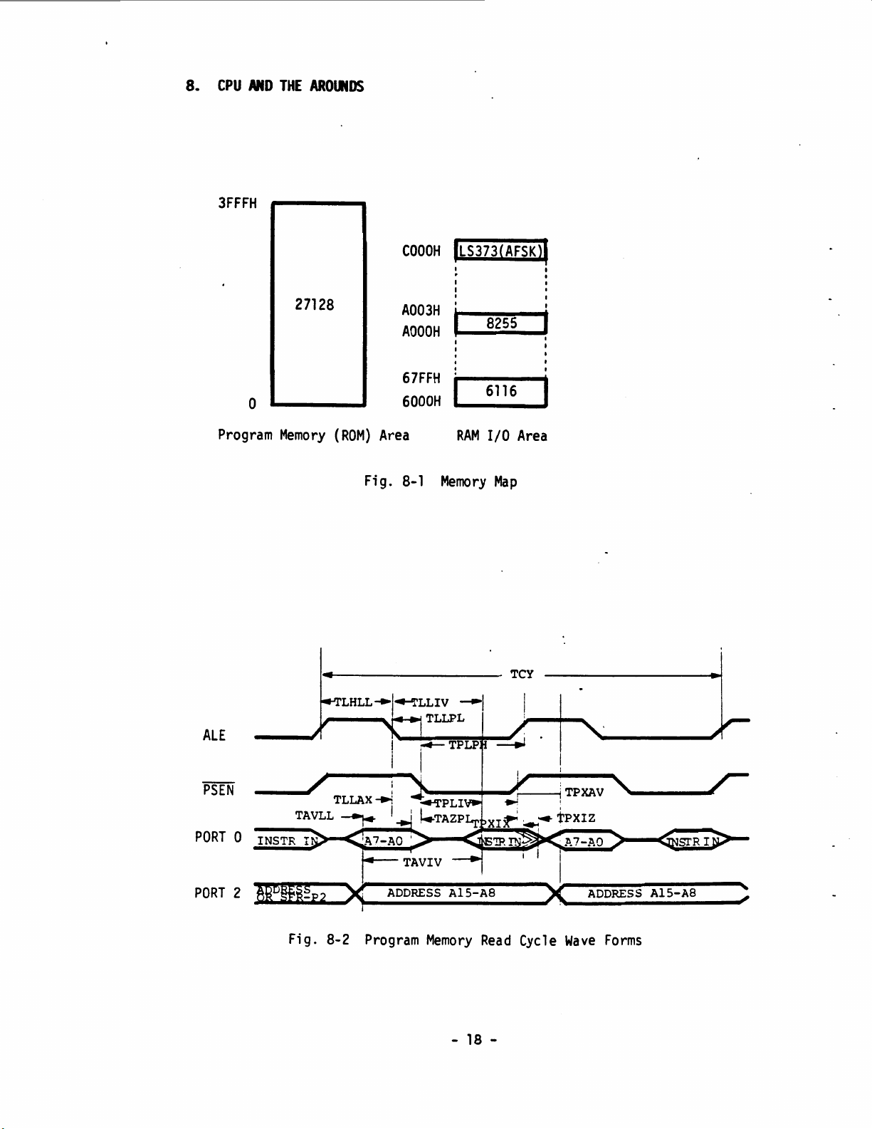
8.
CPU
MD
THE
AROlltDS
3FFFH
COOOH
ILS37
3t
AFSK
ll
~
I
.
.
.
27128
I
A003H
. I
AOOOH
I
8255
I
I
I
I
.
I
67FFH
. I
6000H
I
6116
0
Program
Memory
(ROM)
Area
RAM
1/0
Area
Fig.
8-1
Memory
Map
,.,_
________
TCY
LHLL~,4-'!'LLIV
_.,
TLLPL
ALE
TLLAX
TA
PORT
2
6Q
0
fffi~P2
~,.·
_A_o_o_RE_s_s_A_1s_-_A_s
__
___
: TPXAV
I
I
ADDRESS
Al5-A8
Fig.
8-2
Program
Memory
Read
Cycle
Wave
Forms
-
18
-
Table of contents
Popular Touch Terminal manuals by other brands

QEI
QEI ePAQ-9150 user manual

ZK Technology
ZK Technology iFace 302 Series user guide

Micros Systems
Micros Systems Workstation 4 Setup guide

Vectron
Vectron POS MobilePro III Notes on installation and operation

Festo
Festo CPX-FB38 Electronic manual

Protech Systems
Protech Systems PA-3570 Quick reference guide


