Trenz Electronic TE0808 TRM User manual


TE0808 TRM
Revision: v.32
Copyright © 2019Trenz Electronic GmbH
2 of 46
http://www.trenz-electronic.de
1 Table of Contents
1 Table of Contents................................................................................................................................................... 2
2 Table of Figures...................................................................................................................................................... 4
3 Table of Tables....................................................................................................................................................... 5
4 Overview................................................................................................................................................................. 6
4.1 Key Features........................................................................................................................................................... 6
4.2 Block Diagram ........................................................................................................................................................ 7
4.3 Main Components.................................................................................................................................................. 8
4.4 Initial Delivery State............................................................................................................................................... 9
5 Signals, Interfaces and Pins................................................................................................................................. 10
5.1 Board to Board (B2B) connectors ....................................................................................................................... 10
5.2 MGT Lanes ............................................................................................................................................................ 12
5.3 JTAG Interface...................................................................................................................................................... 17
5.4 Configuration Bank Control Signals.................................................................................................................... 18
5.5 Analog Input ......................................................................................................................................................... 18
5.6 Quad SPI Interface ............................................................................................................................................... 19
6 Boot Process......................................................................................................................................................... 20
7 On-board Peripherals .......................................................................................................................................... 22
7.1 Flash...................................................................................................................................................................... 22
7.2 DDR4 SDRAM ........................................................................................................................................................ 22
7.3 Programmable PLL Clock Generator .................................................................................................................. 22
7.4 Oscillators............................................................................................................................................................. 24
7.5 On-board LEDs ..................................................................................................................................................... 24
8 Power and Power-On Sequence ......................................................................................................................... 25
8.1 Power Consumption ............................................................................................................................................ 25
8.2 Power Distribution Dependencies ...................................................................................................................... 26
8.3 Power-On Sequence Diagram ............................................................................................................................. 28
8.4 Operation Conditions of the DC-DC Converter Control Signals ........................................................................ 29
8.5 Voltage Monitor Circuit........................................................................................................................................ 32
8.6 Power Rails........................................................................................................................................................... 32
8.7 Bank Voltages....................................................................................................................................................... 33
9 B2B connectors .................................................................................................................................................... 35
9.1 Features................................................................................................................................................................ 35
9.2 Connector Stacking height.................................................................................................................................. 35
9.3 Current Rating...................................................................................................................................................... 36
9.4 Connector Speed Ratings .................................................................................................................................... 36

TE0808 TRM
Revision: v.32
Copyright © 2019Trenz Electronic GmbH
3 of 46
http://www.trenz-electronic.de
9.5 Manufacturer Documentation............................................................................................................................ 36
10 Variants Currently In Production ........................................................................................................................ 38
11 Technical Specifications...................................................................................................................................... 39
11.1 Absolute Maximum Ratings................................................................................................................................. 39
11.2 Recommended Operating Conditions ................................................................................................................ 40
11.3 Operating Temperature Ranges.......................................................................................................................... 41
11.4 Physical Dimensions ............................................................................................................................................ 41
12 Revision History ................................................................................................................................................... 43
12.1 Hardware Revision History.................................................................................................................................. 43
12.2 Document Change History .................................................................................................................................. 43
13 Disclaimer............................................................................................................................................................. 45
13.1 Data privacy ......................................................................................................................................................... 45
13.2 Document Warranty............................................................................................................................................. 45
13.3 Limitation of Liability........................................................................................................................................... 45
13.4 Copyright Notice .................................................................................................................................................. 45
13.5 Technology Licenses............................................................................................................................................ 45
13.6 Environmental Protection ................................................................................................................................... 45
13.7 REACH, RoHS and WEEE ...................................................................................................................................... 45


TE0808 TRM
Revision: v.32
Copyright © 2019Trenz Electronic GmbH
6 of 46
http://www.trenz-electronic.de
4 Overview
The Trenz Electronic TE0808 is an industrial-grade MPSoC SoM integrating a Xilinx Zynq UltraScale+ MPSoC, up to 8
GBytes of DDR4 SDRAM via 64-bit wide data bus, max. 512 MByte Flash memory for configuration and operation, 20
Gigabit transceivers and powerful switch-mode power supplies for all on-board voltages. A large number of
configurable I/Os are provided via rugged high-speed stacking connections. All this in a compact 5.2 x 7.6 cm form
factor, at the competitive price.
Refer to http://trenz.org/te0808-info for the current online version of this manual and other available
documentation.
4.1 Key Features
•MPSoC: ZYNQ UltraScale+ ZU9EG 900 pin package
•Memory
- 64-Bit DDR4, 8 GByte maximum
- Dual SPI boot Flash in parallel, 512 MByte maximum
•User I/Os
- 65 x PS MIOs, 48 x PL HD GPIOs, 156 x PL HP GPIOs (3 banks)
- Serial transceivers: 4 x GTR + 16 x GTH
- Transceiver clocks inputs and outputs
- PLL clock generator inputs and outputs
•Si5345 - 10 output PLL
•All power supplies on board, single 3.3V power source required
- 14 on-board DC-DC regulators and 13 LDOs
- LP, FP, PL separately controlled power domains
•Support for all boot modes (except NAND) and scenarios
•Support for any combination of PS connected peripherals
•Size: 52 x 76 mm, 3 mm mounting holes for skyline heat spreader
•B2B connectors: 4 x 160 pin


TE0808 TRM
Revision: v.32
Copyright © 2019Trenz Electronic GmbH
8 of 46
http://www.trenz-electronic.de
4.3 Main Components
Figure 2: TE0808 MPSoC module.
1. Xilinx ZYNQ UltraScale+ XCZU9EG MPSoC, U1
2. Low-power programmable oscillator @ 33.333333 MHz (PS_CLK), U32
3. Red LED (DONE), D1
4. 256Mx16 DDR4-2400 SDRAM, U12
5. 256Mx16 DDR4-2400 SDRAM, U9
6. 256Mx16 DDR4-2400 SDRAM, U2
7. 256Mx16 DDR4-2400 SDRAM, U3
8. 12A PowerSoC DC-DC converter, U4
9. Quartz crystal, Y1
10. Low-power programmable oscillator @ 25.000000 MHz (IN0 for U5), U25
11. 10-channel programmable PLL clock generator, U5
12. Ultra fine 0.50 mm pitch, Razor Beam™LP Slim Terminal Strip with 160 contacts, J4
13. Ultra fine 0.50 mm pitch, Razor Beam™LP Slim Terminal Strip with 160 contacts, J2
14. Ultra fine 0.50 mm pitch, Razor Beam™LP Slim Terminal Strip with 160 contacts, J3
15. Ultra fine 0.50 mm pitch, Razor Beam™LP Slim Terminal Strip with 160 contacts, J1
16. Quartz crystal, Y2
TE0808 TRM
Revision: v.32
Copyright © 2019Trenz Electronic GmbH
9 of 46
http://www.trenz-electronic.de
17. 256 Mbit serial NOR Flash memory, U7
18. 256 Mbit serial NOR Flash memory, U17
4.4 Initial Delivery State
Storage device name Content Notes
SPI Flash main array Not programmed -
eFUSE Security Not programmed -
Si5345A programmable PLL NVM OTP Not programmed -
Table 1: Initial Delivery State of the flash memories.

TE0808 TRM
Revision: v.32
Copyright © 2019Trenz Electronic GmbH
10 of 46
http://www.trenz-electronic.de
5 Signals, Interfaces and Pins
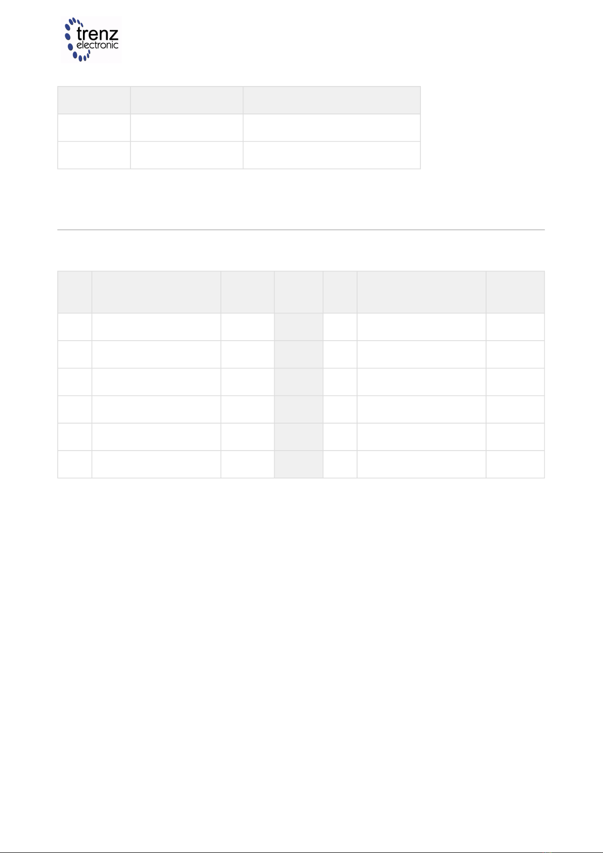
5.1 Board to Board (B2B) connectors
The TE0808 MPSoC SoM has four Board to Board (B2B) connectors with 160 contacts per connector.
Each connector has a specific arrangement of the signal pins, which are grouped together in categories related to
their functionalities and to their belonging to particular units of the Zynq UltraScale+ MPSoC like I/O banks,
interfaces and Gigabit transceivers
or to the on-board peripherals.
Following table lists the I/O-bank signals, which are routed from the MPSoC's PL and PS banks as LVDS pairs or
single ended I/O's to the B2B connectors.
Bank Type B2B
Connecto
r
Schemati
c Names /
Connecto
r Pins
I/O
Signals
LVDS
Pairs
VCCO
Bank
Voltage
Notes
47 HD J3 B47_L1_P
...
B47_L12_
P
B47_L1_N
...
B47_L12_
N
24 I/Os 12 VCCO47
pins
J3-43,
J3-44
VCCO
max. 3.3V
usableas
single-
ended I/
Os
48 HD J3 B48_L1_P
...
B48_L12_
P
B48_L1_N
...
B48_L12_
N
24 I/Os 12 VCCO48
pins
J3-15,
J3-16
VCCO
max. 3.3V
usableas
single-
ended I/
Os

TE0808 TRM
Revision: v.32
Copyright © 2019Trenz Electronic GmbH
11 of 46
http://www.trenz-electronic.de
Bank Type B2B
Connecto
r
Schemati
c Names /
Connecto
r Pins
I/O
Signals
LVDS
Pairs
VCCO
Bank
Voltage
Notes
64 HP J4 B64_L1_P
...
B64_L24_
P
B64_L1_N
...
B64_L24_
N
B_64_T0 ..
. B_64_T3
52 I/O's 24 VCCO64
pins
J4-58,
J4-106
VCCO
max. 1.8V
usable as
single-
ended I/
Os
65 HP J4 B65_L1_P
...
B65_L24_
P
B65_L1_N
...
B65_L24_
N
B_65_T0 ..
. B_65_T3
52 I/Os 24 VCCO65
pins
J4-69,
J4-105
VCCO
max. 1.8V
usableas
single-
ended I/
Os
66 HP J1 B66_L1_P
...
B66_L24_
P
B66_L1_N
...
B66_L24_
N
B_66_T0 ..
. B_66_T3
48 I/Os 24 VCCO66
pins
J1-90,
J1-120
VCCO
max. 1.8V
usableas
single-
ended I/
Os
500 MIO J3 MIO13 ...
MIO25
13 I/Os - PS_1V8 User
configura
ble I/Os
on B2B

TE0808 TRM
Revision: v.32
Copyright © 2019Trenz Electronic GmbH
12 of 46
http://www.trenz-electronic.de
1 https://shop.trenz-electronic.de/de/Download/?path=Trenz_Electronic/Pinout
Bank Type B2B
Connecto
r
Schemati
c Names /
Connecto
r Pins
I/O
Signals
LVDS
Pairs
VCCO
Bank
Voltage
Notes
501 MIO J3 MIO26 ...
MIO51
26 I/Os - PS_1V8 User
configura
ble I/Os
on B2B
502 MIO J3 MIO52 ...
MIO77
26 I/Os - PS_1V8 User
configura
ble I/Os
on B2B
Table 2:B2B connector pin-outs of available PL and PS banks of the TE0808-04 SoM.
All MIO banks are powered from on-module DC-DC power rail. All PL I/O Banks have separate VCCO pins in the B2B
connectors, valid VCCO should be supplied from the baseboard.
For detailed information about the B2B pin-out, please refer to thePin-out1table.
The configuration of the I/O's MIO13 - MIO77 are depending on the base-board peripherals connected to these pins.
5.2 MGT Lanes
The B2B connector J1 and J2 provide also access to the MGT banks of the Zynq UltraScale+ MPSoC. There are 20
high-speed data lanes (Xilinx GTH / GTR transceiver) available composed as differential signaling pairs for both
directions (RX/TX).
The MGT banks have also clock input-pins which are exposed to the B2B connectors J2 and J3. Following MGT lanes
are available on the B2B connectors:

TE0808 TRM
Revision: v.32
Copyright © 2019Trenz Electronic GmbH
13 of 46
http://www.trenz-electronic.de
Bank Type B2B
Connector
Count of MGT
Lanes
Schematic
Names /
Connector Pins
MGT Bank's
Reference Clock
Inputs
228 GTH J1 4 GTH lanes
(4 RX / 4 TX)
B228_RX3_P,
B228_RX3_N, pins
J1-51, J1-53
B228_TX3_P,
B228_TX3_N, pins
J1-50, J1-52
B228_RX2_P,
B228_RX2_N, pins
J1-57, J1-59
B228_TX2_P,
B228_TX2_N, pins
J1-56, J1-58
B228_RX1_P,
B228_RX1_N, pins
J1-63, J1-65
B228_TX1_P,
B228_TX1_N, pins
J1-62, J1-63
B228_RX0_P,
B228_RX0_N, pins
J1-69, J1-71
B228_TX0_P,
B228_TX0_N, pins
J1-68, J1-70
1 reference clock
signal
(B228_CLK0) from
B2B connector
J3 (pins J3-60,
J3-62) to bank's
pins R8/R7
1 reference clock
signal
(B228_CLK1) from
programmable
PLL clock
generator U5 to
bank's pins N8/N7

TE0808 TRM
Revision: v.32
Copyright © 2019Trenz Electronic GmbH
14 of 46
http://www.trenz-electronic.de
Bank Type B2B
Connector
Count of MGT
Lanes
Schematic
Names /
Connector Pins
MGT Bank's
Reference Clock
Inputs
229 GTH J1 4 GTH lanes
(4 RX / 4 TX)
B229_RX3_P,
B229_RX3_N, pins
J1-27, J1-29
B229_TX3_P,
B229_TX3_N, pins
J1-26, J1-28
B229_RX2_P,
B229_RX2_N, pins
J1-33, J1-35
B229_TX2_P,
B229_TX2_N, pins
J1-32, J1-34
B229_RX1_P,
B229_RX1_N, pins
J1-39, J1-41
B229_TX1_P,
B229_TX1_N, pins
J1-38, J1-40
B229_RX0_P,
B229_RX0_N, pins
J1-45, J1-47
B229_TX0_P,
B229_TX0_N, pins
J1-44, J1-46
1 reference clock
signal
(B229_CLK0) from
B2B connector
J3 (pins J3-65,
J3-67) to bank's
pins L8/L7
1 reference clock
signal
(B229_CLK1) from
programmable
PLL clock
generator U5 to
bank's pins J8/J7

TE0808 TRM
Revision: v.32
Copyright © 2019Trenz Electronic GmbH
15 of 46
http://www.trenz-electronic.de
Bank Type B2B
Connector
Count of MGT
Lanes
Schematic
Names /
Connector Pins
MGT Bank's
Reference Clock
Inputs
230 GTH J1 4 GTH lanes
(4 RX / 4 TX)
B230_RX3_P,
B230_RX3_N, pins
J1-3, J1-5
B230_TX3_P,
B230_TX3_N, pins
J1-2, J1-4
B230_RX2_P,
B230_RX2_N, pins
J1-9, J1-11
B230_TX2_P,
B230_TX2_N, pins
J1-8, J1-10
B230_RX1_P,
B230_RX1_N, pins
J1-15, J1-17
B230_TX1_P,
B230_TX1_N, pins
J1-14, J1-16
B230_RX0_P,
B230_RX0_N, pins
J1-21, J1-23
B230_TX0_P,
B230_TX0_N, pins
J1-20, J1-22
1 reference clock
signal
(B230_CLK1) from
B2B connector
J3 (pins J3-59,
J3-61) to bank's
pins G8/G7
1 reference clock
signal
(B230_CLK0) from
programmable
PLL clock
generator U5 to
bank's pins E8/E7

TE0808 TRM
Revision: v.32
Copyright © 2019Trenz Electronic GmbH
16 of 46
http://www.trenz-electronic.de
Bank Type B2B
Connector
Count of MGT
Lanes
Schematic
Names /
Connector Pins
MGT Bank's
Reference Clock
Inputs
128 GTH J2 4 GTH lanes
(4 RX / 4 TX)
B128_RX3_N,
B128_RX3_P, pins
J2-28, J2-30
B128_TX3_N,
B128_TX3_P, pins
J2-25, J2-27
B128_RX2_N,
B128_RX2_P, pins
J2-34, J2-36
B128_TX2_N,
B128_TX2_P, pins
J2-31, J2-33
B128_RX1_N,
B128_RX1_P, pins
J2-40, J2-42
B128_TX1_N,
B128_TX1_P, pins
J2-37, J2-39
B128_RX0_N,
B128_RX0_P, pins
J2-46, J2-48
B128_TX0_N,
B128_TX0_P, pins
J2-43, J2-45
1 reference clock
signal
(B128_CLK1) from
B2B connector
J2 (pins J2-22,
J2-24) to bank's
pins D25/D26
1 reference clock
signal
(B128_CLK0) from
programmable
PLL clock
generator U5 to
bank's pins F25/
F26

TE0808 TRM
Revision: v.32
Copyright © 2019Trenz Electronic GmbH
17 of 46
http://www.trenz-electronic.de
Bank Type B2B
Connector
Count of MGT
Lanes
Schematic
Names /
Connector Pins
MGT Bank's
Reference Clock
Inputs
505 GTR J2 4 GTR lanes
(4 RX / 4 TX)
B505_RX3_N,
B505_RX3_P, pins
J2-52, J2-54
B505_TX3_N,
B505_TX3_P, pins
J2-49, J2-51
B505_RX2_N,
B505_RX2_P, pins
J2-58, J2-60
B505_TX2_N,
B505_TX2_P, pins
J2-55, J2-57
B505_RX1_N,
B505_RX1_P, pins
J2-64, J2-66
B505_TX1_N,
B505_TX1_P, pins
J2-61, J2-63
B505_RX0_N,
B505_RX0_P, pins
J2-70, J2-72
B505_TX0_N,
B505_TX0_P, pins
J2-67, J2-69
2 reference clock
signals
(B505_CLK0,
B505_CLK1) from
B2B connector
J2 (pins J2-10/
J2-12, J2-16/
J2-18) to bank's
pins P25/P26,
M25/M26
2 reference clock
signal
(B505_CLK2,
B505_CLK3) from
programmable
PLL clock
generator U5 to
bank's pins K25/
K26, H25/H26
Table 3: B2B connector pin-outs of available MGT lanes of the MPSoC.
5.3 JTAG Interface
JTAG access is provided through the MPSoC's PS configuration bank 503 with bank voltage PS_1V8.
JTAG Signal B2B Connector Pin
TCK J2-120
TDI J2-122
TDO J2-124
TMS J2-126

TE0808 TRM
Revision: v.32
Copyright © 2019Trenz Electronic GmbH
18 of 46
http://www.trenz-electronic.de
2 https://www.xilinx.com/support/documentation/user_guides/ug1085-zynq-ultrascale-trm.pdf
3 https://www.xilinx.com/support/documentation/user_guides/ug570-ultrascale-configuration.pdf
Table 4: B2B connector pin-out of JTAG interface.
5.4 Configuration Bank Control Signals
The Xilinx Zynq UltraScale+ MPSoC's PS configuration bank 503 control signal pins are accessible through B2B
connector J2.
For further information about the particular control signals and how to use and evaluate them, refer to the Xilinx
Zynq UltraScale+ MPSoC TRM2and UltraScale Architecture Configuration - User Guide3.
Signal B2B Connector Pin Function
DONE J2-116 PL configuration completed.
PROG_B J2-100 PL configuration reset signal.
INIT_B J2-98 PS is initialized after a power-on reset.
SRST_B J2-96 System reset.
MODE0 ... MODE3 J2-109/J2-107/J2-105/
J2-103
4-bit boot mode pins.
For further information about the boot
modes refer to the Xilinx Zynq
UltraScale+ MPSoC TRM section 'Boot
and Configuration'.
ERR_STATUS /
ERR_OUT
J2-86 / J2-88 ERR_OUT signal is asserted for
accidental loss of power, an error, or
an exception in the MPSoC's Platform
Management Unit (PMU).
ERR_STATUS indicates a secure lock-
down state.
PUDC_B J2-127 Pull-up during configuration (pulled-up
to PL_1V8).
Table 5: B2B connector pin-out of MPSoC's PS configuration bank.
5.5 Analog Input
The Xilinx Zynq UltraScale+ MPSoC provides differential pairs for analog input values. The pins are exposed to B2B-
connector J2.
TE0808 TRM
Revision: v.32
Copyright © 2019Trenz Electronic GmbH
19 of 46
http://www.trenz-electronic.de
Signal B2B Connector Pin Function
V_P, V_N J2-113, J2-115 System Monitor
DX_P, DX_N J2-119, J2-121 Temperature-sensing diode pins
Table 6: B2B connector pin-out of analog input pins
5.6 Quad SPI Interface
Quad SPI Flash memory ICs U7 and U17 are connected to the Zynq MPSoC PS QSPI0 interface via PS MIO bank 500,
pins MIO0 ... MIO5 and MIO7 ... MIO12.
MI
O
Signal Name U7 Pin MI
O
Signal Name U17 Pin
0 SPI Flash CLK B2 7 SPI Flash CS C2
1 SPI Flash IO1 D2 8 SPI Flash IO0 D3
2 SPI Flash IO2 C4 9 SPI Flash IO1 D2
3 SPI Flash IO3 D4 10 SPI Flash IO2 C4
4 SPI Flash IO0 D3 11 SPI Flash IO3 D4
5 SPI Flash CS C2 12 SPI Flash CLK B2
Table 7: PS MIO pin assignment of the Quad SPI Flash memory ICs.

TE0808 TRM
Revision: v.32
Copyright © 2019Trenz Electronic GmbH
20 of 46
http://www.trenz-electronic.de
6 Boot Process
The boot device and mode of the Zynq UltraScale+ MPSoC can be selected via 4 dedicated pins accessible on B2B
connector J2:
Boot Mode Pin B2B Pin
PS_MODE0 J2-109
PS_MODE1 J2-107
PS_MODE2 J2-105
PS_MODE3 J2-103
Table 8: Boot mode pins on B2B connector J2.
Following boot modes are possible on the TE0808 UltraScale+ module by generating the corresponding 4-bit code
by the pins PS_MODE0 ... PS_MODE3 (little-endian alignment):
Boot
Mode
Mode Pins
[3:0]
MIO
Location
Description
JTAG 0x0 JTAG Dedicated PS interface.
QSPI32 0x2 MIO[12:0] Configured on module with dual QSPI Flash
Memory.
32-bit addressing.
Supports single and dual parallel
configurations.
Stack and dual stack is not
supported.
SD0 0x3 MIO[25:13] Supports SD 2.0.
SD1 0x5 MIO[51:38] Supports SD 2.0.
eMMC_18 0x6 MIO[22:13] Supports eMMC 4.5 at 1.8V.
USB 0 0x7 MIO[52:63] Supports USB 2.0 and USB 3.0.
PJTAG_0 0x8 MIO[29:26] PS JTAG connection 0 option.
SD1-LS 0xE MIO[51:39] Supports SD 3.0 with a required SD 3.0
compliant level shifter.
Table 9: Selectable boot modes by dedicated boot mode pins.
Table of contents
Popular Industrial PC manuals by other brands


Siemens
Siemens Simatic IPC647C operating instructions

Kontron
Kontron KISS 2U V3 user guide

Acorn
Acorn ARM Evaluation System user guide

Emerson
Emerson FB1100 Field Replacement Guide

Chipsee
Chipsee PPC-A72-156-P instruction manual

Digital Electronics Corporation
Digital Electronics Corporation PS-2000B Series installation guide

GIGAIPC
GIGAIPC QBiX-Pro-TGLA1115G4EH-A1 quick start guide

Allen-Bradley
Allen-Bradley 6155R-NSXP installation instructions

BENECOM
BENECOM BNC-122 user guide

FabiaTech
FabiaTech FX5505 Series Users Quick Reference

Aprotech
Aprotech GOLUB 45 Series user manual

ADLINK Technology
ADLINK Technology DLAP-3000 Series user manual