Velleman-Kit K8050 User manual

15 Channel infrared receiver
K8050
ILLUSTRATED ASSEMBLY MANUAL H8050IP-1
Total solder points: 248
Difficulty level: beginner 1 2 3 4 5 advanced
IR-Remotecontroltransmitters
allowyoutocontrol15open-
collectorcontacts

2
Features:
Works together with K6710, K8049, K8051, K8055, K8056, K6714 -(16), K2633, …
15 open collector contacts : Max. 50V/50mA.
LED indication for each output.
Multiple sensors possible.
Transmitter - Receiver range : up to 20m
4 different modes :
• 15 independent outputs.
• 15 rotary outputs
• 7 independent outputs & 8 rotary outputs.
• 7 rotary outputs & 8 rotary outputs (independent from each other).
3 addressed allow the use of multiple receivers in one room.
Optional board-to-wire connectors-female (BTWF5 & BTWF20)
Optional IR-receivers (IR38DM)
Specifications:
Power supply : 8 –14VDC or 2x6 to 2x12VAC (150mA).
Current consumption : all outputs off : 10mA
all outputs on : 150mA
Features & Specifications

3
Assembly hints
1. Assembly (Skipping this can lead to troubles ! )
Ok, so we have your attention. These hints will help you to make this project successful. Read them carefully.
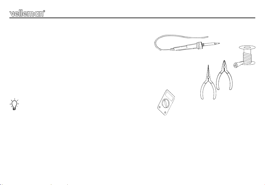
1.1 Make sure you have the right tools:
• A good quality soldering iron (25-40W) with a small tip.
• Wipe it often on a wet sponge or cloth, to keep it clean; then apply solder to the tip, to give it a wet look. This is called ‘thinning’ and will
protect the tip, and enables you to make good connections. When solder rolls off the tip, it needs cleaning.
• Thin raisin-core solder. Do not use any flux or grease.
• A diagonal cutter to trim excess wires. To avoid injury when cutting excess leads, hold the lead so they
cannot fly towards the eyes.
• Needle nose pliers, for bending leads, or to hold components in place.
• Small blade and Phillips screwdrivers. A basic range is fine.
For some projects, a basic multi-meter is required, or might be handy
1.2 Assembly Hints :
⇒ Make sure the skill level matches your experience, to avoid disappointments.
⇒ Follow the instructions carefully. Read and understand the entire step before you perform each operation.
⇒ Perform the assembly in the correct order as stated in this manual
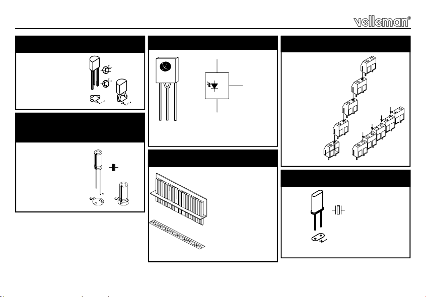
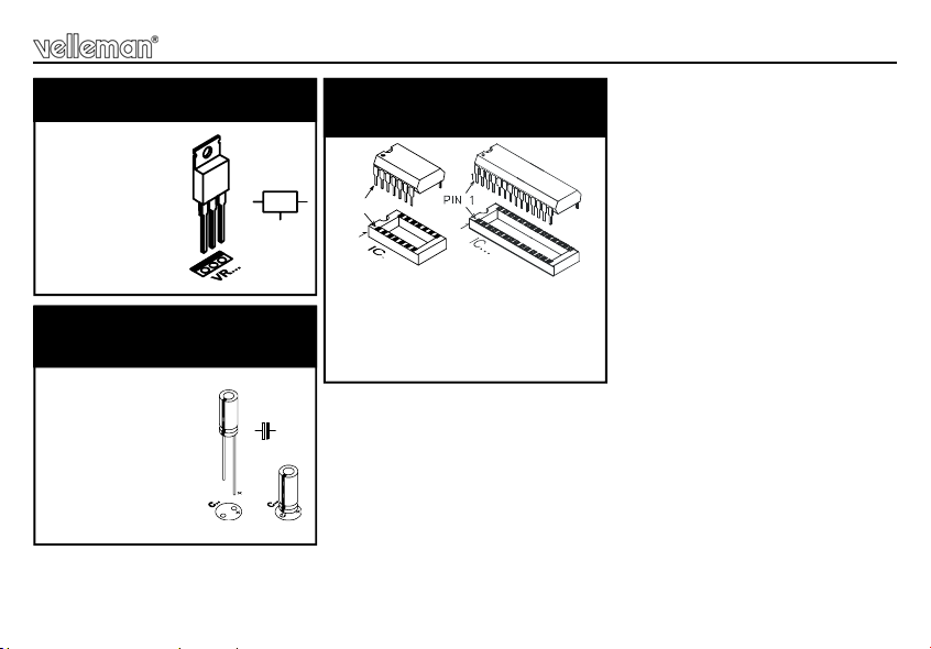
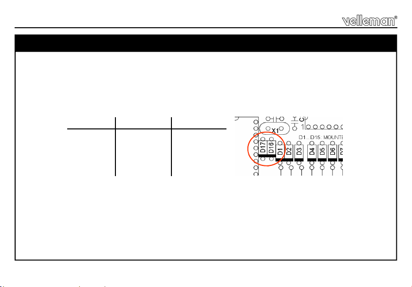
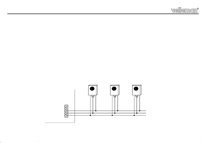
⇒ Position all parts on the PCB (Printed Circuit Board) as shown on the drawings.
⇒ Values on the circuit diagram are subject to changes.
⇒ Values in this assembly guide are correct*
⇒ Use the check-boxes to mark your progress.
⇒ Please read the included information on safety and customer service
* Typographical inaccuracies excluded. Always look for possible last minute manual updates, indicated as ‘NOTE’ on a separate leaflet.
0
.0
0
0

4
Assembly hints
1.3 Soldering Hints :
1- Mount the component against the PCB surface and carefully solder the leads
2- Make sure the solder joints are cone-shaped and shiny
3- Trim excess leads as close as possible to the solder joint
REMOVE THEM FROM THE TAPE ONE AT A TIME !
AXIAL COMPONENTS ARE TAPED IN THE COR-
RECT MOUNTING SEQUENCE !

5
R1 : 390 (3-9-1-B)
R2 : 390 (3-9-1-B)
R3 : 390 (3-9-1-B)
R4 : 390 (3-9-1-B)
R5 : 390 (3-9-1-B)
R6 : 390 (3-9-1-B)
R7 : 390 (3-9-1-B)
2. Resistors
R...
Construction
IC1 : 28p
IC2 : 16p
IC3 : 18p
3. IC’s.
D20 : 1N4007
D21 : 1N4007
Remark: D1 to D19 are not
mounted at this time.
1. Diodes, check the polarity
D...
CATHODE
R8 : 390 (3-9-1-B)
R9 : 390 (3-9-1-B)
R10 : 390 (3-9-1-B)
R11 : 390 (3-9-1-B)
R12 : 390 (3-9-1-B)
R13 : 390 (3-9-1-B)
R14 : 390 (3-9-1-B)
R15 : 390 (3-9-1-B)
R16 : 390 (3-9-1-B)
R17 : 10K (1-0-2-B)
R18 : 10K (1-0-2-B)
R19 : 10K (1-0-2-B)
R20 : 10K (1-0-2-B)
C1 : 18pF (18)
C2 : 18pF (18)
C3 : 100nF (104, u1)
C4 : 100nF (104, u1)
C5 : 100nF (104, u1)
C6 : 100nF (104, u1)
4. Ceramic Capacitors
C...
5. LED’s. Watch the polarity!
3mm Red
LD1
LD2
LD3
LD4
LD5
LD6
LD7
LD8
LD9
LD10
LD11
LD12
LD13
LD14
LD15
LD16
LD1
CATHODE

6
Construction
T1 : BC547B
6. Transistor
C7 : 10µF
7. Electrolytic capacitor.
Watch the polarity !
C...
IRX1
8. IR– Receiver
GND
+V
OUT
1
3
2
1 2 3
SK11 : 5p
SK12 : 20p
9. Headers
SK1
SK2
SK3
SK4
SK5
SK6
SK7
SK8
SK9
SK10
10. Terminal blocks
X1 : 4MHz
11. Quartz crystal
X...

7
Construction
VR1 : UA7805
12. Voltage regulator
VR...
C8 : 1000µF/25V
13. Electrolytic capacitor.
Watch the polarity !
C...
IC1 : VK8050
Programmed PIC16C55A-04 or
equal !
IC2 : ULN2003 or eq.
IC3 : ULN2803 or eq.
14. IC’s. Watch the posi-
tion of the notch!
PIN 1
1

8
Set-up
The K8050 features 4 operating modes, selectable with diodes D16 and D17.
1) 15 independent outputs.
2) 15 rotary outputs
3) 7 independent outputs & 8 rotary outputs.
4) 7 rotary outputs & 8 rotary outputs (independent from each other).
Momentary (push button-) function : Hold the key to activate the output and release the key to deactivate it.
Toggle function : Operates according to the principle of a classic switch, i.e. you have to press the key once to
switch and press again to deactivate it.
15. set - up
MODE D16 D17
1 Not mounted Not mounted
2 Not mounted Mounted
3 Mounted Not mounted
4 Mounted Mounted

9
Set-up
D18 D19 ADDRESS SELECTION
Not mounted Not mounted 1 (D4 K6710)*
Not mounted Mounted 2 (D6 K6710)*
Mounted Not mounted 3 (D5 K6710)*
For each output :
If a momentary output is needed, DO NOT mount a diode for the
corresponding output D1 to D15.
If a toggle output is needed, MOUNT a diode for the corresponding
output D1 to D15.
ADDRESS SELECTION
Different possibilities in conjunction with diode setup:
The address selection allows you to operate up to 3 receivers in the same room without interference. Each
receiver shall have its own address setting.
HINT: 3 receivers in the same room gives you 45 outputs thanks to address setting.
D...
CATHODE
Diode type: 1N4148
Check the polarity !

10
ATTENTION: the receivers can only be operated by a transmitter allowing address setting. For the setting
of the transmitter, we refer to the manuals of the kits in question.
* K6710 :
To make the transmitter K6710 work with the receiver K8050, the identification of the transmitter must be
adjusted to that of the receiver:
Address 1: mount diode D4
Address 2: mount diode D6
Address 3: mount diode D5
SEVERAL IR RECEIVERS
If you wish to connect more than one receiver to your system, they should be connected in parallel (see below fig
1.0). To preserve the transmission quality it’s advisable to use twin - shielded cable (Ordernr. : PUC2025).
Set-up
1
2
3
4
5
3
2
1
3
2
1
3
2
1
FIG 1.0
SK11

11
If you want to mount the reception indication LED at a distance (cf. fig. 2.0), do not mount LD16 directly on the
circuit board, but connect it to the board by means of a cable of the desired length.
USING SEVERAL RECEIVER INDICATIONS
In case you want for each receiver a diagnostic LED, connect them parallel and each LED in series with a resistor
(390Ω).
FIG 2.0
390
390
D
D
123
3
1
2
Anode
Cathode
123123
SK11
Set-up

12
Testing the circuit
16. Testing the circuit
Before making a final connection we will test the circuit :
Use a 2x6 to 2x12VAC power supply to
feed the receiver or connect an 8 to 14VDC
power supply between the points GND and
VA or VB (Fig 2.0).
Connect 2x6 to 2x12VAC or 8 to 14VDC / 150mA (see pag13).
FIG 2.0
K8050
VA
GND
VB
+V
1
2
3
4
7
6
5
MAINS
6 ... 12v/150mA
6 ... 12v/150mA
K8050
-+
5
6
4
3
+V
1
2
GND
VB
VA
8 ... 14VDC / 150mA
+V
+V

13
Testing the circuit
Now test the inputs :
Using your transmitter, choose each time a different output.
Ex. Press 1 on your transmitter, normally LED LD1 should light.
Repeat this for every output.
All the LED’s should have lit up one by one.
Test the outputs :
You can check each output for correct operation,
using a LED and resistor (390Ω) in series.
Connect pin +V of SK2, see point A with the left
side of the resistor (See fig 3.0) and connect the
cathode side of the diode with the output 1. The
right sight of the resistor is connected with the
Anode of the LED.
Repeat this for every output (A+2, A+3, …
A+15).
The LED should have lit each time you have
chosen a different output.
FIG 3.0
A
LED

14
Usually the open-collector outputs are used for controlling relays
(like our card K6714, Fig 5.0).
Figure 4.0 shows how to connect eventual relays. Its advisable to
use a separate power supply for the relays, rather than to branch off
from the power supply of the receiver.
Usage and connection
17. Usage and connection
- +
K8050
8
+
VCOM
13
15
14
12
11
9
10
5
6
7
3
4
+V
2
1
VB
GND
VA
MAIN S
6 ... 12v/150mA
6 ... 12v/150mA
MAINS
6 ... 12v/150mA
FIG 4.0
K8050

15
Usage and connection
FIG 5.0
7
13
+
VCOM
14
15
10
11
12
9
8
2
5
6
3
4
VB
+V
1
VA
GND
7
8
9
2
6
5
4
3
VB
GND
1
K6714
K8050
15
16
10
14
13
12
11

16
Fig 6.0 is the connection diagram for using just one transformer instead of two.
Take care not to exceed the maximum current of the individual relays (50mA).
Usage and connection
RY1
RY15
RY1 ... RY15 :
COIL : 12VDC
max. : 50mA
K8050
8
+
VCOM
13
15
14
12
11
9
10
5
6
7
3
4
+V
2
1
VB
GND
VA
MAINS
2 X 12V / 1A
FIG 6.0

17
18. Schematic diagram.
Schematic diagram
IN1
1
IN2
2
IN3
3
IN4
4
IN5
5
IN6
6
IN7
7
OUT1 16
OUT2 15
OUT3 14
OUT4 13
OUT5 12
OUT6 11
OUT7 10
COMD 9
GND
8IC2
ULN2003A
IN1
1
IN2
2
IN3
3
IN4
4
IN5
5
IN6
6
IN7
7
OUT1 18
OUT2 17
OUT3 16
OUT4 15
OUT5 14
OUT6 13
OUT7 12
COMD 10
GND
9
IN8
8OUT8 11
IC3
UL N28 0 3 A
SK3
SK4
SK5
SK6
SK7
SK8
SK9
SK10
GND
GND
GND
LD15
D15
GND
LD14
D14
GND
LD13
D13
GND
LD12
D12
GND
LD11
D11
GND
D10
GND
LD9
D9
GND
LD8
D8
GND
LD7
D7
GND
LD6
D6
GND
LD5
D5
GND
LD4
D4
GND
LD3
D3
GND
LD2
D2
GND
LD1
D1
RA0 6
RA1 7
RA2 8
RA3 9
RB0 10
RB1 11
RB2 12
RB3 13
RB4 14
RB5 15
RB6 16
RB7 17
RC0
18
RC1
19
RC2
20
RC3
21
RC4
22
RC5
23
RC6
24
RC7
25
VSS
4
MCLR/VPP
28
OSC1/CLKIN
27
T0CKI
1OSC2/CLKOUT 26
NC
3
NC
5
VDD
2
IC1
PIC16C55A
+V
GND
D17
D16
D18
D19
GNDGND
X1
C1 C2
C5
GND GND GND
+V
R17
+V
OUT
GND
IRx1
GND
+V
C6
R20
GND
SK1
SK2
T1
BC54 7
R16
LD16
GND
D20
D21
C8
GND
IO
GND
VR1
C3 C4 C7
+V
GND
15 SWITCHES
15 PO S. ROTARY SWITCH
7 SWITCHES & 8 POS RO TAR Y SWITCH
7 POS. RO TAR Y SWITCH & 8 PO S. ROTARY SWITCH
MODED17
NOT MO UNT ED
MO UNT ED
NOT MO UNT ED
MO UNT ED
D1...D15: MOUNTED = TOGGL E MODE
NOT MOUNT ED
NOT MOUNT ED
D16
MOUNT ED
MOUNT ED
1 (D4 K6710)
2 (D6 K6710)
3 (D5 k6710)
ADDRESS SELEC TIOND19
NOT MO UNT ED
MO UNT ED
NOT MO UNT ED
NOT MOUNT ED
NOT MOUNT ED
D18
MOUNT ED
GND
+V
VA
VB
CH1
CH2
CH3
CH4
CH5
CH6
CH7
CH8
CH9
+VCOM
12345
SK11 1 2 3 4 5 6 7 8 9 1011121314151617181920
SK12
CH1
CH2
CH3
CH4
CH5
CH6
CH7
CH8
CH9
CH10
CH11
CH12
CH13
CH14
CH15
+VCOM
GND
CH1
CH2
CH3
CH4
CH5
CH6
CH7
CH8
CH9
CH10
CH11
CH12
CH13
CH14
CH15
+VCOM
R15R14R13R12R11R10R9R8R4 R5 R6 R7R3R2R1R19R18
GND

18
PCB
19. PCB

19

Modifications and typographical errors reserved
© Velleman Components nv.
H8050IP - 2004 - ED1 (rev. 1.0)
VELLEMAN Components NV
Legen Heirweg 33
9890 Gavere
Belgium Europe
www.velleman.be
www.velleman-kit.com
5 410329 292003
Table of contents
Other Velleman-Kit Receiver manuals