VICOR VI-200 Series Guide

Design Guide & Applications Manual
For VI-200 and VI-J00 Family DC-DC Conv rt rs
and Configurabl Pow r Suppli s
Buy an Genuine Vi-J01-CY from PowerStream

Design Guide & Applications Manual
For VI-200 and VI-J00 Family DC-DC Converters and Configurable Power Supplies
VI-200 and VI-J00 Family Design Guide Rev 3.4 vicorpower.com
Page 1 of 97 Apps. Eng. 800 927.9474 800 735.6200
VI-/MI-200 and VI-/MI-J00 DC-DC Converters Section Page(s)
Zero-Current-Switching 12
DC-DC Converter Pinouts 23
Module Do’s and Don’ts 3 4 – 6
Overcurrent Protection 47
Output Voltage Trimming 5 8 – 10
Multiple GATE IN Connections 6 11
Application Circuits / Converter Array Design Considerations 7 12 – 13
Using Boosters and Parallel Arrays 8 14 – 17
EMC Considerations 9 18 – 28
Optional Output Filters 10 29
Battery Charger (BatMod) 11 30 – 32
Filter & Front-End Modules
AC Input Module (AIM / MI-AIM) 12 33 – 36
Harmonic Attenuator Module (HAM) 13 37 – 42
Input Attenuator Module (IAM / MI-IAM) 14 43 – 46
Ripple Attenuator Module (RAM / MI-RAM) 15 47
Offline Front End 16 48 – 51
Configurable Products
DC Input Power System (ComPAC / MI-ComPAC Family) 17 52 – 54
AC Input Power System (FlatPAC Family) 18 55 – 57
AC Input Power System (PFC FlatPAC) 19 58 – 59
General
Thermal and Module Mounting Considerations 20 60 – 67
Thermal Curves 21 68 – 77
Lead Free Pins (RoHS) 22 78 – 82
Tin Lead Pins 23 83 – 87
Module Packaging Options (SlimMod, FinMod, BusMod and MegaMod Families) 24 88
Product Weights 25 89
Glossary of Technical Terms 26 90 – 97
NOTE This Design Guide and Applications Manual does NOT address Vicor’s Maxi, Mini and Micro DC-DC
converters. For more information on these products go to vicorpower.com .
Table of Contents

Design Guide & Applications Manual
For VI-200 and VI-J00 Family DC-DC Converters and Configurable Power Supplies
VI-200 and VI-J00 Family Design Guide Rev 3.4 vicorpower.com
Page 2 of 97 Apps. Eng. 800 927.9474 800 735.6200
OVERVIEW
Vicor offers RoHS compliant modules. These modules have
a “VE” prefix. The information presented herein applies to
both versions, and “VI” will be the default designation.
The heart of Vicor’s VI-/MI-200 and VI-/MI-J00 module
technology, zero-current-switching, allows Vicor
converters to operate at frequencies in excess of 1 MHz,
with high efficiency and power density. Depending on
input voltage and load, the converters operate at
frequencies ranging from the low hundreds of kilohertz
(light load, high line) to approximately one megahertz (full
load, low line). Another aspect of the Vicor topology is
that two or more power trains driven at the same
frequency will inherently load-share if their outputs are
tied together. Load sharing is dynamic and is within 5%.
The VI-200 and MI-200 product line offer both Driver and
Booster modules:
• Drivers and Boosters must have identical power trains.
• Drivers close the voltage loop internally, Boosters do not.
• Boosters may be slaved to a Driver, allowing
configurations of multi-kilowatt arrays, which
exhibit dynamic current sharing between modules.
• Only a single control connection is needed between
modules with all module’s power inputs and outputs,
connected together — no trimming, adjustments, or
external components are required to achieve load sharing.
LOSSLESS ENERGY TRANSFER
Referring to Figure and Table 1–1 below, turn-on of the
MOSFET switch transfers a quantized energy packet from
the input source to an LC “tank” circuit, composed of
inherent transformer leakage inductance of T1 and a
capacitive element, C, in the secondary. Simultaneously,
an approximately half-sinusoidal current flows through the
switch, resulting in switch turn-on at zero current and
turn-off when current returns to zero. Resonance, or
bidirectional energy flow, cannot occur because D1 will
only permit unidirectional energy transfer. A low-pass filter
(Lo, Co) following the capacitor produces a low ripple DC
output. The result is a virtually lossless energy transfer
from input to output with greatly reduced levels of
conducted and radiated noise.
Ip: Primary current
Vp: Primary voltage
Vs: Secondary voltage
OVP: Overvoltage protection (output)
OTS: Over temperature shutdown
OC1, OC2: Opto-coupler
E/A: Error amplifier
REF: Bandgap reference
C/L: Current limit amplifier
Referenced
to –Vin
[a] Not in VI-J00 Series
Gate
Out
Vs
Vout
Vin
Ip
Vp
2.5 V
REF.
Output Filter
Integrator
Vs
Ip
Vp
MOSFET
Input
Filter
OC2
OC1[a]
–S
TRIM
+S
E/A
+
+–
+Vout
–Vout
Co
Lo
CD2
D1
Reset
Control
GATE
IN
-Vin
+Vin
Logic
Control
Load
C/L
OTS[a]
OVP[a]
GATE
OUT
–
T1
1. Zero-Current-Switching
Figure 1–1 — VI-/MI-200 and VI-/MI-J00 series zero-current-switching block diagram
Table 1–1

Design Guide & Applications Manual
For VI-200 and VI-J00 Family DC-DC Converters and Configurable Power Supplies
VI-200 and VI-J00 Family Design Guide Rev 3.4 vicorpower.com
Page 3 of 97 Apps. Eng. 800 927.9474 800 735.6200
–IN, +IN. DC voltage inputs. See Tables 2–1 and 2–2 for
nominal input voltages and ranges for the VI-/MI-200 and
VI-/MI-J00 Family converter modules (data sheets contain
Low Line, 75% Max. Power and Transient ratings).
GATE OUT. The pulsed signal at the GATE OUT pin of a
regulating Driver module is used to synchronously drive
the GATE IN pin of a companion Booster module to effect
power sharing between the Driver and the Booster. Daisy-
chaining additional Boosters (connecting GATE OUT of
one unit to GATE IN of a succeeding unit) leads to a
virtually unlimited power expansion capability.
GATE IN. The GATE IN pin on a Driver module may be
used as a logic Enable / Disable input. When GATE IN is
pulled low (<0.65 V 6 mA, referenced to –Vin), the
module is turned off; when GATE IN is floating (open
collector), the module is turned on. The open circuit
voltage of the GATE IN pin is less than 10 V.
–OUT, +OUT. DC output pins. See the Table 2–3 and 2–4
below for output voltages and power levels of VI-/MI-200
and VI-/MI-J00 Family converter modules.
Special output voltages from 1 – 95 V; consult factory.
T (TRIM). Provides fixed or variable adjustment of the
module output.
Trimming Down. Allows output voltage of the module to
be trimmed down, with a decrease in efficiency. Ripple as
a percent of output voltage goes up and input range
widens since input voltage dropout (loss of regulation)
moves down.
Trimming Up. Reverses the above effects.
–S, +S (–SENSE, +SENSE). Provides for locating the point
of optimal voltage regulation external to the converter.
Output OVP in VI-/MI-200 will trip if remote sense
compensates output voltage measured at output pins
above 110% of nominal. Discrete wire used for sense
must be tightly twisted pair. Do not exceed 0.25 V drop in
negative return; if the voltage drop exceeds 0.25 V in the
negative return path, the current limit setpoint will increase.
Connect +SENSE to +OUT and –SENSE to –OUT at the
module if remote sensing is not desired. (Figure 7–4)
Figure 2–1 — VI-/MI-200, VI-/ MI-J00
GATE
IN
GAT E
OUT
+IN
–OUT
–S
T
+S
+OUT
GATE
IN
GATE
OUT
+IN
–OUT
–S
T
+S
–IN –IN
+OUT
Designator Low Nominal High
0 10 V 12 V 20 V
V 10 V12/24 V 36 V
1 21 V 24 V 32 V
W 18 V 24 V 36 V
2 21 V 36 V 56 V
3 42 V 48 V 60 V
N 36 V 48 V 76 V
4 55 V 72 V 100 V
T 66 V 110 V 160 V
5 100 V 150 V 200 V
6 200 V 300 V 400 V
7 100 V 150/300 V 375 V
Designator Low Nominal High
2 18 V 28 V 50 V
5 100 V 155 V 210 V
6 125 V 270 V 400 V
7 100 V 165 V 310 V
2. DC-DC Converter Pinouts
VI-200, VI-J00 Input Voltage Ranges
Table 2–1 — VI-200, VI-J00 input voltage ranges
MI-200, MI-J00 Input Voltage Ranges
Table 2–2 — MI-200, MI-J00 input voltage ranges
Designator Output Designator Output
Z2V 215 V
Y 3.3 VN18.5 V
05V 324 V
X 5.2 VL28 V
W 5.5 VJ36 V
V 5.8 VK40 V
T 6.5 V448 V
R 7.5 VH52 V
M 10 VF72 V
1 12 VD85 V
P 13.8 VB95 V
VI-200, VI-J00 Standard Output Voltages
Table 2–3 — VI-200, VI-J00 output voltage designators
Output Power Level Power Level
Voltage VI-200 VI-J00 MI-200 MI-J00
<5 Vdc 10 – 40 A 5 – 20 A 10 – 30 A 5 – 10 A
5 Vdc 50 – 200 W 25 – 100 W 50 – 100 W 10 – 50 W
Table 2–4 — Output voltage vs. power level

Design Guide & Applications Manual
For VI-200 and VI-J00 Family DC-DC Converters and Configurable Power Supplies
VI-200 and VI-J00 Family Design Guide Rev 3.4 vicorpower.com
Page 4 of 97 Apps. Eng. 800 927.9474 800 735.6200
ELECTRICAL CONSIDERATIONS
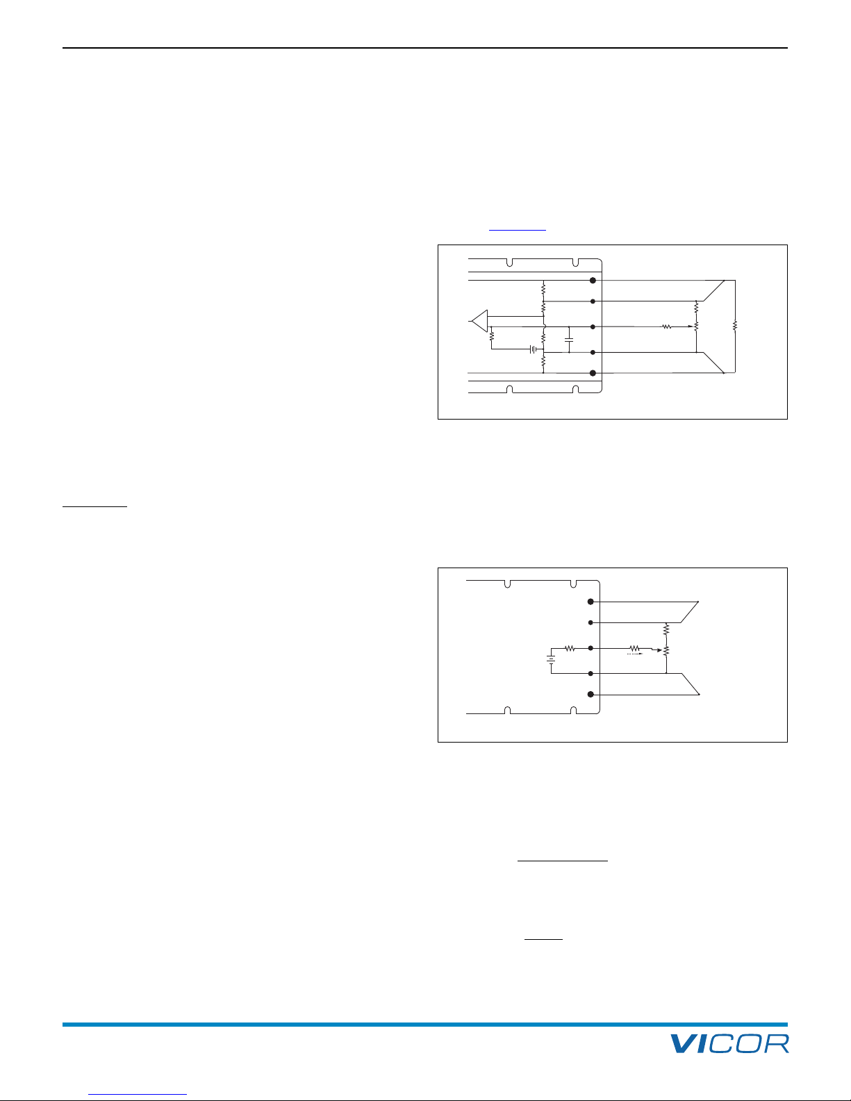
GATE IN AND GATE OUT PINS
Logic Disabl . When power is applied to the input pins,
the GATE IN pin of a Driver can be pulled low with respect
to the –IN thus turning off the output while power is still
applied to the input. (Figure 7–1)
CAUTION With offline applications –IN is not
earth ground.
In Logic Disable mode, the GATE IN pin should be driven
from either an “open collector” or electromechanical
switch that can sink 6 mA when on (GATE IN voltage less
than 0.65 V). If driven from an electromechanical switch
or relay, a 1 µF capacitor should be connected from GATE IN
to –IN to eliminate the effects of switch “bounce”. The 1 µF
capacitor may be required in all applications to provide a
“soft start” if the unit is disabled and enabled quickly. Do
not exceed a repetitive on / off rate of 1 Hz to the GATE
IN or input voltage pins.
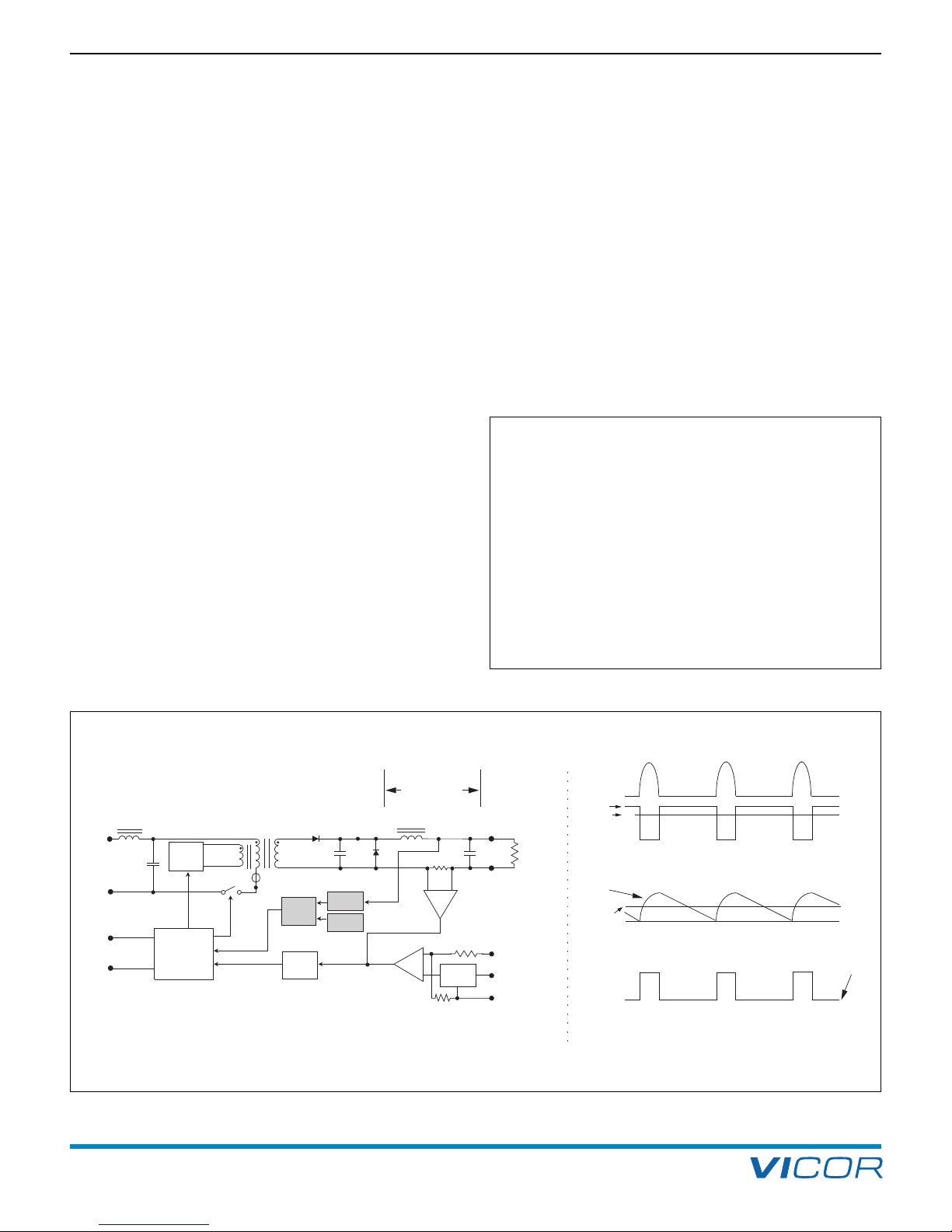
High Pow r Arrays. The pulsed signal at the GATE OUT
pin of a regulating Driver module is used to synchronously
drive the GATE IN pin of a companion Booster module to
effect power sharing between the Driver and the Booster.
(Figure 7–5) Daisy-chaining additional Boosters (i.e.,
connecting GATE OUT to GATE IN of a succeeding unit)
leads to a virtually unlimited power expansion capability.
VI-/MI-200 series modules of the same family and power
level can be paralleled (i.e., Driver, VI-260-CU with
Booster, VI-B60-CU).
In general:
• Don’t drive the GATE IN pin from an “analog”
voltage source.
• Don’t leave GATE IN pins of Booster modules
unterminated.
• Don’t overload GATE OUT; limit load to a single Vicor
module GATE IN connection, or 1 kΩ, minimum, in
parallel with 100 pF, maximum.
• Don’t skimp on traces that interconnect module –IN
pins in high power arrays. GATE IN and GATE OUT
are referenced to –IN; heavy, properly laid out traces will
minimize parasitic impedances that could interfere with
proper operation.
• Do use a decoupling capacitor across each module’s
input (see Input Source Impedance that follows).
• Do use an EMI suppression capacitor from +/– input and
output pins to the baseplate.
• Do use a fuse on each module’s + input to prevent fire
in the event of module failure. See safety agency
conditions of acceptability for the latest information on
fusing. Please see the Vicor website
for Safety Approvals.
Input Sourc Imp danc . The converter should be
connected to an input source that exhibits low AC
impedance. A small electrolytic capacitor should be
mounted close to the module’s input pins. (C3, Figure 3–1)
This will restore low AC impedance, while avoiding the
potential resonance associated with “high-Q” film
capacitors. The minimum value of the capacitor, in
microfarads, should be C (µF) = 400 ÷ Vin minimum.
Example: Vin, minimum, for a VI-260-CV is 200 V. The
minimum capacitance would be 400 ÷ 200 = 2 µF. For
applications involving long input lines or high inductance,
additional capacitance will be required.
The impedance of the source feeding the input of the
module directly affects both the stability and transient
response of the module. In general, the source impedance
should be lower than the input impedance of the module
by a factor of ten, from DC to 50 kHz.
To calculate the required source impedance, use the
following formula:
Z = 0.1(VLL)2/ Pin
where: Z is required input impedance
VLL is the low line input voltage
Pin is the input power of the module
Filters, which precede the module, should be well damped
to prevent ringing when the input voltage is applied or
the load on the output of the module is abruptly changed.
Input Transi nts. Don’t exceed the transient input
voltage rating of the converter. Input Attenuator Modules
or surge suppressors in combination with appropriate
filtering, should be used in offline applications or in
applications where source transients may be induced by
load changes, blown fuses, etc. For applications where the
input voltage may go below low line it is recommended
that an undervoltage lockout circuit be used to pull GATE
IN low to disable the converter module. The undervoltage
lockout circuit should induce a delay of at least one
second before restarting the converter module. Longer
delays will be required if external capacitance is added at
the output to insure the internal soft-start is re-initialized.
NOTE Do not allow the rate of change of the input
voltage to exceed 10 V/µs for any input voltage deviation.
The level of transient suppression required will depend on
the severity of the transients. A Zener diode, TRANSZORB™
or MOV will provide suppression of transients under 100 µs
and act as a voltage clipper for DC input transients. It may
be necessary to incorporate an LC filter for larger energy
transients. This LC filter will integrate the transient energy
while the Zener clips the peak voltages. The Q of this filter
should be kept low to avoid potential resonance problems.
See Section 14, Input Attenuator Module (IAM/ MI-IAM)
for additional information on transient suppression.
3. Module Do’s and Dont’s

Design Guide & Applications Manual
For VI-200 and VI-J00 Family DC-DC Converters and Configurable Power Supplies
VI-200 and VI-J00 Family Design Guide Rev 3.4 vicorpower.com
Page 5 of 97 Apps. Eng. 800 927.9474 800 735.6200
Output OVP. The VI-/MI-200, with the exception of
VI-/MI-J00s, has an internal overvoltage protection circuit
that monitors the voltage across the output power pins. It
is designed to latch the converter off at 115 – 135% of
rated output voltage. It is not a crowbar circuit, and if a
module is trimmed above 110% of rated output voltage,
OVP may be activated. Do not backdrive the output of
the converter module to test the OVP circuit.
CAUTION When trimming up VI-/MI-J00 modules,
additional care should be taken as an improper
component selection could result in module failure.
Improper connection of the sense leads on VI-/MI-J00
modules can also result in an excessive overvoltage
condition and module failure.
Input R v rs Voltag Prot ction. The module may be
protected against reverse input voltages by the addition of
a diode in series with the positive input, or a reverse
shunt diode with a fuse in series with the positive input.
See Section 14, the Input Attenuator Module (IAM/MI-IAM)
provides input reverse voltage protection when used with
a current limiting device (fuse).
THERMAL / MECHANICAL CONSIDERATIONS
Bas plat . Operating temperature of the baseplate, as
measured at the center mounting slot on the –IN, –OUT
side, can not exceed rated maximum. ThermMate or
thermal compound should be used when mounting the
module baseplate to a chassis or heat sink. All six
mounting holes should be used. Number six (#6) machine
screws should be torqued to 5-7 in-lbs, and use of Belville
washers is recommended.
The module pins are intended for PCB mounting either by
wave soldering to a PCB or by insertion into one of the
recommended PCB socket solutions.
CAUTION Use of discrete wires soldered directly
to the pins may cause intermittent or permanent
damage to the module; therefore, it is not
recommended as a reliable interconnection scheme
for production as a final released product. See
Section 21 for packaging options designed for
discrete wire connections (BusMod, MegaMod).
In addition, modules that have been soldered into printed
circuit boards and have subsequently been removed
should not be reused.
THERMAL AND VOLTAGE HAZARDS
Vicor component power products are intended to be used
within protective enclosures. Vicor DC-DC converters
work effectively at baseplate temperatures, which could
be harmful if contacted directly. Voltages and high
currents (energy hazard) present at the pins and circuitry
connected to them may pose a safety hazard if contacted
or if stray current paths develop. Systems with removable
circuit cards or covers which may expose the converter(s)
or circuitry connected to the converters, should have proper
guarding to avoid hazardous conditions.
EMC CONSIDERATIONS
All applications utilizing DC-DC converters must be properly
bypassed, even if no EMC standards need to be met. Bypass
IN and OUT pins to each module baseplate as shown in
Figure 3–1. Lead length should be as short as possible.
Recommended values vary depending on the front end, if
any, that is used with the modules, and are indicated on the
appropriate data sheet. In most applications, C1a – C1b is a
4,700 pF Y-capacitor (Vicor Part # 01000) carrying the
appropriate safety agency approval; C2a – C2b is a 4,700 pF
Y-capacitor (Vicor Part # 01000) or a 0.01 µF ceramic
capacitor rated at 500 V. In PCB mount applications, each of
these components is typically small enough to fit under the
module baseplate flange.
Figure 3–1 — IN and OUT pins bypassed to the module baseplate
and input cap for low AC impedance
3. Module Do’s and Dont’s
+OUT
+IN
–IN –OUT
Zero Current
Switching
Converter
C1a
C1b
C2a
C2b
C3

Design Guide & Applications Manual
For VI-200 and VI-J00 Family DC-DC Converters and Configurable Power Supplies
VI-200 and VI-J00 Family Design Guide Rev 3.4 vicorpower.com
Page 6 of 97 Apps. Eng. 800 927.9474 800 735.6200
SAFETY CONSIDERATIONS
Shock Hazard. Agency compliance requires that the
baseplate be grounded.
Fusing. Internal fusing is not provided in Vicor DC-DC
converters. To meet safety agency conditions, a fuse is
required. This fuse should be placed in the positive input
lead, not the negative input lead, as opening of the
negative input lead will cause the GATE IN and GATE OUT
to rise to the potential of the +IN lead, causing possible
damage to other modules or circuits that share common
GATE IN or GATE OUT connections.
Safety agency conditions of acceptability require module
input fusing. The VI-x7x, VI-x6x and VI-x5x require the use
of a Buss PC-Tron fuse, or other DC-rated fuse. See below
for suggested fuse ratings.
The safety approvals section of the Vicor website should
always be checked for the latest fusing and conditions of
acceptability information for all DC-DC converters
including the MegaMod family.
Package Size Required Fuse Package Size Required Fuse
VI-27x-xx PC-Tron 2.5 A VI-J7x-xx PC-Tron 2.5 A
VI-26x-xx PC-Tron 3 A VI-J6x-xx PC-Tron 3 A
VI-25x-xx PC-Tron 5 A VI-J5x-xx PC-Tron 5 A
VI-2Tx-xx PC-Tron 5A VI-JTx-xx PC-Tron 5A
VI-24x-xx 6 A / 125 V VI-J4x-xx PC-Tron 5A
VI-2Nx-xx 8A / 125 V VI-JNx-xx PC-Tron 5A
VI-23x-xx 8 A /125 V VI-J3x-xx PC-Tron 5A
VI-22x-xx 8 A / 60 V VI-J2x-xx PC-Tron 5A
VI-2Wx-xx 12 A / 50 V VI-JWx-xx 8 A / 60 V
VI-21x-xx 12 A / 32 V VI-J1x-xx 8 A / 60 V
VI-2Vx-xx 12 A / 32 V VI-J0x-xx 8 A / 60 V
VI-20x-xx 12 A / 32 V
Acceptable Fuse Types and Current Rating for the VI-200 and VI-J00 Family of Converters
3. Module Do’s and Dont’s

Design Guide & Applications Manual
For VI-200 and VI-J00 Family DC-DC Converters and Configurable Power Supplies
VI-200 and VI-J00 Family Design Guide Rev 3.4 vicorpower.com
Page 7 of 97 Apps. Eng. 800 927.9474 800 735.6200
FOLDBACK CURRENT LIMITING
The VI-/MI-200 modules with output voltages of 5 V or
3.3 V incorporate foldback current limiting. (Figure 4–1) In
this mode, the output voltage remains constant up to the
current knee, (Ic), which is 5 – 25% greater than full-rated
current, (Imax). Beyond Ic, the output voltage falls along
the vertical line Ic– Ifb until approximately 2 V. At ≤2 V, the
voltage and current folds back to short circuit current
point (20 – 80% of Imax). Typically, modules will
automatically recover when overcurrent is removed.
When bench testing modules with foldback current limiting,
use a constant resistance load as opposed to a constant
current load. Some constant current loads have the ability
to pull full current at near zero volts. This may cause a
latchup condition. Also when performing a short circuit
test it is recommended to use a mercury wetted relay to
induce the output short as other methods may induce
switch bounce that could potentially damage the converter.
STRAIGHT LINE CURRENT LIMITING
The VI-/MI-200 modules with output voltages greater
than 5 V, 2 V (VI-/MI-200 only) and all VI-/MI-J00
modules incorporate a straight-line type current limit.
(Figure 4–2) As output current is increased beyond Imax,
the output voltage remains constant and within its
specified limits up to a point, Ic, which is 5 – 25% greater
than rated current, (Imax). Beyond Ic, the output voltage
falls along the vertical line to Isc. Typically, modules will
automatically recover after overcurrent is removed.
2 V
V
out
Ic
Ifb
Imax
Iout
Ishort circuit
Vout
Ishort circuit
Ic
Imax
Iout
4. Overcurrent Protection
Figure 4–1 — Foldback current limiting Figure 4–2 — Straight-line current limiting

Design Guide & Applications Manual
For VI-200 and VI-J00 Family DC-DC Converters and Configurable Power Supplies
VI-200 and VI-J00 Family Design Guide Rev 3.4 vicorpower.com
Page 8 of 97 Apps. Eng. 800 927.9474 800 735.6200
OVERVIEW
Specifications such as efficiency, ripple and input voltage
range are a function of output voltage settings. As the
output voltage is trimmed down, efficiency goes down;
ripple as a percent of Vout goes up and the input voltage
range widens since input voltage dropout (loss of regulation)
moves down. As the units are trimmed up, the reverse of
the above effects occurs.
All converters have a fixed current limit. The overvoltage
protection setpoint is also fixed; trimming the output
voltage does not alter its setting. As the output voltage is
trimmed down, the current limit setpoint remains constant.
Therefore, in terms of output power, if the unit is trimmed
down, available output power drops accordingly.
The output voltage of most Vicor converters can be
trimmed +10%, –50%. Certain modules have restricted
trim ranges. Consult the latest datasheet for details.
Do not attempt to trim the module output voltage more
than +10%, as overvoltage shut down may occur. Do not
exceed maximum rated output power when the module is
trimmed up.
CAUTION When trimming up VI-/ MI-J00 converter
modules, additional care should be taken as an
improper component selection could result in module
failure. Improper connection of the sense leads on
VI-/MI-J00 converter modules can also result in an
excessive overvoltage condition and module failure.
The following procedures describe methods for output
voltage adjustment (–10 to +10% of nominal) of the
VI-/MI-200, VI-/MI-J00, ComPAC/MI-ComPAC, FlatPAC
and MegaMod / MI-MegaMod Families.
Modules with nominal 3.3 V outputs and above have
the 2.5 V precision reference and 10 k internal resistor.
For trim resistor calculations on modules with 2.0 V
outputs use 0.97 V in place of the 2.5 V reference
and substitute 3.88 kΩfor the internal 10 kΩresistor.
Resistors are 0.25 W. When trimming down any module,
always maintain a minimum preload of at least 1% of
rated output power and in some cases up to 10% may be
required. For more specific information on trimming down
a specific module, please consult Vicor’s Applications
Engineering Department at (800) 927-9474.
RESISTIVE ADJUSTMENT PROCEDURE
To achieve a variable trim range, an external resistor
network must be added. (Figure 5–1)
Exampl 1. For trimming –10% to +10% with a standard
off-the-shelf 10 kΩpotentiometer (R7), values for resistors
R6 and R8 need to be calculated.
Resistor R6 limits the trim down range. For a given
percentage, its value is independent of output voltage.
Refer to Table 5–1, for limiting resistor values.
TRIMMING DOWN –10%
A 10% drop of the 2.5 V reference at the TRIM pin is
needed to effect a 10% drop in the output voltage.
(Figure 5–2)
V1= 2.5 V – 10% = 2.25 V
Therefore:
IR5 =(2.5 V – 2.25 V) = 25 µA
10 kΩ
Since IR5 = IR6 = 25 µA:
R6 = 2.25 V = 90 kΩ
25 µA
This value will limit the trim down range to –10% of
nominal output voltage.
5. Output Voltage Trimming
Figure 5–1 — External resistive network for variable trimming
+OUT
+SENSE
–OUT
R3
–
+
C1
Load
[a]For Vout <3.3 V, R5 = 3.88 k and internal reference = 0.97 V.
Error Amp
R1 47 Typ.
R4 27 Typ.
R2
R5 10 k [a]
TRIM R6
–SENSE
R8
R7
2.5 V[a]
R6
TRIM
–SENSE
–OUT
R7 10 kΩ POT
R5 10 kΩ[a]
(internal)
V1
R8
IR6
2.5 V[a]
reference
(internal)
[a] For Vout <3.3 V, R5 = 3.88 kΩand internal reference = 0.97 V.
+OUT
+SENSE
–SENSE
Figure 5–2 — Circuit diagram “Trim Down”

Design Guide & Applications Manual
For VI-200 and VI-J00 Family DC-DC Converters and Configurable Power Supplies
VI-200 and VI-J00 Family Design Guide Rev 3.4 vicorpower.com
Page 9 of 97 Apps. Eng. 800 927.9474 800 735.6200
5. Output Voltage Trimming
TRIMMING UP +10%
To trim 10% above the nominal output voltage, the
following calculations are needed to determine the value
of R8. This calculation is dependent on the output voltage
of the module. A 12 V output will be used as an example.
(Figure 5–3)
It is necessary for the voltage at the TRIM pin to be 10%
greater than the 2.5 V reference. This offset will cause the
error amplifier to adjust the output voltage up 10% to 13.2 V.
V1= 2.5 V + 10% = 2.75 V
IR5 =(2.75 V – 2.5 V) = 25 µA
10 kΩ
Since IR5 = IR6 ,
the voltage drop across R6 = (90 kΩ) (25 µA) = 2.25 V.
Therefore, V2= 2.75 V + 2.25 V = 5 V. The current
through R7 (10 kΩpot) is:
IR7 =V2=5 = 500 µA
R7 10 k
Using Kirchoff’s current law:
IR8 = IR7 + IR6 = 525 µA
Thus, knowing the current and voltage, R8 can be
determined:
VR8 = (Vout + 10%) – V2= 13.2 V – 5 V = 8.2 V
R8 = (8.2 V) = 15.6 kΩ
525 µA
This resistor configuration allows a 12 V output module
to be trimmed up to 13.2 V and down to 10.8 V. Follow
this procedure to determine resistor values for other
output voltages.
FIXED TRIM
Converters can be trimmed up or down with the addition
of one external resistor, either Ru for programming up or
Rd for programming down. (Figure 5–4)
Exampl 2. Fixed Trim Up (12 V to 12.6 V).
To determine Ru, the following calculation must be made:
2.5 V + 5% = 2.625 V
VR5= VTRIM – Vref
VR5= 2.625 – 2.5 = 0.125 V
Knowing this voltage, the current through R5 can be found:
IR5 =VR5 =0.125 = 12.5 µA
R5 10 kΩ
VRu = 12.6 V – 2.625 V = 9.975 V
Ru = 9.975 = 798 kΩ
12.5 µA
Connect Ru from the TRIM pin to the +SENSE. Be sure to
connect the resistor to the +SENSE, not the +OUT, or
drops in the positive output lead as a function of load will
cause apparent load regulation problems.
Exampl 3. –25% Fixed Trim Down (24 V to 18 V).
The trim down methodology is identical to that used in
Example 2, except that it is utilized to trim the output of a
24 V module down 25% to 18 V. The voltage on the
TRIM pin must be reduced 25% from its nominal setting
of 2.5 V. This is accomplished by adding a resistor from
the TRIM pin to –SENSE.
2.5 V – 25% = 1.875 V
VR5 = Vbandgap – VTRIM
= 2.5 V – 1.875 V = 0.625 V
I
V2
R6 90 kΩ
TRIM
+ SENSE
–SENSE
– OUT
R5 10 kΩ[a]
(internal)
V1
R8R8
R7 10 kΩPOT
500 µA
25 µA
2.5 V[a]
reference
(internal)
+ OUT
[a]For Vout <3.3 V, R5 = 3.88 kΩand internal reference = 0.97 V.
Figure 5–3 — Circuit diagram “Trim Up”
TRIM
+ OUT
+ SENSE
– SENSE
– OUT
Rd
Ru Trim Resistor for UP
Programming
Trim Resistor for DOWN
Programming
or
2.5 V[a]
reference
(internal)
R5 10 k [a]
(internal)
[a]For Vout <3.3 V, R5 = 3.88 k and internal reference = 0.97 V.
Figure 5–4 — Fixed trimming

Design Guide & Applications Manual
For VI-200 and VI-J00 Family DC-DC Converters and Configurable Power Supplies
VI-200 and VI-J00 Family Design Guide Rev 3.4 vicorpower.com
Page 10 of 97 Apps. Eng. 800 927.9474 800 735.6200
Knowing this voltage, the current through R5 can be found:
IR5 =VR5=0.625 = 62.5 µA
R5 10 kΩ
The voltage across the resistor, Rd, and the current
flowing through it are known:
Rd = (2.5 V – 0.625 V) = 30 kΩ
62.5 µA
Connect Rd (Figure 5–4) from the TRIM pin to the –SENSE
of the module. Be sure to connect the resistor to the
–SENSE, not the –OUT, or drops in the negative output
lead as a function of load will cause apparent load
regulation problems.
DYNAMIC ADJUSTMENT PROCEDURE
Output voltage can also be dynamically programmed by
driving the TRIM pin from a voltage or current source;
programmable power supplies and power amplifier
applications can be addressed in this way. For dynamic
programming, drive the TRIM pin from a source referenced
to the negative sense lead, and keep the drive voltage in
the range of 1.25 – 2.75 V. Applying 1.25 – 2.5 V on the
TRIM pin corresponds to 50 – 100% of nominal output
voltage. For example, an application requires a +10, 0%
(nominal), and a –15% output voltage adjustment for a 48 V
output converter. Referring to the table below, the voltage
that should be applied to the trim pin would be as follows:
VTRIM VOUT Change from nominal
2.125 40.8 –15%
2.5 48 0
2.75 52.8 +10%
The actual voltage range is further restricted by the
allowable trim range of the converter. Voltages in excess
of 2.75 V (+10% over nominal) may cause overvoltage
protection to be activated. For applications where the
module will be programmed on a continuous basis the
slew rate should be limited to 30 Hz sinusoidal.
TRIMMING ON THE WEB (VICORPOWER.COM)
Trim valu s ar calculat d automatically. Design
Calculators are available on Vicor’s website in the
PowerBenchTM section at
www.vicorpower.com/powerbench.
Resistor values can be easily determined for fixed trim up,
fixed trim down and for variable trimming applications.
In addition to trimming information, the website also
includes design tips, applications circuits, EMC
suggestions, thermal design guidelines and PDF data
sheets for all available Vicor products.
Percent Resistance
–5 % 190 kΩ
–10 % 90 kΩ
–15 % 56.7 kΩ
–20 % 40 kΩ
–25 % 30 kΩ
–30 % 23.3 kΩ
–35 % 18.6 kΩ
–40 % 15 kΩ
–45 % 12.2 kΩ
–50 % 10 kΩ
Vnom V (Desired) Trim Resistor [a]
5V 4.5 V 90.9 kΩ
3.3 V 19.6 kΩ
2.5 V 10.0 kΩ
15 V 13.8 V 115 kΩ
24 V 20 V 49.9 kΩ
48 V 40 V 49.9 kΩ
36 V 30.1 kΩ
Vnom V (Desired) Trim Resistor [a]
5V 5.2 V 261 kΩ
5.5 V 110 kΩ
12 V 12.5 V 953 kΩ
13.2 V 422 kΩ
15 V 15.5 V 1.62 MΩ
16.5 V 562 kΩ
24 V 25 V 2.24 MΩ
48 V 50 V 4.74 MΩ
Table 5–1 — Values for trim down by percentage (Refer to product
data sheet for allowable trim ranges at vicorpower.com)
Values for Trim Down by Percentage
Fixed Trim Down
Table 5–2a — Values for fixed trim down by voltage
Fixed Trim Up
Table 5–2b — Values for fixed trim up by voltage
[a] Values listed in the tables are the closest standard 1% resistor values.
5. Output Voltage Trimming

Design Guide & Applications Manual
For VI-200 and VI-J00 Family DC-DC Converters and Configurable Power Supplies
VI-200 and VI-J00 Family Design Guide Rev 3.4 vicorpower.com
Page 11 of 97 Apps. Eng. 800 927.9474 800 735.6200
OVERVIEW
A number of GATE IN pins may be connected for remote
shut down and logic disable. (Figure 6-1) Diodes D1 and
D2 provide isolation and prevent multiple failures if the
GATE IN of a module becomes shorted to the +IN. The
Zener diodes Z1, Z2 and capacitors C1, C2 attenuate
transient voltage spikes caused by differential inductance
in the negative lead. Capacitors C1 and C2 will also
lengthen turn-on time. SW1 is a mechanical or solid state
switch that is used to disable both Driver modules. C3 is
used to minimize the effects of “switch bounce” associated
with mechanical devices.
NOTE GATE IN voltage needs to be <0.65 V
referenced to –IN to ensure modules are disabled.
+IN
–IN
GATE
OUT
GATE
IN
+IN
–IN
GATE
OUT
GATE
IN
Vicor
DC-DC Converter
F1
C1
Z1
C3
SW1 F2
DISABLE
D2
Z2 C2
D1
Vicor
DC-DC Converter
6. Multiple GATE IN Connections
C1, C2, C3 = 1 µF
Z1, Z2 = 15 V (1N5245B)
D1, D2 = Small signal diode (1N4148) [a]
[a] For bus voltages greater than 75 V,
a 1N4006 diode should be used.
NOTE The –IN to –IN input lead should be kept as short as possible to minimize differential inductance.
Heavy lines indicate power connections. Use suitably sized conductors.
Opto-couplers or relays should be used to isolate GATE IN connections, if the converters are on
separate boards or the negative input lead’s impedance is high.
Figure 6–1 — Protection for multiple GATE IN connections

Design Guide & Applications Manual
For VI-200 and VI-J00 Family DC-DC Converters and Configurable Power Supplies
VI-200 and VI-J00 Family Design Guide Rev 3.4 vicorpower.com
Page 12 of 97 Apps. Eng. 800 927.9474 800 735.6200
Logic Disabl . (Figure 7–1) The GATE IN pin of the
module may be used to turn the module on or off. When
GATE IN is pulled low (<0.65 V 6 mA, referenced to
–Vin), the module is turned off. When GATE IN is floating
(open collector), the module is turned on. The open circuit
voltage of the GATE IN pin is less than 10 V. This applies
to VI-/MI-200, VI-/MI-J00 and MegaMod / MI-MegaMod
Family modules.
Output Voltag Programming. (Figure 7–2) Consult
Vicor’s Applications Engineering Department before
attempting large signal applications at high repetition
rates due to ripple current considerations with the internal
output capacitors. This applies to VI-/MI-200, VI-/MI-J00,
ComPAC/MI-ComPAC, FlatPAC and MegaMod/
MI-MegaMod Family modules.
Vout =Vtrim x Vnom
2.5
N gativ Inputs (with positiv ground). (Figure 7–3)
Vicor modules have isolated inputs and outputs making
negative input configurations easy. Fusing should always
be placed in the positive lead.
R mot S nsing. (Figure 7–4) Output voltage between
+OUT and –OUT must be maintained below 110% of
nominal. Do not exceed 0.25 V drop in negative return as
the current limit setpoint is moved out proportionately.
The sense should be closed at the module if remote
sensing is not desired. Applies to VI-/MI-200, VI-/MI-J00,
ComPAC/MI-ComPAC, FlatPAC and MegaMod/
MI-MegaMod Family modules. Excessively long sense leads
and / or excessive external capacitance at the load may
result in module instability. Please consult Vicor
Applications Engineering for compensation methods.
–OUT
–S
+S
+OUT
+IN
GAT E
IN
GAT E
OUT
–IN
Zero Current
Switching
Converter
Driver
+
–
16
TLP798G
Agilent 6N139
Load
25TRIM
1µF
7. Application Circuits / Converter Array Design Considerations
Figure 7–1 — Logic disable
–OUT
–S
TRIM
+S
+OUT
+IN
GATE
IN
GATE
OUT
–IN
Zero Current
Switching
Converter
Driver
+
–Load
+
–
Figure 7–2 — Output voltage programming
–OUT
–S
TRIM
+S
+OUT
+IN
GATE
IN
GATE
OUT
–IN
Zero Current
Switching
Converter
Driver
+
–Load
Figure 7–3 — Negative inputs (with positive ground)
–OUT
–S
TRIM
+S
+OUT
+IN
GATE
IN
GATE
OUT
–IN
Zero Current
Switching
Converter
Driver
+
–Load
• • •• • •
• • •• • •
• • •• • •
• • •• • •
Figure 7–4 — Remote sensing

Design Guide & Applications Manual
For VI-200 and VI-J00 Family DC-DC Converters and Configurable Power Supplies
VI-200 and VI-J00 Family Design Guide Rev 3.4 vicorpower.com
Page 13 of 97 Apps. Eng. 800 927.9474 800 735.6200
Parall l Boost. (Figure 7–5) U.S. Patent #4,648,020 —
other patents pending. To retain accurate power sharing
between a Driver and (n) number of Boosters, provide
adequate input and output power bussing. This applies to
VI-/MI-200 and MegaMod / MI-MegaMod Family
modules. See Module Do’s and Don’ts for recommended
external components. (Section 3)
Programmabl Curr nt Sourc . (Figure 7–6) Module
output voltage should not exceed the rated voltage of the
operational amplifier. This applies to VI-/MI-200,
VI-/MI-J00, ComPAC/ MI-ComPAC, FlatPAC and
MegaMod/MI-MegaMod Family modules.
NOTE When using a VI-J00 module, the TRIM pin
voltage should be clamped to 2.75 V to avoid
damage to the module. This corresponds to the
maximum trim up voltage. This circuit or functional
equivalent must be used when charging batteries.
Do not exceed the nominal current ratings of the
converter. Example,
Pout
Vnominal
Dual Output Voltag s. (Figure 7–7) Vicor modules have
isolated outputs so they can easily be referenced to a
common node creating positive and / or negative rails.
7. Application Circuits / Converter Array Design Considerations
Figure 7–5 — Parallel boost. U.S. Patent #4,64 ,020 — other
patents pending.
–OUT
–S
TRIM
+S
+OUT
+IN
GAT E
IN
GAT E
OUT
–IN
Zero Current
Switching
Converter
#1
Driver
VI-2xx-xx
+
–
–OUT
–S
TRIM
+S
+OUT
+IN
GAT E
IN
GAT E
OUT
–IN
Zero Current
Switching
Converter
#n
Booster
VI-Bxx-xx
Load
Figure 7–6 — Programmable current source
–OUT
-S
TRIM
+S
+OUT
+IN
GATE
IN
GATE
OUT
–IN
Zero Current
Switching
Converter
Driver
+
–Load
V Control
0.1 V/A
1K OP
AMP
–
+
1K 1K
0.05 Ω
1K
0.01
I
10 µF
–OUT
–S
TRIM
+S
+OUT
+IN
GATE
IN
GATE
OUT
–IN
Zero Current
Switching
Converter
Driver
+
–Load requiring
positive output
–OUT
–S
TRIM
+S
+OUT
+IN
GATE
IN
GATE
OUT
–IN
Zero Current
Switching
Converter
Driver
+
–
Load requiring
negative output
Figure 7–7 — Dual output voltages

Design Guide & Applications Manual
For VI-200 and VI-J00 Family DC-DC Converters and Configurable Power Supplies
VI-200 and VI-J00 Family Design Guide Rev 3.4 vicorpower.com
Page 14 of 97 Apps. Eng. 800 927.9474 800 735.6200
OVERVIEW
The VI-/MI-200 Family of DC-DC converters are available
as Driver or Booster modules. The Driver can be used as a
stand alone module, or in multi-kilowatt arrays by adding
parallel Boosters. Booster modules do not contain
feedback or control circuitry, so it is necessary to connect
the Booster GATE IN pin to the preceding Driver or
Booster GATE OUT, to synchronize operation. Drivers and
Boosters have identical power trains, although Drivers
close the voltage loop internally while Boosters do not.
The concept behind Driver / Booster operation is that two
or more ZCS power trains driven at the same frequency
will inherently load-share if their inputs and outputs are
tied together. Slaved modules require only one connection
between units when their outputs are connected
together; no trimming, adjustments or external
components are required to achieve load sharing. The
load sharing is dynamic and typically within 5%.
For additional information, refer to Electrical Considerations
– High Power Arrays in the Module Do’s and Don’ts.
(Section 3)
IMPORTANT It is important to remember that when
using Boosters, the input voltage, output voltage and
output power of the Boosters must be the same as
the Driver.
Whenever power supplies or converters are operated in a
parallel configuration—for higher output power, fault
tolerance, or both—current sharing is an important
consideration. Most current-sharing schemes employed
with power converters involve analog approaches. One
analog method artificially increases the output impedance
of the converter modules, while another actually senses
the output current of each module and forces all of the
currents to be equal by feedback control.
Synchronous current sharing offers an alternative to
analog techniques. In a synchronous scheme, there is no
need for a current-sensing or current-measuring device on
each module. Nor is there a need to artificially increase
output impedance, which compromises load regulation.
There are advantages and disadvantages associated with
each approach to current sharing. In choosing the best
approach for a given application, designers should be
aware of the tradeoffs as well as tips for implementing a
successful design.
Most paralleled power components, such as transistors,
rectifiers, power conversion modules, and offline power
supplies, will not inherently share the load. With power
converters, one or more of the converters will try to
assume a disproportionate or excessive fraction of the
load unless forced current-sharing control is designed into
the system.
One converter, typically the one with the highest output
voltage, may deliver current up to its current limit setting,
which is beyond its rated maximum. Then, the voltage will
drop to the point where another converter in the array—
the one with the next highest voltage—will begin to
deliver current. All of the converters in an array may
Figure 8–1 — Parallel array
INPUT LOAD
+S
TRIM
–S
–OUT
+IN
GATE
IN
GATE
OUT
–IN
+S
TRIM
–S
–OUT
+IN
GATE
IN
GATE
OUT
–IN
+S
TRIM
–S
–OUT
+IN
GATE
IN
GATE
OUT
–IN
+
–
Zero-Current-
Switching
Driver
VI-2xx-xx
Zero-Current-
Switching
Booster
VI-Bxx-xx
Zero-Current-
Switching
Booster
VI-Bxx-xx
+OUT
+OUT
+OUT
8. Using Boosters and Parallel Arrays

Design Guide & Applications Manual
For VI-200 and VI-J00 Family DC-DC Converters and Configurable Power Supplies
VI-200 and VI-J00 Family Design Guide Rev 3.4 vicorpower.com
Page 15 of 97 Apps. Eng. 800 927.9474 800 735.6200
deliver some current, but the load will be shared unequally.
With built-in current limiting, one or more of the converters
will deliver current up to the current limit (generally 15 or
20% above the module’s rated maximum), while other
converters in the array supply just a fraction of load.
Consider a situation where one module in a two-module
array is providing all of the load. If it fails, the load on the
second module must go from no load to full load. During
that time, the output voltage is likely to droop temporarily.
This could result in system problems, including shutdown
or reset.
On the other hand, if both modules were sharing the load
and one failed, the surviving module would experience a
much less severe transient (one-half to full load). Also, the
output voltage would be likely to experience no more
than a slight momentary droop. The dynamic response
characteristic of all forward converters, resonant or pulse-
width modulated, is degraded when the load is stepped
from zero (no load) where the output inductor current is
discontinuous.
In the same two-module array example, the module
carrying all of the load also is generating all of the heat.
That results in a much lower mean time between failure
for that module. An often-quoted rule of thumb says that
for each 10°C increase in operating temperature, average
component life is cut in half.
In a current-sharing system, the converters or supplies all
run at the same temperature. This temperature is lower
than that of the hot-running (heavily loaded) modules in
a system without current sharing. Furthermore, same-
temperature operation means that all of the modules in
a current-sharing arrangement age equally.
Current sharing, then, is important because it improves
system performance. It optimizes transient and dynamic
response and minimizes thermal problems, which improves
reliability and helps extend the lifetimes of all of the
modules in an array. Current sharing is an essential
ingredient in most systems that use multiple power supplies
or converters to achieve higher output power or fault
tolerance.
When parallel supplies or converters are used to increase
power, current sharing is achieved through a number of
approaches. One scheme simply adds resistance in series
with the load. A more practical variant of that is the
“droop-share” method, which actively causes the output
voltage to drop in response to increasing load.
Nevertheless, the two most commonly used approaches
to paralleling converters for power expansion are Driver /
Booster arrays and analog current-sharing control. They
appear to be similar, but the implementation of each is
quite different.
Driver / Booster arrays usually contain one intelligent
module or Driver, and one or more power-train-only
modules or Boosters. Analog current-sharing control
involves paralleling two or more identical modules, each
containing intelligence.
One of the common methods of forcing load sharing in
an array of parallel converters is to sense the output
current of each converter and compare it to the average
current. Then, the output of a given converter is adjusted
so that its contribution is equal to the average. This is
usually accomplished by current-sense resistors in series
with the load, a sensing amplifier for each converter
module, and a summing amplifier. Load sharing is
accomplished by actively trimming the output voltage
using TRIM or SENSE pins.
Occasionally, a designer is tempted to avoid the expense
of a current-sense resistor by using the IR drops in the
wire as a means of sensing the current. Unfortunately,
there are a number of negative issues associated with
that idea. First of all, there’s the temperature coefficient
of copper. As the wire heats up, its resistance increases,
negating its value as a stable current-sensing device.
Second, there are oxidation and corrosion issues, which
also cause parametric changes. Consequently, a high-
precision current-sensing device, such as a precision
resistor, is a must.
The resistor values typically range from a few milliohms
up to about 100 mΩ, depending on the power level or
current range of operation. Selecting the right value
requires a tradeoff between power dissipation and
sensitivity (signal-to-noise ratio or noise immunity). The
larger the resistor value, the better the noise immunity—
and the greater the power dissipation.
Determining the size of the resistor needed to generate a
signal above the noise can be a bit tricky. Another
potential pitfall with this (or, for that matter, any other)
approach is the need for good electrical and mechanical
design and layout. This requires adequate trace widths,
minimized trace lengths, and decoupling to reduce noise.
An experienced designer should have no difficulty with
this, but it is an area rich with opportunities for error.
The droop-share method artificially increases the output
impedance to force the currents to be equal.
It’s accomplished by injecting an error signal into the
control loop of the converter, causing the output voltage
to vary as a function of load current. As load current
increases, output voltage decreases. All of the modules
will deliver approximately the same current because they
are all being summed into one node.
If one supply is delivering more current than another
supply, its output voltage will be slightly forced down so
8. Using Boosters and Parallel Arrays

Design Guide & Applications Manual
For VI-200 and VI-J00 Family DC-DC Converters and Configurable Power Supplies
VI-200 and VI-J00 Family Design Guide Rev 3.4 vicorpower.com
Page 16 of 97 Apps. Eng. 800 927.9474 800 735.6200
that it will be delivering equal current for an equal voltage
at the summing node. A simple implementation of the
droop-share scheme uses the voltage dropped across an
ORing diode, which is proportional to current, to adjust
the output voltage of the associated converter. (Figure 8–2)
Droop share has advantages and disadvantages. One of
the advantages is that it can work with any topology. It’s
also fairly simple and inexpensive to implement. Though, a
major drawback is that it requires that the current be
sensed. A current-sensing device is needed in each of the
converters or power supplies. Additionally, a small penalty
is paid in load regulation, though in many applications this
isn’t an issue.
In general, mixing and matching converters isn’t
recommended—especially those with incompatible
current-sharing schemes. The droop-share method,
however, is more forgiving in this regard than any of the
other techniques. With a little external circuitry, current
sharing can be achieved using arrays constructed from
different converter models or even from different suppliers.
Most systems can employ the Driver / Booster (or master /
slave) array for increased power. (Figure 8–3) The Driver is
used to set and control output voltage, while Booster
modules, as slaves to the master, are used to extend
output power to meet system requirements.
Driver / Booster arrays of quasi-resonant converters with
identical power trains inherently current share because the
per-pulse energy of each converter is the same. If the
inputs and outputs are tied together and the units operate
at the same frequency, all modules will deliver equal
current (within component tolerances).
The single intelligent module in the array determines the
transient response, which does not change as modules
are added. Slaved modules require only one connection
between units when their outputs are connected. No
trimming, adjustments, or external components are
required to achieve load sharing. The load sharing is
dynamic and usually guaranteed within 5%. It’s important
to remember that when using Boosters, the input and
output voltage and output power specifications of the
Boosters must be the same as the Driver.
Driver / Booster arrays have two advantages. They have
only a single control loop, so there are no loop-within-a-
loop stability issues. And, they have excellent transient
response. However, this arrangement isn’t fault tolerant.
If the Driver module fails, the array won’t maintain its
output voltage.
Analog current-sharing control involves paralleling two or
more identical modules, each containing intelligence. The
circuit actively adjusts the output voltage of each supply
so the multiple supplies deliver equal currents. This method,
though, has a number of disadvantages. Each converter in
the array has its own voltage regulation loop, and each
requires a current-sensing device and current-control loop.
Analog current-sharing control does support a level of
redundancy. But it’s susceptible to single-point failures
within the current-sharing bus that at best can defeat
current sharing, and at worst can destroy every module in
the array. The major reason for this is the single-wire
galvanic connection between modules.
Current sharing is an essential element in fault-tolerant
arrays. Yet regardless of the approach, there is an inherent
–OUT
–S
TRIM
+S
+OUT
+IN
GATE
IN
GATE
OUT
–IN
–OUT
–S
TRIM
+S
+OUT
+IN
GATE
IN
GATE
OUT
–IN
Return
Zero Current
Switching
Converter
#1
Driver
Zero Current
Switching
Converter
#n
Driver
+V
IN
+V
OUT
–V
IN
Figure 8–2 — Droop-share current sharing artificially increases converter output impedance to force the currents to be equal. Diodes on the
output of each converter provide current sensing and fault protection.
8. Using Boosters and Parallel Arrays

Design Guide & Applications Manual
For VI-200 and VI-J00 Family DC-DC Converters and Configurable Power Supplies
VI-200 and VI-J00 Family Design Guide Rev 3.4 vicorpower.com
Page 17 of 97 Apps. Eng. 800 927.9474 800 735.6200
cost incurred by the addition of at least one redundant
converter or supply.
Incidentally, most applications today that require fault
tolerance or redundancy also require Hot-Swap capability
to ensure continuous system operation. Hot-swappable
cards must be designed so the operator won’t come in
contact with dangerous potentials and currents.
It’s also essential that when a module fails, the failure is
detected and identified by an alarm or notice to provide
service. A Hot-Swap system must ensure that during
swap-out, there is minimal disturbance of the power bus.
Specifically, the affected voltage bus must not drop
enough to cause errors in the system, either on the input
bus or the output bus.
A power-supply failure can cripple an entire system, so the
addition of a redundant converter or supply is often
justified by the need to keep the system operating.
Adding an extra module (N+1) to a group of paralleled
modules will significantly increase reliability with only a
modest increase in cost.
The implementation of redundant converters is
determined in part by the available space and cost
requirements. For example, two 200 W full-size modules
could be used to provide a 400 W output with an
additional 200 W module for 2+1 redundancy (a total of
600 W in a volume of about 16.5 in3).
Alternatively, four 100 W half-size modules might be used
with a fifth 100 W module to provide 4+1 redundancy (a
total of 500 W and 14 in3). Although the second solution
uses less space, it increases the accumulated failure rate
because it employs more converters, more ORing diodes,
more monitoring circuitry, and more assembly.
ORing diodes may be inserted in series with the output
of each module in an N+1 array to provide output fault
tolerance. (Figure 8–2) They’re important in a redundant
power system to maintain fault isolation. Without them,
a short-circuit failure in the output of one converter could
bring down the entire array.
But ORing diodes add losses to the power system,
reducing overall efficiency and decreasing reliability. To
ameliorate the negative effect on efficiency, ORing diodes
should run hot, thereby reducing forward voltage drop
and increasing efficiency. Reverse leakage current will be
an issue only if the output of a converter shorts and the
diode is reverse biased. This is an important consideration
with regard to operating temperature.
8. Using Boosters and Parallel Arrays
INPUT LOAD
+ Sense
Trim
–Sense
GATE
IN
–IN
Zero-Current-
Switching Driver
+OUT
GATE
OUT
+IN
–OUT
+Sense
Trim
–Sense
–IN
Zero-Current-
Switching Booster
+OUT
+IN
–OUT
+Sense
Trim
–Sense
–IN
Zero-Current-
Switching Booster
+OUT
+IN
–OUT
+VIN
-VIN
GATE
IN
GATE
OUT
GATE
IN
GATE
OUT
Figure 8–3 — Most converters can use the Driver / Booster array to increase output power. Driver / Booster arrays usually contain one
intelligent module or Driver, and one or more power-train-only modules or Boosters.

Design Guide & Applications Manual
For VI-200 and VI-J00 Family DC-DC Converters and Configurable Power Supplies
VI-200 and VI-J00 Family Design Guide Rev 3.4 vicorpower.com
Page 18 of 97 Apps. Eng. 800 927.9474 800 735.6200
+IN
GATE
IN
GATE
OUT
–IN
+OUT
+S
TRIM
–S
–OUT
C2
C1
C2 C3
C3
C1 = 100 µF
C2 = 4,700 pF
C3 = 0.01 µF
Conditions:
Light Load = 3 A
Nominal Line = 48 V Nominal Load = 15 A
Full Load = 30 A
Figure 9–1 — Conducted input noise, no additional filtering
3 Amp Load 15 Amp Load 30 Amp Load
CONDUCTED NOISE
Conducted noise is the AC current flowing between the
source voltage and the power supply. It includes both
common-mode and differential-mode noise. Vicor zero-
current-switching converters are 20 – 40 dB lower in
conducted noise than a traditional board-mounted PWM
converter; however, if a specific EMC specification such as
FCC or VDE must be met, additional filtering may be required.
Since the noise generated is ten to a hundred times lower
than fixed frequency converters, an existing filter should
provide equal or better performance when the conditions
in the Module Do’s and Don’ts section are followed.
(Section 3)
In the event the system does not contain an existing filter,
the following will provide valuable information relative to
the attainment of system conducted noise objectives.
System requirements, such as Tempest (military) or UL544/
EN60601 (medical), require a somewhat different approach.
Medical requirements vary as a function of the application
and country — please contact Vicor Applications
Engineering for additional details.
Common-Mod Nois with No Additional Filt ring.
Common mode conducted noise current is the
unidirectional (in phase) component in both the +IN and
–IN pins to the module. This current circulates from the
converter via the power input leads to the DC source and
returns to the converter via the grounded baseplate or
output lead connections. This represents a potentially
large loop cross-sectional area which, if not effectively
controlled, can generate magnetic fields. Common-mode
noise is a function of the dv/dt across the main switch in
the converter and the effective input to baseplate and
input to output capacitance of the converter.
The most effective means to reduce common-mode current
is to bypass both input leads to the baseplate with
Y-capacitors (C2), keeping the leads short to reduce
parasitic inductance. Additionally, a common-mode choke
(L1) is usually required to meet FCC/VDE A or B. (Figure
9–2)
9. EMC Considerations
Conducted Noise vs. Load
Typical Vicor Module
48 V Input, 5 V Output (VI-230-CV)

Design Guide & Applications Manual
For VI-200 and VI-J00 Family DC-DC Converters and Configurable Power Supplies
VI-200 and VI-J00 Family Design Guide Rev 3.4 vicorpower.com
Page 19 of 97 Apps. Eng. 800 927.9474 800 735.6200
9. EMC Considerations
Common-Mod Nois with Common-Mod Chok .
There are no special precautions that must be exercised in
the design of input filters for Vicor converters. In fact, if
the system contains an EMC filter designed for typical
fixed frequency converters, it should be sufficient as is
(although not optimal in terms of size), as zero-current-
switching converters inherently generate significantly less
conducted noise.
The plots in Figure 9–2 are representative of fixed
frequency converters with input filtering.
NOTE In most cases, a fixed frequency converter
generates more input conducted noise with a filter
than Vicor’s zero-current-switching converter without
a filter. Also note that fixed frequency converters
using a construction technique involving control
circuitry on the same metal plate as power processing
components will generate significantly more input
noise than shown.
+IN
–IN +OUT
–OUT
C1 = 2.2 µF
C2 = 100 µF
C3 = Internal
C4 = Internal
L1 = 3 mH
Conditions:
Light Load = 3 A
Nominal Load = 15 A
Full Load = 30 A
C1
L1
C2
C3
C3
C4
C4
Nominal Line = 48 V
CM
Figure 9–2 — Conducted input noise, typical fixed frequency converter with filter
3 Amp Load 15 Amp Load 30 Amp Load
Typical Fixed Frequency Converter (PWM)
48 V Input, 5 V Output
Conducted Noise vs. Load
This manual suits for next models
1
Table of contents
Other VICOR Media Converter manuals