Viking M.2 SATA User manual

Manual
7/24/2017
PSFEM6xxxxZxxx
Viking Technology
Revision C
Page 1 of 38
www.vikingtechnology.com
SATA 6Gb/s
M.2 SATA
Manual
M.2 SATA is a non-volatile, solid-state storage device delivering Serial
ATA performance, reliability and ruggedness for environmentally
challenging applications.

Manual
7/24/2017
PSFEM6xxxxZxxx
Viking Technology
Revision C
Page 2 of 38
www.vikingtechnology.com
Revision History
Date
Revision
Description
Checked By
3/10/17
A
Initial Release. Revised based on
PSFEM6XXXGSXXX_D with new PN’s
performance, block diagram, TBW, power
consumption. Add VPFEM6030GZCDMTL
3/19/17
B
Add performance,TBW & power for new PNs
VPFEM6008GZCWMTL
VPFEM6016GZCDMTL
VPFEM6032GZCDMTL
7/24/17
C
Add IOPS and MB/s performance based on
IOMETER06

Manual
7/24/2017
PSFEM6xxxxZxxx
Viking Technology
Revision C
Page 3 of 38
www.vikingtechnology.com
Legal Information
Legal Information
Copyright© 2017 Sanmina Corporation. All rights reserved. The information in
this document is proprietary and confidential to Sanmina Corporation. No part of
this document may be reproduced in any form or by any means or used to make
any derivative work (such as translation, transformation, or adaptation) without
written permission from Sanmina. Sanmina reserves the right to revise this
documentation and to make changes in content from time to time without
obligation on the part of Sanmina to provide notification of such revision or
change.
Sanmina provides this documentation without warranty, term or condition of any
kind, either expressed or implied, including, but not limited to, expressed and
implied warranties of merchantability, fitness for a particular purpose, and non-
infringement. While the information contained herein is believed to be accurate,
such information is preliminary, and should not be relied upon for accuracy or
completeness, and no representations or warranties of accuracy or
completeness are made. In no event will Sanmina be liable for damages arising
directly or indirectly from any use of or reliance upon the information contained in
this document. Sanmina may make improvements or changes in the product(s)
and/or the program(s) described in this documentation at any time.
Sanmina, Viking Technology, Viking Modular Solutions, and Element logo are
trademarks of Sanmina Corporation. Other company, product or service names
mentioned herein may be trademarks or service marks of their respective
owners.

Manual
7/24/2017
PSFEM6xxxxZxxx
Viking Technology
Revision C
Page 4 of 38
www.vikingtechnology.com
Ordering Information: M.2 SATA SSD Solid-State Drive
Part Number
Length
(mm)
Interface
Application
User
Capacity
(GB)
NAND
Temperature
(C)
NAND
VPFEM6008GZCWMTL
42
SATA 6GB
Client
8
MLC
0 to 70
TSB 15nm MLC
VPFEM6016GZCDMTL
42
SATA 6GB
Client
16
MLC
0 to 70
TSB 15nm MLC
VVPFEM6032GZCBMTL
42
SATA 6GB
Client
32
MLC
0 to 70
TSB 15nm MLC
VPFEM6030GZCDMTL
42
SATA 6GB
Client
30
MLC
0 to 70
TSB 15nm MLC
VPFEM6060GZCBMTL
42
SATA 6GB
Client
60
MLC
0 to 70
TSB 15nm MLC
VPFEM6064GZCBMTL
42
SATA 6GB
Client
64
MLC
0 to 70
TSB 15nm MLC
VPFEM6120GZCAMTL
42
SATA 6GB
Client
120
MLC
0 to 70
TSB 15nm MLC
VPFEM6128GZCAMTL
42
SATA 6GB
Client
128
MLC
0 to 70
TSB 15nm MLC
VPFEM6240GZCZMTL
42
SATA 6GB
Client
240
MLC
0 to 70
TSB 15nm MLC
VPFEM6256GZCZMTL
42
SATA 6GB
Client
256
MLC
0 to 70
TSB 15nm MLC
VPFEM6480GZCFMTL
42
SATA 6GB
Client
480
MLC
0 to 70
TSB 15nm MLC
VPFEM6512GZCFMTL
42
SATA 6GB
Client
512
MLC
0 to 70
TSB 15nm MLC
Notes:
Refer to Product Specifications for Capacity and LBA count

Manual
7/24/2017
PSFEM6xxxxZxxx
Viking Technology
Revision C
Page 5 of 38
www.vikingtechnology.com
Client SSD’s –Viking’s client SSD contains sophisticated provisions to protect
firmware and data from corruption due to unexpected power loss. However,
should power fail unexpectedly, “in-flight” write data may be lost if the SSD power
is not managed at the system level for these power fail events.

Manual
7/24/2017
PSFEM6xxxxZxxx
Viking Technology
Revision C
Page 6 of 38
www.vikingtechnology.com
Table of Contents
1INTRODUCTION 9
1.1 Features 9
1.2 Block Diagram 10
1.3 SATA Interface 11
2PRODUCT SPECIFICATIONS 12
2.1 Capacity and LBA count 12
2.2 Performance 13
2.3 Timing 14
2.3.1 STANDBY IMMEDIATE Command 14
2.4 Electrical Characteristics 15
2.4.1 Absolute Maximum Ratings 15
2.4.2 Supply Voltage 15
2.4.3 Supply Current 16
2.4.4 Power Consumption 16
2.5 Environmental Conditions 17
2.5.1 Temperature and Altitude 17
2.5.2 Shock and Vibration 17
2.5.3 Electromagnetic Immunity 17
2.6 Reliability 18
3MECHANICAL INFORMATION 19
3.1 Dimensions 19
3.2 Card Edge Detail 21
3.3 M.2 SSD Weight 23
4PIN AND SIGNAL DESCRIPTIONS 23
4.1 Signal and Power Description Tables 23

Manual
7/24/2017
PSFEM6xxxxZxxx
Viking Technology
Revision C
Page 7 of 38
www.vikingtechnology.com
4.2 Hot Plug Support 24
5COMMAND SETS 24
5.1 ATA Commands 24
5.1.1 48-Bit Address Command Set 25
5.1.2 ATA General Feature Command Set 25
5.1.3 Device Configuration Overlay Command Set 26
5.1.4 General Purpose Log Command Set 26
5.1.5 Host Protected Area Command Set 26
5.1.6 Power Management Command Set 27
5.1.7 Security Mode Feature Set 27
5.1.8 Identify Device Data 28
5.1.1 S.M.A.R.T. Support 32
5.1.2 SATA 3.0 S.M.A.R.T. Command Set 33
5.2 SATA Commands 37
5.2.1 Native Command Queuing (NCQ) 37
6REFERENCES 37
7GLOSSARY 38

Manual
7/24/2017
PSFEM6xxxxZxxx
Viking Technology
Revision C
Page 8 of 38
www.vikingtechnology.com
Table of Tables
Table 2-1: Maximum Sustained Read and Write Bandwidth ____________________________ 13
Table 2-2: Sequential Read and Write Bandwidth (Iometer 06) _________________________ 13
Table 2-2: Random Read/ Write Input/Output Operations per Second (IOPS) (Iometer 06)____ 14
Table 2-3: Timing Specifications _________________________________________________ 14
Table 2-4: STANDBY IMMEDIATE Timing _________________________________________ 15
Table 2-5: Absolute Maximum Ratings ____________________________________________ 15
Table 2-6: Operating Voltage ____________________________________________________ 15
Table 2-7: Current Draw________________________________________________________ 16
Table 2-8: Typical Power Consumption at 3.3V______________________________________ 16
Table 2-9: Temperature and Altitude Related Specifications____________________________ 17
Table 2-10: Shock and Vibration Specifications______________________________________ 17
Table 2-11: Reliability Specifications ______________________________________________ 18
Table 3-1: M.2 SSD weight______________________________________________________ 23
Table 4-1: M.2 SATA Connector Pin Signal Definitions________________________________ 23
Table 5-1: Supported ATA Commands ____________________________________________ 24
Table 5-2: List of Device Identification _____________________________________________ 28
Table 5-3: S.M.A.R.T. Command Set______________________________________________ 33
Table 5-4: Extended SMART Attribute Table________________________________________ 33
Table 5-5: Extended SMART Attribute Actual Data ___________________________________ 34
Table 5-6: Supported S.M.A.R.T. EXECUTE OFF-LINE IMMEDIATE Subcommands________ 37
Table of Figures
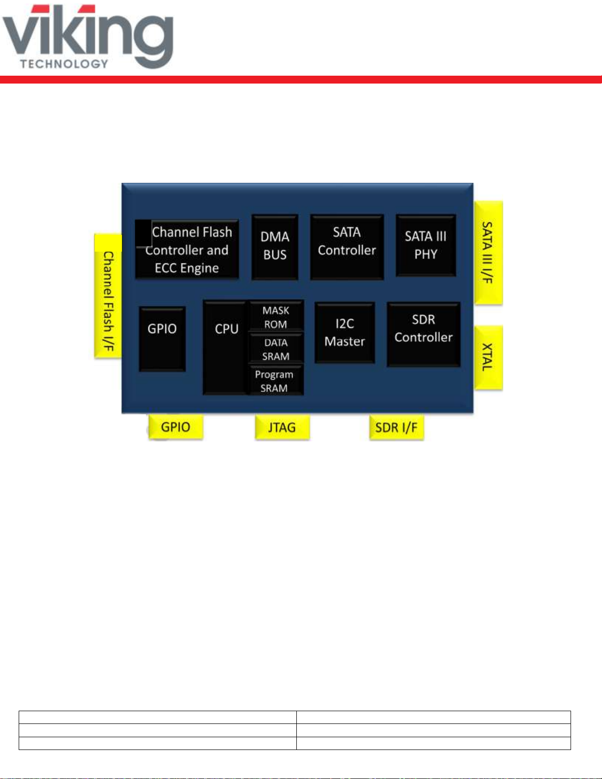
Figure 1-1: High-Level Block Diagram _____________________________________________ 10
Figure 3-1: Dimensions ________________________________________________________ 19
Figure 3-2: Dimension Details for M.2 42mm length __________________________________ 20
Figure 3-3: Dimension Details for M.2 card edge_____________________________________ 21
Figure 3-4: Dimension Details for M.2 connector and notch ____________________________ 22

Manual
7/24/2017
PSFEM6xxxxZxxx
Viking Technology
Revision C
Page 9 of 38
www.vikingtechnology.com
1 Introduction
Viking’s rugged industrial designed SSD’s offer the highest flash storage
reliability and performance in harsh environments such as shock, vibration,
humidity, altitude, ESD, and extreme temperatures.
1.1 Features
The SSD delivers the following features:
Offers seamless SATA Revision 3.0 interface support for SATA up to
6Gb/s
Low overall SSD power consumption
Supports Native Command Queuing (NCQ) to 32 commands
Compatible with all major SLC and MLC flash technologies
S.M.A.R.T.
Superior wear-leveling algorithm
Efficient error recovery

Manual
7/24/2017
PSFEM6xxxxZxxx
Viking Technology
Revision C
Page 10 of 38
www.vikingtechnology.com
1.2 Block Diagram
Figure 1-1: High-Level Block Diagram
Notes:
1.Support for up to 2-channels and 2 CE in the NAND Flash interface
2
2

Manual
7/24/2017
PSFEM6xxxxZxxx
Viking Technology
Revision C
Page 11 of 38
www.vikingtechnology.com
1.3 SATA Interface
The Serial ATA (SATA) interface is compliant with the SATA IO Serial
ATA specification, revision 3.0 that supports SATA up to 6 Gbps.
The SATA interface connects the host computer to the SSD subsystem.
The SATA interface runs at a maximum speed of 6 Gbps (Giga-bits per
second). If the host computer is unable to negotiate a speed of 6 Gbps,
the SATA interface automatically renegotiates to a speed of 3 Gbps or 1.5
Gbps.
For a list of supported commands and other specifics, please see Chapter 5.

Manual
7/24/2017
PSFEM6xxxxZxxx
Viking Technology
Revision C
Page 12 of 38
www.vikingtechnology.com
2 Product Specifications
2.1 Capacity and LBA count
Raw Capacity
(GB)
User Capacity
(GB)
LBA Count
8
8
15,649,200
16
14
27,370,224
16
16
31,277,232
32
30
58,626,288
32
32
62,533,296
64
60
117,231,408
64
64
125,045,424
128
120
234,441,648
128
128
250,069,680
256
240
468,862,128
256
256
500,118,192
Notes:
1. Per LBA1-03 spec, LBA counts = (97,696,368) + (1,953,504 * (Advertised Capacity in GBytes –50))

Manual
7/24/2017
PSFEM6xxxxZxxx
Viking Technology
Revision C
Page 13 of 38
www.vikingtechnology.com
2.2 Performance
Table 2-1: Maximum Sustained Read and Write Bandwidth
Capacity
Flash Structure
Performance
Power Consumption
CrystalDiskMark
ATTO
Read
Write
Read
Write
Read
Write
Devslp
(MB/s)
(MB/s)
(MB/s)
(MB/s)
(mW)
(mW)
(mW)
8GB
8GBx1, TSOP, TSB
15nm
320
105
560
540
830
765
4.9
16GB
16GBx1, TSOP, TSB
15nm
320
85
560
540
895
805
4.9
30/32GB
32GBx1, BGA, TSB
15nm
560
165
560
540
1,030
1,210
4.9
60/64GB
32GBx2, BGA, TSB
15nm
560
315
560
540
1,040
1,215
4.9
120/128GB
64GBx2, BGA, TSB
15nm
560
465
560
540
1,065
1,480
4.9
240/256GB
128GBx2, BGA, TSB
15nm
560
465
560
540
1,165
1,535
4.9
480/512GB
256GBx2, BGA, TSB
15nm
560
465
560
540
1,425
1,740
4.9
Notes:
1. Performance measured using CrystalDiskMark.
2. Performance may vary from flash configuration, SDR configuration, and platform.
3. Refer to Application Note AN0006 for Viking SSD Benchmarking Methodology.
4. Data is based on SSD’s using Toshiba A15nm Toggle NAND devices
5. L95A data not currently available
Table 2-2: Sequential Read and Write Bandwidth (Iometer 06)
Capacity
Flash Type
Read MB/s
(256K)
Write MB/s
(256K)
8GB
15nm
5371
3661
16GB
15nm
5371
3661
32GB
15nm
5371
3661
64GB
15nm
5371
3661
128GB
15nm
5371
3661
256GB
15nm
537
366
512GB
15nm
5371
3661
Notes:
1. Estimated Performance measured using Iometer 06 with queue depth set to 32.
2. Write Cache enabled with DDR cache.
3. Tested with VPFEM5256GZIAMTL (Toshiba MLC L die)
4.

Manual
7/24/2017
PSFEM6xxxxZxxx
Viking Technology
Revision C
Page 14 of 38
www.vikingtechnology.com
Table 2-3: Random Read/ Write Input/Output Operations per Second (IOPS)
(Iometer 06)
Capacity
Flash Type
Random Read
IOPS
(4K)
Random Write
IOPS
(4K)
8GB
15nm
142001
11001
16GB
15nm
142001
11001
32GB
15nm
142001
11001
64GB
15nm
142001
11001
128GB
15nm
142001
11001
256GB
15nm
14200
1100
512GB
15nm
142001
11001
Notes:
1. Estimated Performance measured using Iometer 06 with queue depth set to 32.
2. Write Cache enabled with DDR cache.
3. Tested with VPFEM5256GZIAMTL (Toshiba MLC L die)
4. Random IOPS cover the entire range of legal logical block addresses (LBA’s). Measurements are
performed on a full drive (all LBA’s have valid content).
5. Performance may vary by NAND type and host.
6. Refer to Application Note AN0006 for Viking SSD Benchmarking Methodology.
7. Data is based on SSD’s using Toshiba A15nm NAND devices
8. L95A data not currently available
2.3 Timing
Table 2-4: Timing Specifications
Type
Average Latency
Power-On-to-Ready (POR)
TBD
Command to DRQ
TBD
Time to Erase (ATA Secure Erase)
TBD
Notes:
1. Device measured using Drivemaster.
2. Sector Read/Write latency measured up to 2048 block transfers (512B/sector = 1 Block)
3. Queue depth set to 32 for NCQ
4. Sequential IOPS cover the entire range of legal logical block addresses (LBA’s). Measurements are
performed on a full drive (all LBA’s have valid content
5. DRQ (Data Transfer Requested) bit being asserted
2.3.1 STANDBY IMMEDIATE Command
The Power-On-to-Ready time assumes a proper shutdown (power removal
preceded by STANDBY IMMEDIATE command. A STANDBY IMMEDIATE
before power down always performs a graceful shutdown and does not require
the use of the hold-up circuit. Note that SMART attribute 174 "Unexpected Power
Loss" records the number of non-graceful power cycle events.

Manual
7/24/2017
PSFEM6xxxxZxxx
Viking Technology
Revision C
Page 15 of 38
www.vikingtechnology.com
Table 2-5: STANDBY IMMEDIATE Timing
Power Cycle Endurance
Min
Max
Unit
STANDBY IMMEDIATE to WE completed
-
72.9
Ms
Notes:
1.From Standby Immediate command to NAND Write Protect enable.
2.4 Electrical Characteristics
2.4.1 Absolute Maximum Ratings
Values shown are stress ratings only. Functional operation outside normal
operating values is not implied. Extended exposure to absolute maximum ratings
may affect reliability.
Table 2-6: Absolute Maximum Ratings
Description
Min
Max
Unit
Maximum Voltage Range for Vin
-0.2
6
V
Maximum Temperature Range
-40
85
C
2.4.2 Supply Voltage
The operating voltage is 3.3V
Table 2-7: Operating Voltage
Description
Min
Max
Unit
Operating Voltage for 3.3 V (+/- 5%)
3.135
3.465
V

Manual
7/24/2017
PSFEM6xxxxZxxx
Viking Technology
Revision C
Page 16 of 38
www.vikingtechnology.com
2.4.3 Supply Current
Table 2-8: Current Draw
Voltage
Mode
8GB
16GB
32GB
64GB
128GB
Unit
3.3V
Read (Average RMS)
N/A
N/A
325
235
395
mA
Writes (Average RMS)
N/A
N/A
300
250
305
mA
Idle
N/A
N/A
63
62
61
mA
Partial
N/A
N/A
11.5
11
11
mA
Slumber
N/A
N/A
6.7
6.4
6.9
mA
DEVSLP
N/A
N/A
0.98
0.98
0.98
mA
Notes:
1.Measured using 128GB MLC Toshiba A19nm NAND
2.4.4 Power Consumption
All onboard power requirements of the SSD are derived from the SATA 3.3V rail.
Table 2-9: Typical Power Consumption at 3.3V
Capacity
Flash
Structure
Flash Type
Read
Write
Partial
Slumber
Idle
DEVSLP
8GB
8GB x 1
TSOP, TSB
15nm
830
765
12.5
8
255
4.9
16GB
16GB x 1
TSOP, TSB
15nm
895
805
12.5
8
256
4.9
32GB
32GB x 1
TSOP, TSB
15nm
970
1,100
13
9
260
4.9
32GB
32GB x 1
BGA, TSB
15nm
1,030
1,210
12
7
255
4.9
64GB
32GB x 2
BGA, TSB
15nm
1,040
1,215
12
7
257
4.9
128GB
64GB x 2
BGA, TSB
15nm
1,065
1,480
12
7
255
4.9
256GB
128GB x2
BGA, TSB
15nm
1,165
1,535
12
7
260
4.9
512GB
256GB x2
BGA, TSB
15nm
1,425
1,740
14
10
260
4.9
Notes:
1.Units are mW
2.Measured using Toshiba A15 Toggle MLC NAND

Manual
7/24/2017
PSFEM6xxxxZxxx
Viking Technology
Revision C
Page 17 of 38
www.vikingtechnology.com
2.5 Environmental Conditions
2.5.1 Temperature and Altitude
Table 2-10: Temperature and Altitude Related Specifications
Conditions
Operating
Shipping
Storage
Commercial
Temperature- Ambient
0 to 70°C
-40 to 85°C
-40 to 85°C
Industrial
Temperature- Ambient
-40 to 85°C
-40 to 85°C
-40 to 85°C
Humidity (non-
condensing)
90% under 40C
93% under 40C
93% under 40C
2.5.2 Shock and Vibration
SSD products are tested in accordance with environmental specification for
shock and vibration
Table 2-11: Shock and Vibration Specifications
Stimulus
Description
Shock
500G, 2ms
Vibration
20 –80 Hz/1.52mm
80 –2000 Hz/20G
(X,Y,Z axis / 30 min for each)
2.5.3 Electromagnetic Immunity
M.2 is an embedded product for host systems and is designed not to impair with
system functionality or hinder system EMI/FCC compliance.

Manual
7/24/2017
PSFEM6xxxxZxxx
Viking Technology
Revision C
Page 18 of 38
www.vikingtechnology.com
2.6 Reliability
Table 2-12: Reliability Specifications
Parameter
Description
MTBF
Over 2,000,000 hours
ECC
72-bit per 1KByte
Read Endurance
Unlimited
Write Endurance
Capacity
TBW
8GB
12 TBW
16GB
23 TBW
32GB
45 TBW
64GB
90 TBW
128GB
181 TBW
256GB
262 TBW
512GB
544 TBW
Data retention
> 90 days at NAND expiration
NOTES:
1. Samples were built using Toshiba 15nm Toggle MLC NAND.
2. TBW may differ according to flash configuration and platform.
3. The endurance of SSD could be estimated based on user behavior, NAND endurance cycles,
and write amplification factor. It is not guaranteed by flash vendor

Manual
7/24/2017
PSFEM6xxxxZxxx
Viking Technology
Revision C
Page 19 of 38
www.vikingtechnology.com
3 Mechanical Information
3.1 Dimensions
Figure 3-1: Dimensions
d
Notes:
1. All dimensions are in millimeter. General tolerance is ± 0.15. PCB thickness 0.8 ± 0.08
2. Refer to Ordering Information table for the complete Viking part number that describes the “xxx”.
VRFEM6xxxNote2

Manual
7/24/2017
PSFEM6xxxxZxxx
Viking Technology
Revision C
Page 20 of 38
www.vikingtechnology.com
Figure 3-2: Dimension Details for M.2 42mm length
Notes:
1. All dimensions are in millimeter. General tolerance is ± 0.15. PCB thickness 0.8 ± 0.08
2. Refer to Ordering Information table for the complete Viking part number that describes the “xxx”.
VRFEM6xxxNote2
Table of contents
Other Viking Storage manuals