WA3RNC TR-35 User manual

1
TR-35 Lower Board Assembly Instructions 01/16/22
Refer to the above diagram while performing the following steps:
1) Install and solder relay RL1 to the board with the polarity bar toward the
board center. See the photo. Solder 10 pins.
2) Carefully form the leads of diode D5, if necessary, to fit on the board. The
banded end goes to the square pad. Position the diode fairly close to the
board. Solder and trim 2 leads.
3) Install and solder Polyfuse F1 to the board. Bend this part over as shown on
the overlay before soldering. Solder and trim 2 leads.
4) Install and solder the DC power jack J4. Make certain this jack is tight
against the board and is straight. Solder and trim 3 pins. These pins must be
trimmed after soldering to allow for proper fit into the case.
5) Install and solder the side-tone level 500-ohm pot R31 (marked 501). Solder
and trim 3 pins.

2
6) Install and solder PA bias pot R40 and low battery warning adjustment pot
R46. Both are 5k (marked 502). Solder and trim 6 pins.
7) Install Q18 BS170 TO-92 FET (marked with red). Place the flat side as shown
on the parts overlay. Position the part with about ¼” lead length above the
board. Solder and trim 3 leads.
8) Install Q6 FQN1N50C TO-92 FET (marked with blue). Place the flat side as
shown on the parts overlay. Position the part with about ¼” lead length
above the board. Solder and trim 3 leads.
9) Install and solder (6) 100uF electrolytic capacitors C49, C77, C78, C79, C80,
and C83. The longer positive leads goes to the square pad. All the
capacitors except C77 and C78 must be installed tight against the board.
Note that C77 and C78 must be installed lying down on the board. Bend the
leads BEFORE soldering. Solder and trim 12 leads.
10) Install and solder (2) 47uF electrolytic capacitors C53 and C91 tight against
the board. The longer lead goes to the square pad. Solder and trim 4 leads.
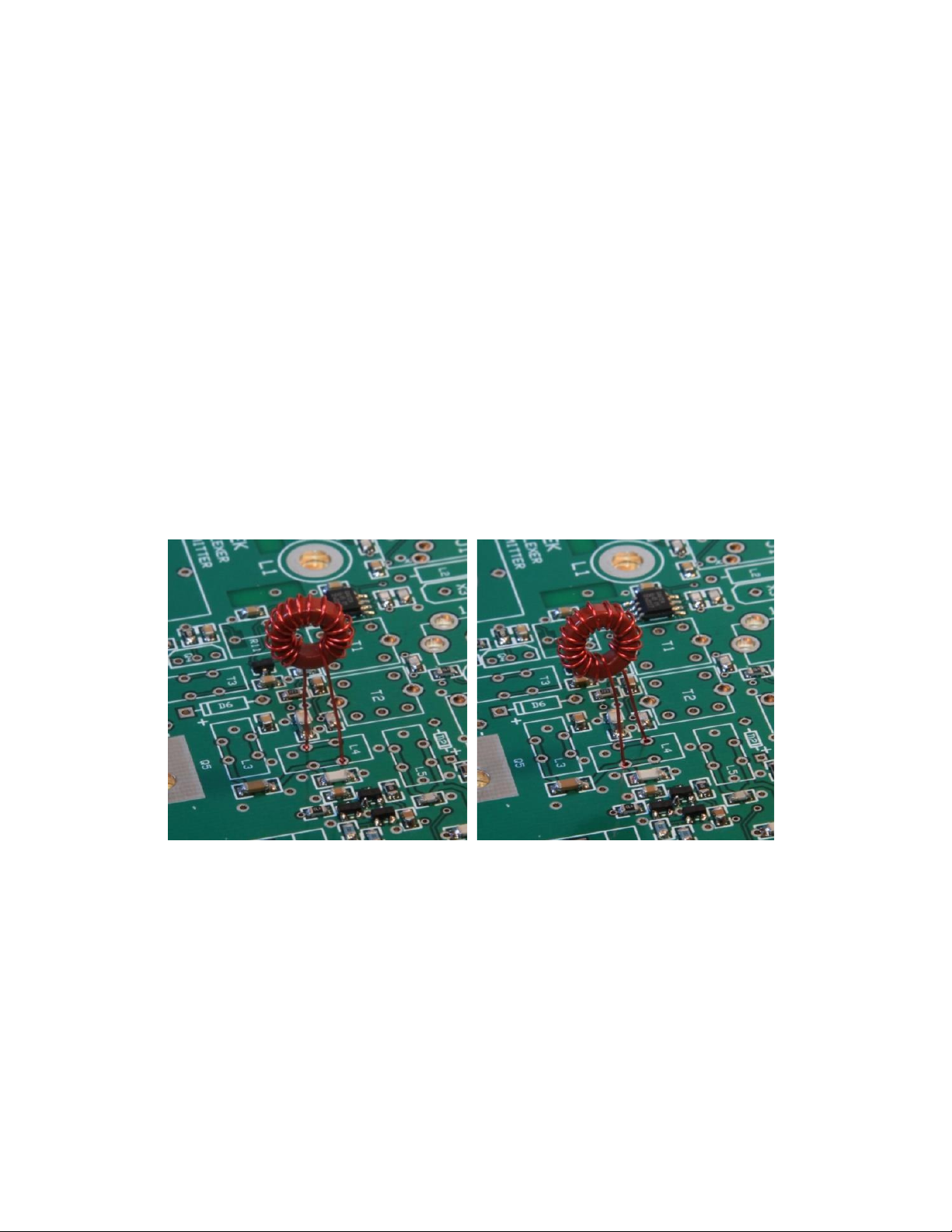
11) Form the leads of Q17, the final RF amplifier FET IRF510 so that the 3 leads
mate with the mounting holes while the tab hole mates with the FET
mounting hole through the heatsink. See the photo. Place the heatsink
against the board, with the clear mica washer between the heatsink and
the FET. Fit the FET leads into the mounting holes, and then insert the
mounting screw from the bottom through the board, heatsink, mica
washer, FET tab, and plastic insulator. Place the nut on top of the plastic
insulator. Make sure the plastic insulator fits inside the FET mounting hole.
Align the FET and heatsink with the mica washer between them. Tighten
the screw fairly tightly. Don’t deform or damage the plastic insulator. Use
an ohmmeter to check for shorts from the FET metal tab to ground. Solder
and trim 3 pins. Secure the nut to the screw with clear fingernail polish.

3
12) This step involves installation of 2 black ferrite toroidal inductors. The 3-
leaded toroid is installed at T2. The twisted 2-wire center lead goes to the
center hole, while the single wires go to the outside holes. The single red
and green wires can go into either outside hole (1 in each hole). The 2-
leaded 10-turn toroid is installed at L23. Mount the toroids vertically
against the board. Solder and trim 5 leads. Note that there are two sets of
holes for L17 through L23, and L26. Depending on how the coils were
wound, left hand or right hand, one pair of holes will make for a better fit.
Use either diagonal pair of holes, but be sure not to connect both coil leads
to pads that are connected together! See the Photo for examples of left-
and right-hand wound toroids. Neither is wrong, and either will work fine.
Note that turns on a toroidal core are always counted on the inside of the
core. Each time the wire goes through the center hole, it counts as a turn.
13) This step installs 3 yellow 10-turn toroids at L20, L21, and L22. Solder and
trim 6 leads.
14) Install the 2 red 12-turn toroids at L17 and L19. Solder and trim 4 leads.
15) This step installs 1 red and 1 yellow toroid, each with 11 turns. Install the
red one at L18, and the yellow one at L26. Solder and trim 4 leads.

4
16) Install the IF filter crystals X1 through X4. The crystals have been measured
and sorted, so they must be installed properly for maximum IF filter
effectiveness. The crystals are numbered according to the reference
designator where they will be installed. The crystal marked “1” will be
mounted at X1, and so on. The crystal leads need to be formed by carefully
bending them 90 degrees. See the photo.
Mount the crystals down tight against the board. Solder and trim 8 leads.
Ground the crystal cans with wires cut from the included sacrificial
resistors. Do not overheat the crystal cans! Be quick when soldering to the
cans. Trim the grounding wires. The resistors may be discarded.
17) The 16 pin connectors J1 and J2 will be installed together on both the
upper and lower boards. This step requires some attention. The male
connectors (.025” square pins) will be installed on the lower board (the one
with the heatsink), and the female connectors on the upper board (the one
with the OLED display). To allow for maximum pin engagement for these
connectors, the female connectors will not be assembled tight against the
upper board. There will be a small gap between the female connector body
and the bottom of the upper board. Start this step by installing the male
header pins into the top side of the board with the heat sink (lower board).
Make certain that these connectors are tight against the board. Solder one
pin on each connector and examine them for straightness before soldering
the rest of the pins. Once all 32 pins are soldered, locate the assembled top
board with the 12mm spacers attached, and place the board upside down
in front of you, with the spots for the upper board connectors J1 and J2
closest to you. Place the female 16 pin connectors into the bottom of the
upper board. Do not solder these connectors. Now carefully place the lower

5
board upside down over the upper board, carefully aligning the 4
connectors. The lower board mounting holes should line up with the
spacers mounted on the upper board. Once everything is lined up, carefully
press the boards together. Stop and investigate if something doesn’t seem
right, or if the board mounting holes do not line up. With the boards tight
together, locate the four 3mm x 6mm screws and use them to secure the
boards together. Turn the board set assembly right side up with the display
and controls facing up. Now, the object is to fully engage the female
connectors onto the lower board pins by pushing the female connectors
down onto the male pins as far as they will go. This may require the use a
flat surfaced object to gently push on the upper board connector pins to
fully seat them onto the lower board pins.
Note that this will let a small gap between the upper board surface and the
female connector. See the picture.
Note the gaps between the female connectors and the upper pc board
The upper board female connectors can now be soldered. Solder 32 pins.
18) Locate the 28-pin microcontroller IC U1. Observing antistatic measures,
carefully install U1 into the upper board 28 pin socket. Be sure to place the
pin 1 end toward the center of the board. Be careful not to bend any pins!
The orientation notch indicates pin 1 end.
This completes assembly of the upper and lower pc boards. Proceed to the
“Preliminary Checks and Tests” document.
Table of contents
Other WA3RNC Transceiver manuals