Wasco OPTOIO-PCIe32 ULTRA User manual

Handbuch
wasco®
wasco®
User‘s Guide
OPTOIO-PCIe32
ULTRA
EDP-No.: A-840810
32 optocoupler isolated digital inputs
32 optocoupler isolated digital outputs
32*32 -bit Counters
Timer
OC and IC Units
Board Identication
OPTOIO-PCIe32
ULTRA
EDV-Nr.: A-840810
32 Eingänge über Optokoppler
32 Ausgänge über Optokoppler
32*32 Bit Zähler
Timer
OC- und IC-Einheiten
Board-Identikation

2
OPTOIO-PCIe32ULTRA © 2019 by Messcomp Datentechnik GmbH DV02
2
OPTOIO-PCIe32ULTRA © 2019 by Messcomp Datentechnik GmbH EV02 22
wasco®wasco®
Copyright©2019 by Messcomp Datentechnik GmbH
Diese Dokumentation ist urheberrechtlich geschützt. Alle Rechte sind
vorbehalten.
Messcomp Datentechnik GmbH behält sich das Recht vor, die in dieser
DokumentationbeschriebenenProduktejederzeitundohneVorankündigung
zu verändern.
OhneschriftlicheGenehmigungderFirmaMesscompDatentechnikGmbH
darf diese Dokumentation in keinerlei Form vervielfältigt werden.
Geschützte Warenzeichen
BASICisteingeschütztesWarenzeichenvonDartmouthCollege.Windows
ist ein eingetragenes Warenzeichen von Microsoft.
wasco®ist ein eingetragenes Warenzeichen.
Haftungsbeschränkung
Die Firma Messcomp Datentechnik GmbH haftet für keinerlei durch
den Gebrauch der Interfacekarte OPTOIO-PCIe32ULTRA und dieser
Dokumentation direkt oder indirekt entstandene Schäden.
Copyright©2019 by Messcomp Datentechnik GmbH
This documentation is copyright by Messcomp Datentechnik GmbH. All
rights are reserved.
Messcomp Datentechnik GmbH reserves the right to modify the products
described in this manual at any time and without preannouncement.
No parts of this manual are allowed to be reproduced, copied, translated
or transmitted in any way without a prior written consent of Messcomp
Datentechnik GmbH.
Registered Trademarks
BASIC is a registered trademark of Dartmouth College.
Windows is a registered trademark of Microsoft.
wasco®is a registered trademark.
Disclaimer
The company Messcomp Datentechnik GmbH assumes no liability for
damages neither directly nor indirectly caused by the use of the interface
card OPTOIO-PCIe16ULTRA and this documentation.

3
OPTOIO-PCIe32ULTRA © 2019 by Messcomp Datentechnik GmbH DV02
3
OPTOIO-PCIe32ULTRA © 2019 by Messcomp Datentechnik GmbH EV02 33
wasco®wasco®
Table of Contents Inhaltsverzeichnis
1. Description........................................................................................5
2. Installation of the OPTOIO-PCIe32ULTRA...........................................6
2.1 Installation of the card into your system................................................................6
3. Connectors........................................................................................7
3.1 Position of the connector plugs on the board........................................................7
3.2 Pin assignment of CN1..........................................................................................8
3.3 Pin assignment of CN2..........................................................................................9
4. System Components......................................................................10
4.1 Block Diagram.....................................................................................................10
4.2 Access to the system components......................................................................11
5. 32 Optocoupler Isolated Digital Inputs.........................................12
5.1 Pin assignment of the input optocouplers............................................................12
5.2 Input voltage ranges............................................................................................13
5.3 Input wiring..........................................................................................................15
5.4 Input current ........................................................................................................15
5.5 Access to the inputs.............................................................................................16
5.6 Optocoupler inputs with digital lters...................................................................16
5.7 Interrupt functions of the optocoupler inputs .......................................................17
5.8 Port Addresses....................................................................................................21
6. 32 Optocoupler Outputs ................................................................25
6.1 Pin assignment of the output optocouplers .........................................................25
6.2 Optocoupler data.................................................................................................25
6.3 Output wiring .......................................................................................................25
6.4 Functions of the optocoupler outputs ..................................................................26
6.5 Port Addresses....................................................................................................27
7. Counter............................................................................................31
7.1 Basic function......................................................................................................31
7.2 Interrupt function..................................................................................................31
7.3 Port Addresses....................................................................................................32
8. Timer................................................................................................43
8.1 Using as an interval interrupt trigger....................................................................43
8.2 Port Addresses....................................................................................................44

4
OPTOIO-PCIe32ULTRA © 2019 by Messcomp Datentechnik GmbH DV02
4
OPTOIO-PCIe32ULTRA © 2019 by Messcomp Datentechnik GmbH EV02 44
wasco®wasco®
9. Input-Capture-Einheit 47
9.1 Kontinuierliche Messung periodischer Signale 47
9.2 Portadressen 49
10. Output-Compare-Einheit 53
10.1 PWM 53
10.2 Pulsausgabe 55
11. Interruptcontroller 61
11.1 Portadressen 63
12. Board-Identikation 75
12.1 Portadressen 76
13. Programmierung unter Windows®77
13.1 Installation des Windows®Treibers 77
13.2 Installation der Windows®Entwicklungsdateien 77
13.3 Programmierung der OPTOIO-PCIe32 mit wasco®-Treiber 80
13.4 Zugriff auf die Karte OPTOIO-PCIe32ULTRA 81
13.5 Zuordnung der Memory Mapped I/O-Adressen 81
13.6 Kompatibilität zur OPTOIO-PCI32STANDARD 82
14. Zubehör 83
14.1 Passendes wasco®-Zubehör 83
14.2 Anschlusstechnik (Anwendungsbeispiele) 83
14.3 Einzelkomponenten zur Eigenkonfektionierung 84
15. Fehlersuche 85
16. Technische Daten 86
17. Produkthaftungsgesetz 87
18. EG-Konformitätserklärung 89
9. Input Capture Unit..........................................................................47
9.1 Continuous measurement of periodic signals......................................................47
9.2 Port Addresses....................................................................................................49
10. Output Compare Unit...................................................................53
10.1 PWM..................................................................................................................53
10.2 Pulse output.......................................................................................................55
11. Interruptcontroller ........................................................................61
11.1 Port Addresses ..................................................................................................63
12. Board Identication......................................................................75
12.1 Port Addresses..................................................................................................76
13. Programming under Windows®...................................................77
13.1 Installation of the Windows®driver....................................................................77
13.2 Installation of the Windows® development les .................................................77
13.3 Programming the OPTOIO-PCIe32 with wasco®driver.....................................80
13.4 Access to the OPTOIO-PCIe32ULTRA ..................................................................81
13.5 Assignment of the Memory Mapped I/O Addresses ..........................................81
13.6 Compatibility to OPTOIO-PCI32STANDARD.............................................................82
14. Accessories ..................................................................................83
14.1 Matching wasco®accessories...........................................................................83
14.2 Connection Technique (application examples)..................................................83
14.3 Single components for customized assembly ...................................................84
15. Troubleshooting ...........................................................................85
16. Specications ...............................................................................86
17. Product Liability Act.....................................................................87
18. CE Conrmation ...........................................................................89

5
OPTOIO-PCIe32ULTRA © 2019 by Messcomp Datentechnik GmbH DV02
5
OPTOIO-PCIe32ULTRA © 2019 by Messcomp Datentechnik GmbH EV02 55
wasco®wasco®
1. Description 1. Produktbeschreibung
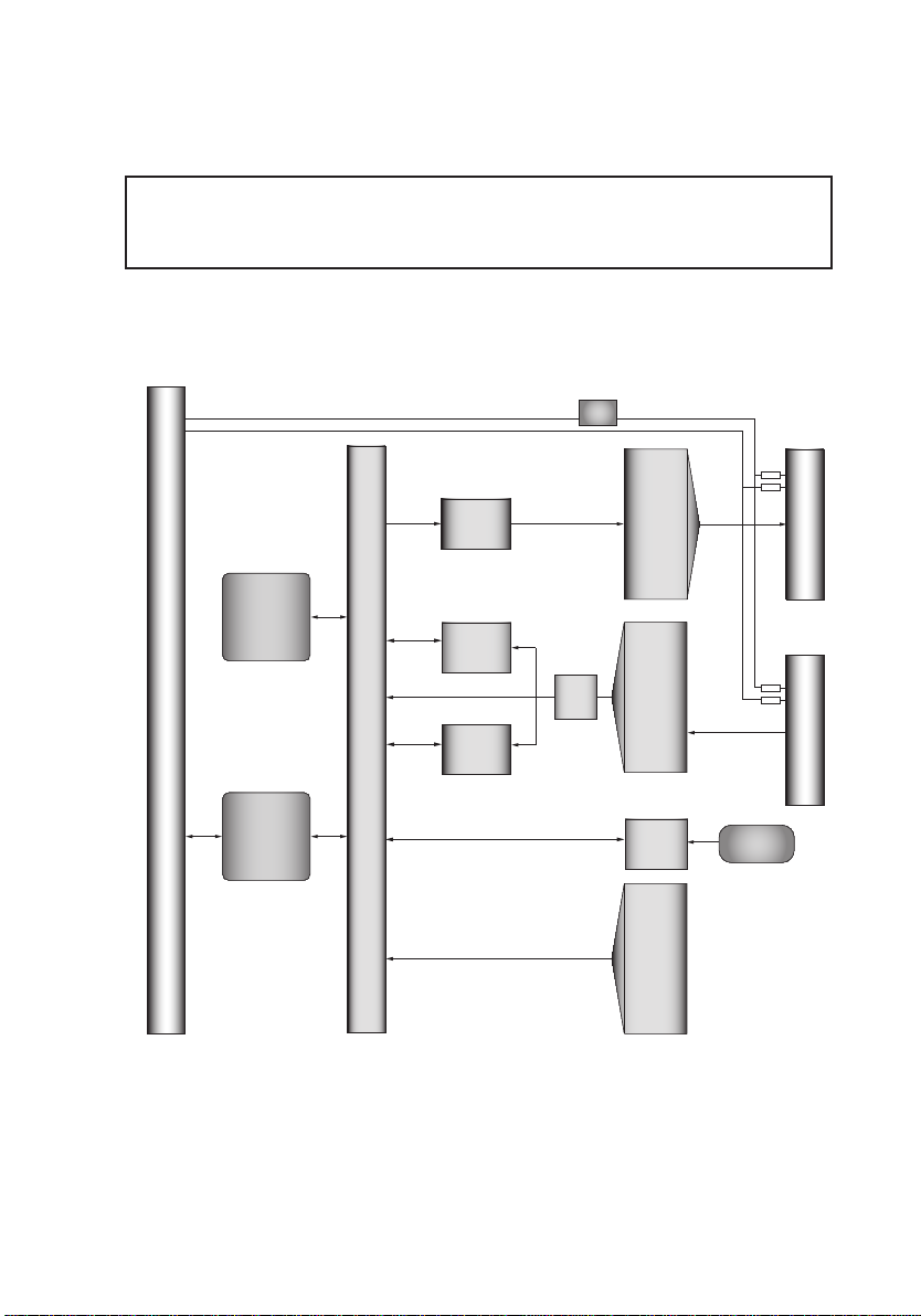
Die OPTOIO-PCIe32ULTRA (Boardname: WASCO-PCIe8132) bietet 32
digitale Eingänge und 32 digitale Ausgänge mit galvanischer Trennung
für jeden einzelnen Kanal. Die Potentialtrennung gewährleisten bei den
Ein- wie Ausgängen hochwertige Optokoppler. Spezielle, leistungsfähige
Ausgangsoptokoppler bewältigen einen Schaltstrom von bis zu 150 mA.
JederEin-undAusgangistzusätzlichdurchSchutzdiodengegenschädliche
Spannungsspitzen und Impulse geschützt. Über Jumperblöcke sind zwei
verschiedene Eingangs-Spannungsbereiche einstellbar. Jedem Eingang
kanneinprogrammierbarerFilterzugeordnetwerden,umEingangsimpulse
unter einer einstellbaren Impulsdauer auszublenden.
Neben den galvanisch getrennten I/Os stehen mehrere Zähler, Output-
Compare-Einheiten (z.B. PWM) und Input-Capture-Einheiten (z.B.
Periodenmessung) zur Verfügung. Interruptauslösungen sind durch alle
Optokopplereingänge, Zähler und IC-Einheiten sowie zeitabhängig durch
zwei32-Bit-Timermöglich.DieAnschlüssederAusgangsoptokoppler sind
der am Slotblech der Platine montierten 68poligen SCSI-Buchse zuge-
führt. Die Optokoppler-Eingänge liegen am 68poligen SCSI-Stecker auf
der Platine an. Über ein als Option erhältliches Steckerverlegungs-Set ist
die Verlegung auf eine 68polige D-Sub-Buchse mit Slotblech möglich.
Die Steckerbelegung ist bezüglich der Optokoppler-Ein/Ausgänge iden-
tisch zu den PCI-Karten OPTOIO-PCI32, ein Umstieg auf PCIe32ULTRA ist
dadurch einfach realisierbar.
Des Weiteren besitzt die Karte einen Board-Identikations-Jumperblock,
um mehrere identische Karten im PC unterscheiden zu können.
OPTOIO-PCIe32ULTRA (boardname:WASCO-PCIe8132)provides32digital
inputs and 32 digital outputs, every single channel is galvanically isolated
by optocouplers of high quality. Special, high-power output optocouplers
handle a switching current of up to 150 mA. Each input or output is pro-
tected from harmful voltage peaks and pulses by additional protection
diodes. You easily can adjust two different input voltage ranges by setting
jumpers. A programmable lter can be assigned to each input channel to
hide input pulses below an adjustable pulse duration.
In addition to the galvanically isolated inputs and outputs several coun-
ters are available as well as Output Compare units (e.g. PWM) and Input
Capture units (e.g. for period measurement).All optocoupler inputs, coun-
ters, IC units and the two 32-bit timers (time-dependent) can initiate an
interrupt. The output optocouplers are connected to a 68-pin SCSI female
jack mounted on the board‘s slot bracket. The optocoupler inputs are
connected to a 68-pin onboard SCSI plug. As an option a special plug-in
cable set is available, to relocate the connection to a 68-pin Sub-D jack
with slot brackets.
The pin assignment as of the optocoupler inputs and outputs is identical
to the PCI cards OPTOIO-PCI32. Therefore a switch to PCIe32ULTRA is
easy to implement.
Furthermore, the card provides a jumper block for card identication in
order to distinguish several identical cards in your system.

6
OPTOIO-PCIe32ULTRA © 2019 by Messcomp Datentechnik GmbH DV02
6
OPTOIO-PCIe32ULTRA © 2019 by Messcomp Datentechnik GmbH EV02 66
wasco®wasco®
2. Installation of the OPTOIO-PCIe32ULTRA 2. Installation der OPTOIO-PCIe32ULTRA
2.1 Installation der Karte in den Rechner
Achten Sie vor dem Einbau der OPTOIO-PCIe32 darauf, dass der Rech-
ner vom Netz getrennt oder zumindest ausgeschaltet ist. Beim Einbau
der Interface-Karte in den laufenden Rechner besteht die Gefahr, dass
neben der OPTOIO-PCIe32 auch andere Karten des PCs oder Rechners
beschädigt oder zerstört werden.
Wählen Sie in Ihrem Rechner einen freien PCIe-Steckplatz in den Sie
dann die Karte einsetzen. Nehmen Sie dazu auch das Benutzerhandbuch
Ihres Computers zu Hilfe. Verschrauben Sie das Slotblech der Platine mit
dem Rechnergehäuse, damit sich die Karte nicht während des Betriebs
unter Einwirkung der Anschlusskabel aus dem Steckplatz lösen kann.
2.1 Installation of the card into your system
Before you insert the OPTOIO-PCIe32 unplug the power cord or make
sure, there is no current to/in the computer. Inserting the interface card in
a running system may cause damaging or destroying not only the OPTO-
IO-PCIe16ULTRA, but even other already inserted cards of your computer.
Select an empty PCIe slot of your computer for then inserting the card.
Please refer to the computer‘s manual for support. Secure the circuit
board by screwing the slot bracket to the casing of the computer to avoid
a card‘s loosening by effects of the connecting cables.

7
OPTOIO-PCIe32ULTRA © 2019 by Messcomp Datentechnik GmbH DV02
7
OPTOIO-PCIe32ULTRA © 2019 by Messcomp Datentechnik GmbH EV02 77
wasco®wasco®
3. Connectors
3.1 Position of the connector plugs on the board
CN1: Optocoupler Outputs OUT00...OUT31
CN2: Optocoupler Inputs IN00...IN31
CN1 CN2
3. Anschlussstecker
3.1 Lage der Anschlussstecker auf der Platine
CN1: Optokoppler-Ausgänge OUT00...OUT31
CN2: Optokoppler-Eingänge IN00...IN31
CN1 CN2

8
OPTOIO-PCIe32ULTRA © 2019 by Messcomp Datentechnik GmbH DV02
8
OPTOIO-PCIe32ULTRA © 2019 by Messcomp Datentechnik GmbH EV02 88
wasco®wasco®
3.2 Steckerbelegung von CN1
Vcc:
Interne Versorgungsspannung (+ 5V) der PCIe-Karte (nur durch Einlöten einer Drahtbrücke
an B11). Hier niemals eine externe Spannung anlegen.
GND:
Masse des Rechners (nur durch Einlöten einer Drahtbrücke an B12)
3.2 Pin assignment of CN1
Vcc:
Internal voltage supply (+ 5V) (a wiring bridge must be soldered to B11). Never apply an
external voltage across this pin.
GND:
Ground connection (only when a wiring bridge is soldered to B12).
GND
GND
OUT31-
OUT30-
OUT29-
OUT28-
OUT27-
OUT26-
OUT25-
OUT24-
OUT23-
OUT22-
OUT21-
OUT20-
OUT19-
OUT18-
OUT17-
OUT16-
OUT15-
OUT14-
OUT13-
OUT12-
OUT11-
OUT10-
OUT09-
OUT08-
OUT07-
OUT06-
OUT05-
OUT04-
OUT03-
OUT02-
OUT01-
OUT00-
Vcc
Vcc
OUT31+
OUT30+
OUT29+
OUT28+
OUT27+
OUT26+
OUT25+
OUT24+
OUT23+
OUT22+
OUT21+
OUT20+
OUT19+
OUT18+
OUT17+
OUT16+
OUT15+
OUT14+
OUT13+
OUT12+
OUT11+
OUT10+
OUT09+
OUT08+
OUT07+
OUT06+
OUT05+
OUT04+
OUT03+
OUT02+
OUT01+
OUT00+
68 34
67 33
66 32
65 31
64 30
63 29
62 28
61 27
60 26
59 25
58 24
57 23
56 22
55 21
54 20
53 19
52 18
51 17
50 16
49 15
48 14
47 13
46 12
45 11
44 10
43 9
42 8
41 7
40 6
39 5
38 4
37 3
36 2
35 1
GND
GND
OUT31-
OUT30-
OUT29-
OUT28-
OUT27-
OUT26-
OUT25-
OUT24-
OUT23-
OUT22-
OUT21-
OUT20-
OUT19-
OUT18-
OUT17-
OUT16-
OUT15-
OUT14-
OUT13-
OUT12-
OUT11-
OUT10-
OUT09-
OUT08-
OUT07-
OUT06-
OUT05-
OUT04-
OUT03-
OUT02-
OUT01-
OUT00-
Vcc
Vcc
OUT31+
OUT30+
OUT29+
OUT28+
OUT27+
OUT26+
OUT25+
OUT24+
OUT23+
OUT22+
OUT21+
OUT20+
OUT19+
OUT18+
OUT17+
OUT16+
OUT15+
OUT14+
OUT13+
OUT12+
OUT11+
OUT10+
OUT09+
OUT08+
OUT07+
OUT06+
OUT05+
OUT04+
OUT03+
OUT02+
OUT01+
OUT00+
68 34
67 33
66 32
65 31
64 30
63 29
62 28
61 27
60 26
59 25
58 24
57 23
56 22
55 21
54 20
53 19
52 18
51 17
50 16
49 15
48 14
47 13
46 12
45 11
44 10
43 9
42 8
41 7
40 6
39 5
38 4
37 3
36 2
35 1

9
OPTOIO-PCIe32ULTRA © 2019 by Messcomp Datentechnik GmbH DV02
9
OPTOIO-PCIe32ULTRA © 2019 by Messcomp Datentechnik GmbH EV02 99
wasco®wasco®
3.3 Steckerbelegung von CN23.3 Pin assignment of CN2
Vcc:
Internal voltage supply (+ 5V) (a wiring bridge must be soldered to B21). Never apply an
external voltage across this pin.
GND:
Ground connection (only when a wiring bridge is soldered to B22).
GND
GND
IN31-
IN30-
IN29-
IN28-
IN27-
IN26-
IN25-
IN24-
IN23-
IN22-
IN21-
IN20-
IN19-
IN18-
IN17-
IN16-
IN15-
IN14-
IN13-
IN12-
IN11-
IN10-
IN09-
IN08-
IN07-
IN06-
IN05-
IN04-
IN03-
IN02-
IN01-
IN00-
Vcc
Vcc
IN31+
IN30+
IN29+
IN28+
IN27+
IN26+
IN25+
IN24+
IN23+
IN22+
IN21+
IN20+
IN19+
IN18+
IN17+
IN16+
IN15+
IN14+
IN13+
IN12+
IN11+
IN10+
IN09+
IN08+
IN07+
IN06+
IN05+
IN04+
IN03+
IN02+
IN01+
IN00+
68 34
67 33
66 32
65 31
64 30
63 29
62 28
61 27
60 26
59 25
58 24
57 23
56 22
55 21
54 20
53 19
52 18
51 17
50 16
49 15
48 14
47 13
46 12
45 11
44 10
43 9
42 8
41 7
40 6
39 5
38 4
37 3
36 2
35 1
Vcc:
Interne Versorgungsspannung (+ 5V) der PCIe-Karte (nur durch Einlöten einer Drahtbrücke
an B21). Hier niemals eine externe Spannung anlegen.
GND:
Masse des Rechners (nur durch Einlöten einer Drahtbrücke an B22)
GND
GND
IN31-
IN30-
IN29-
IN28-
IN27-
IN26-
IN25-
IN24-
IN23-
IN22-
IN21-
IN20-
IN19-
IN18-
IN17-
IN16-
IN15-
IN14-
IN13-
IN12-
IN11-
IN10-
IN09-
IN08-
IN07-
IN06-
IN05-
IN04-
IN03-
IN02-
IN01-
IN00-
Vcc
Vcc
IN31+
IN30+
IN29+
IN28+
IN27+
IN26+
IN25+
IN24+
IN23+
IN22+
IN21+
IN20+
IN19+
IN18+
IN17+
IN16+
IN15+
IN14+
IN13+
IN12+
IN11+
IN10+
IN09+
IN08+
IN07+
IN06+
IN05+
IN04+
IN03+
IN02+
IN01+
IN00+
68 34
67 33
66 32
65 31
64 30
63 29
62 28
61 27
60 26
59 25
58 24
57 23
56 22
55 21
54 20
53 19
52 18
51 17
50 16
49 15
48 14
47 13
46 12
45 11
44 10
43 9
42 8
41 7
40 6
39 5
38 4
37 3
36 2
35 1

10
OPTOIO-PCIe32ULTRA © 2019 by Messcomp Datentechnik GmbH DV02
10
OPTOIO-PCIe32ULTRA © 2019 by Messcomp Datentechnik GmbH EV02 1010
wasco®wasco®
4.1 Blockschaltbild
4. Systemkomponenten
4.1 Block Diagram
4. System Components
PCIe x1
PCIe Bus
Interface
Control
and
Interrupt
Logic
+12V
32-bit
Internal Data Bus
+12V 5V
GND
68-pin SCSI socket 68-pin SCSI socket
Optocoupler Inputs
IN00...IN31 Optocoupler Outputs
OUT00...OUT31
Board Identification
2* OC
Unit
32* Counters
2* IC
Unit
Quartz
2* 32-bit
Timer
Filter
PCIe x1
PCIe Bus
Interface
Steuer-
und
Interrupt
Logik
+12V
32 Bit interner Datenbus
+12V 5V
GND
68polige SCSI-Buchse 68polige SCSI-Buchse
Optokopplereingänge
IN00...IN31 Optokopplerausgänge
OUT00...OUT31
Board Identifikation
2* OC-
Einheit
32* Zähler
2* IC-
Einheit
Quarz
2* 32 Bit
Timer
Filter

11
OPTOIO-PCIe32ULTRA © 2019 by Messcomp Datentechnik GmbH DV02
11
OPTOIO-PCIe32ULTRA © 2019 by Messcomp Datentechnik GmbH EV02 1111
wasco®wasco®
PCIe Bus
Interface
Control
Logic
32 Bit PCIe Connector
32 Bit
internal
Data Bus
Fig 4.2
4.2 Zugriff auf die Systemkomponenten
Der Zugriff auf die Hardware-Komponenten der OPTOIO-PCIe32 erfolgt
durch das Lesen von bzw. Schreiben in Memory-Mapped I/O-Adressen
mit Hilfe von Library-Funktionen. Die für die OPTOIO-PCIe32 relevanten
Adressen ergeben sich abhängig von einer vom BIOS vergebenen
Basisadresse.DerZugriffaufdieOPTOIO-PCIe32erfolgtausschließlichim
Doppel-Wort-Zugriff (Hinweise hierzu nden Sie im Kapitel Programmierung
sowie in den Beispielprogrammen auf der mitgelieferten CD).
PCIe Bus
Interface Steuer-
Logik
32 Bit PCIe Connector
32 Bit
interner
Datenbus
Abb. 4.2
4.2 Access to the system components
You can access to the hardware components of the OPTOIO-PCIe32 by
readingfromorwritingtoMemoryMappedI/Oaddressesusinglibraryfunc-
tions. The addresses relevant to the OPTOIO-PCIe32 arise depending on
theBIOSassignedbaseaddress.AccesstotheOPTOIO-PCIe32isexclu-
sively in double-word access (you will nd more information in the chapter
Programming as well as in the sample programs on the supplied CD)

12
OPTOIO-PCIe32ULTRA © 2019 by Messcomp Datentechnik GmbH DV02
12
OPTOIO-PCIe32ULTRA © 2019 by Messcomp Datentechnik GmbH EV02 1212
wasco®wasco®
TheOPTOIO-PCIe32provides32inputchannels,eachofwhichisoptically
isolated by optocouplers. The isolation voltage between GND and input is
500 VDC. The voltage within the input channels is limited to 50 VDC.
5.1 Pin assignment of the input optocouplers
5. 32 Optocoupler Isolated Digital Inputs
16,14,12,10 15,13,11,9
1,3,5,7 2,4,6,8
Fig. 5.1
Die OPTOIO-PCIe32 verfügt über 32 Eingangskanäle, deren galvanische
Trennung mittels Optokoppler erreicht wird. Die Isolationsspannung zwi-
schen Masse des Computers und Eingang beträgt 500 Volt, während die
Spannung zwischen den Eingangskanälen auf 50 Volt begrenzt ist.
5.1 Pinbelegung der Eingangsoptokoppler
5. 32 Optokopplereingänge
16,14,12,10 15,13,11,9
1,3,5,7 2,4,6,8
Abb. 5.1

13
OPTOIO-PCIe32ULTRA © 2019 by Messcomp Datentechnik GmbH DV02
13
OPTOIO-PCIe32ULTRA © 2019 by Messcomp Datentechnik GmbH EV02 1313
wasco®wasco®
5.2 Input voltage ranges
You can choose between two different input voltage ranges for each opto-
coupler input by setting jumpers on the blocks JP3, JP4, JP5 and JP6.
Fig. 5.2
JP5 JP6
JP3 JP4
5.2 Eingangsspannungsbereiche
Durch das Setzen von Jumpern auf den Blöcken JP3, JP4, JP5 und JP6
kann für jeden Optokopplereingang zwischen zwei Eingangsspannungs-
bereichen gewählt werden.
Abb. 5.2
JP5 JP6
JP3 JP4

14
OPTOIO-PCIe32ULTRA © 2019 by Messcomp Datentechnik GmbH DV02
14
OPTOIO-PCIe32ULTRA © 2019 by Messcomp Datentechnik GmbH EV02 1414
wasco®wasco®
1 2
3 4
5 6
7 8
IN00
IN01
IN02
IN03
9 10
IN04
IN05
IN06
IN07
11 12
13
15
14
16
1 2
3 4
5 6
7 8
IN08
IN09
IN10
IN11
JP4
9 10
IN12
IN13
IN14
IN15
11 12
13
15
14
16
1 2
3 4
5 6
7 8
IN16
IN17
IN18
IN19
9 10
IN20
IN21
IN22
IN23
11 12
13
15
14
16
1 2
3 4
5 6
7 8
IN24
IN25
IN26
IN27
JP6
9 10
IN28
IN29
IN30
IN31
11 12
13
15
14
16
JP3 JP5
Die Daten der zwei Eingangsspannungsbereiche entnehmen Sie bitte der
folgenden Tabelle:
Jumper LOW HIGH
gesetzt 0...1 V 5...15 V
nicht gesetzt 0...2 V 14...30 V
Beispiel:
Durch das Setzen eines Jumpers zwischen Pin1 und Pin2 des Jumper-
blocks JP3 wechselt der Eingangsspannungsbereich des IN00 von 0..2V
(Low) und 14..30V (High) auf 0..1V (Low) und 5..15V (High). Die rest-
lichen Eingangsspannungsbereiche bleiben unverändert.
1 2
3 4
5 6
7 8
IN00
IN01
IN02
IN03
9 10
IN04
IN05
IN06
IN07
11 12
13
15
14
16
1 2
3 4
5 6
7 8
IN08
IN09
IN10
IN11
JP4
9 10
IN12
IN13
IN14
IN15
11 12
13
15
14
16
1 2
3 4
5 6
7 8
IN16
IN17
IN18
IN19
9 10
IN20
IN21
IN22
IN23
11 12
13
15
14
16
1 2
3 4
5 6
7 8
IN24
IN25
IN26
IN27
JP6
9 10
IN28
IN29
IN30
IN31
11 12
13
15
14
16
JP3 JP5
Example:
By placing a jumper over Pin1 and Pin2 of the jumper block JP3 the input
voltage range of IN00 changes from 0..2V (Low) and 14..30V (High) to
0..1V (Low) and 5..15V (High). The remaining input voltage ranges keep
unaffected.
For the data of the two input voltage ranges, please refer to the following
table:
Jumper LOW HIGH
closed 0...1 V 5...15 V
open 0...2 V 14...30 V

15
OPTOIO-PCIe32ULTRA © 2019 by Messcomp Datentechnik GmbH DV02
15
OPTOIO-PCIe32ULTRA © 2019 by Messcomp Datentechnik GmbH EV02 1515
wasco®wasco®
UE- 1,1V
3400Ω
IE ≈
UE- 1,1V
1000Ω
IE ≈
5.3 Eingangsbeschaltung
5.4 Eingangsstrom
UE- 1,1V
3400Ω
IE ≈ (Jumper nicht gesetzt)
UE- 1,1V
1000Ω
IE ≈ (Jumper gesetzt)
Optokoppler
Jumper
IN.. +
IN.. -
1K 2K4
UESchutzdiode
Abb. 5.3
5.3 Input wiring
5.4 Input current
(Jumper open)
(Jumper closed)
Fig 5.3
Optocoupler
Jumper
IN.. +
IN.. -
1K 2K4
UEProtection
Diode

16
OPTOIO-PCIe32ULTRA © 2019 by Messcomp Datentechnik GmbH DV02
16
OPTOIO-PCIe32ULTRA © 2019 by Messcomp Datentechnik GmbH EV02 1616
wasco®wasco®
OPTOIN(0)
IC-Einheit
Filter
0-65535μs OPTOIN-Interrupts(0)
a b
IN00
1 3 5 7 9 11 13
a
b
μs
5.5 Zugriff auf die Eingänge
UmdenZustandderOptokopplereingängezuermitteln,mussdasRegister
OPTOIN ausgelesen werden. Jedes Bit des 32bit-Wertes steht für jeweils
einen Eingang wie aus der Registertabelle zu entnehmen.
Anwendungsbeispiel
AlsBeispielwird jederdritteOptokopplereingangdes Eingangssteckers
auf HIGH und der Rest auf LOW gelegt. Wird das Register OPTOIN
gelesen, so liefert die Karte den Wert 0x44444444(hex) zurück. Aus
diesem Wert können nun die Zustände der einzelnen Eingänge durch
eine Und-Verknüpfung herausgeltert werden.
5.6 Optokopplereingänge mit digitalem Filter
Jeder Optokopplereingang des Boards WASCO-PCIe8132 besitzt
einen eigenen konfigurierbaren digitalen Filter, um Störungen oder
Einschwingungen des Eingangssignals zu ltern. Dabei überprüft der
Filter wie in Abb. 5.5 gezeigt, ob ein anliegendes Signal lange genug
anliegt. Ist dies nicht der Fall, so wird z.B. ein zu kurzer Puls ignoriert. Die
Mindestzeit,welcheeineSignaländerungamjeweiligenEinganganliegen
muss, um nicht geltert zu werden, wird über das Register OPTOINFILx
eingestellt. Hier kann eine Filterbreite von 0 - 65535µs in 1-µs-Schritten
eingestellt werden. Im Default-Zustand ist der Filter deaktiviert, sprich die
Filterdauer beträgt 0µs.
OPTOIN(0)
IC-Einheit
Filter
0-65535μs OPTOIN-Interrupts(0)
a b
IN00
1 3 5 7 9 11 13
a
b
μs
Abb. 5.4 Abb. 5.5
5.5 Access to the inputs
In order to determine the state of the optocoupler inputs, the register
OPTOIN has to be read out. Every bit of the 32-bit value stands for one
input as shown in the register table.
Application example:
As an example every third optocoupler input of the input plug shall be
set to HIGH and all the rest to LOW. When the register OPTOIN is read,
the card returns the value 0x44444444(hex). Out of this value you can
lter the states of every single input by an AND-link operation.
5.6 Optocoupler inputs with digital lters
Each of the optocoupler inputs of the board WASCO-PCIe8132 has its
own congurable digital lter to lter spurious pulses and transients of the
input signal.
For that the lter checks whether or not a signal is applied long enough,
as shown in g. 5.5. If this is not the case, a too short pulse for example
will be ignored. In register OPTOINFILx you can adjust the minimum time
of how long the signal has to be applied to be considered. You can adjust
a lter width of 0 - 65535µs in steps of 1µs.
In state of default the lter is deactivated, say the lter duration is 0 µs.
Fig. 5.4 Fig. 5.5

17
OPTOIO-PCIe32ULTRA © 2019 by Messcomp Datentechnik GmbH DV02
17
OPTOIO-PCIe32ULTRA © 2019 by Messcomp Datentechnik GmbH EV02 1717
wasco®wasco®
Zubeachtenist beiderVerwendungderFilter,dassdieOptokopplereingänge
zum einen weit längere Schaltzeiten über 1µs besitzen und zum anderen
unterschiedlichsteileSteigungs- undFallkurvenaufweisen.Diesewerden
bei der Filterkonguration aufgrund von Bauteiltoleranzen unter den
Optokopplern nicht berücksichtigt und müssen vom Anwender selbst mit
einberechnet werden. Werden diese Schaltzeiten nicht mit einberechnet,
kann dies dazu führen, dass Signale am Optokopplereingang geltert
werden, obwohl sie theoretisch lange genug anliegen.
5.7 Interruptfunktionen der Optokopplereingänge
Um Änderungen an den Optokopplereingängen ohne regelmä-
ßiges Abfragen der Eingänge durch den PC zu erkennen, bietet die
OPTOIO-PCIe32 mehrereInterruptmöglichkeitenan.Sogibteszumeinen
die Möglichkeit, dass die Karte bei einer steigenden Flanke an einem
der Eingänge einen Interrupt am PC auslöst, oder zum anderen, dass
sie dem PC durch einen Interrupt eine generelle Änderung der Eingänge
signalisiert.
Neben diesem Kapitel lesen Sie bitte das Kapitel Interruptcontroller
durch.
Using the lters please note that the optocoupler inputs on one hand have
response times much longer than 1µs and on the other hand may vary in
steepness of rising and falling curves. This is not considered at the lter
conguration, as the optocouplers may show varying component tolerances.
The user has to allow for this by himself. Not considerung these switching
times may lead to a ltering out of signals at the optocoupler input, even
though theoretically they are applied long enough.
5.7 Interrupt functions of the optocoupler inputs
Todetectchangestotheoptocouplerinputswithoutperiodicallyqueryingthe
input state via PC, the OPTOIO-PCIe32 offers several interrupt options.
On one hand the card is aible to trigger an interrupt on one of the inputs on
a rising edge. On the other hand the card can signal to the PC a general
change of the input states by an interrupt.
For further information please see the chapter Interrupt Controller.

18
OPTOIO-PCIe32ULTRA © 2019 by Messcomp Datentechnik GmbH DV02
18
OPTOIO-PCIe32ULTRA © 2019 by Messcomp Datentechnik GmbH EV02 1818
wasco®wasco®
5.7.1 Flankenerkennung
Um steigende Flanken an den Optokopplereingängen zu erkennen,
besitzt jeder einzelne Eingang eine Flankenerkennung mit zuschaltbarer
Interruptfunktion. Dafür wird ein 32bit Interruptregister (OPTOINIF) bereit-
gestellt, welches für jeden Eingangskanal ein Bit zur Flankenerkennung
zur Verfügung stellt. Sobald an einem Eingang eine steigende Flanke
durch die Karte erkannt wird, wird das jeweilige Bit im Register OPTOINIF
gesetzt. Ist mindestens eines der freigeschalteten Bits gesetzt, wird dies
über eine Leitung an den Interruptcontroller weitergeleitet.
Das Freischalten der Interruptfunktion erfolgt durch das Beschreiben
des 32bit Registers OPTOINFe. Dabei repräsentiert jedes einzelne Bit
einen Eingang. Wie aus der Tabelle Portadressen (Kapitel 11.1) zu ent-
nehmen ist, bedeutet eine 1 im jeweiligen Bit eine Aktivierung und eine
0 eine Deaktivierung der Interruptfunktion. Steht im Bit also z.B. eine 0,
so wird bei einer steigenden Flanke im Register OPTOINIF zwar das ent-
sprechende Bit gesetzt, jedoch wird dieses Bit bei der Interruptauslösung
nicht berücksichtigt.
Im Defaultzustand sind alle Interruptkanäle deaktiviert.
Nach dem ausgelösten Interrupt muss in der entsprechenden Interrupt-
Service-Routine durch das Einlesen des Registers OPTOINIF die Quelle
ermittelt und anschließend das Bit gelöscht werden, indem das zum
Quellenkanal gehörige Bit im Register OPTOINFr gesetzt wird. Nachdem
die Karte den Resetbefehl duchgeführt hat, wird das Bit automatisch
zurückgesetzt.
5.7.1 Edge detection
In order to detect rising edges at the optocoupler inputs, each single input
provides an edge detection with connectable interrupt function. For this
purpose, a 32-bit interrupt register (OPTOINIF) is provided which makes
available one bit per input channel for edge detection.As soon as the card
detects a rising edge, the respective bit is set in register OPTOINIF. If at
least one of the enabled bits is set, this will be passed over a line to the
interrupt controller.
The interrupt function is enabled by writing the 32bit register
OPTOINFe. Each single bit represents one input. As shown in the table
port addresses (chapter 11.1) the respective bit indicates activation of the
interrupt function with a 1 and deactivation with a 0. So, if the bit is 0, the
corresponding bit in the register OPTOINIF will be set on a rising edge,
but it will not be considered when the interrupt is triggered.
All of the interrupt channels are deactivated in default state.
After the interrupt has been triggered, the source must be determined in
the relevant interrupt service routine by reading the register OPTOINIF.
Then the bit has to be cleared by setting the source channel bit in the re-
gister OPTOINFr.After the card has executed the reset command, the bit
is reset automatically.

19
OPTOIO-PCIe32ULTRA © 2019 by Messcomp Datentechnik GmbH DV02
19
OPTOIO-PCIe32ULTRA © 2019 by Messcomp Datentechnik GmbH EV02 1919
wasco®wasco®
Anwendungsbeispiel:
GewünschtwirdeineFlankenerkennung mit Interruptauslösung am Kanal
IN01. Im folgenden Beispiel werden die einzelnen Schritte aufgezählt, wie
die Konguration durchgeführt werden muss und was in der Interrupt-
Service-Routine zur erneuten Freigabe des Interrupts unternommen
werden muss.
Bitte beachten Sie, dass in diesem Beispiel nicht die Interruptkonguration
des Treibers aufgelistet ist. Eine Beschreibung hierzu liegt dem Treiber
bei.
Neben diesem Beispiel sind zudem auf unserer Homepage Beispiel-
programme zum Download bereitgestellt.
Konguration:
1. Freischaltung der Interruptfunktion der Karte (siehe Kapitel
Interruptcontroller)
2. Freischalten des gewünschten Interrupts
Bevor der Flankenerkennungsinterrupt freigeschaltet wird, muss über-
prüft werden, ob das Flankenspeicherregister OPTOINIF vollständig
zurückgesetzt ist, da sonst eventuell sofort nach der Freigabe des
Interrupts ein Interrupt ausgelöst wird. Sind nicht alle Bits im Register
OPTOINIF zurückgesetzt, schreiben Sie den Wert 0xffffffff(hex) in das
Register OPTOINIFr.
Aus der Tabelle ist zu entnehmen, dass zur Freischaltung des
Flankenerkennungsinterruptes am Kanal IN01 Bit 1 im Register
OPTOINIFe gesetzt werden muss. Mit Hilfe des PCIe-Schreibbefehls
wird also der Wert 0x00000002(hex) bzw. 2(dec) in dieses Register
geschrieben.
Application example:
You want an edge detection with interrupt triggering on channel IN01.
The following example lists each step of how to perform the conguration
and what needs to be done in the interrupt service routine to re-enable
the interrupt.
Please note that in this example the interrupt conguration of the driver is
not indicated. For the discription of this please refer to the driver.
Additional, more program examples are made available for download on
our homepage.
Conguration:
1. Activation of the card‘s interrupt function (see chapter Interrupt
Controller)
2. Enable the required interrupt
Beforeenablinganedgedetectioninterrupt,pleasecheckwhetherornot
the edge memory register OPTOINIF is reset completely. Otherwise, an
interruptmightbetriggeredimmediatelyafterenablingtheinterrupt.Ifnot
allofthebitsareresetinregisterOPTOINIF,value0iswrittenxffffffff(hex)
into the register OPTOINIFr.
See the table how to set bit 1 in register OPTOINIFe to activate an edge
detection interrupt on channel IN01. This way, with the help of the PCIe
write command, the value 0x00000002(hex) resp. 2(dec) is written to
this register.

20
OPTOIO-PCIe32ULTRA © 2019 by Messcomp Datentechnik GmbH DV02
20
OPTOIO-PCIe32ULTRA © 2019 by Messcomp Datentechnik GmbH EV02 2020
wasco®wasco®
Achtung:
Sollten in der Zeit noch weitere Interrupts geschehen sein (z.B. Timer),
müssendieseinihrenjeweiligenRegisternebenfallsgelöschtwerden.Erst
nachdem alle aktivierten Interruptregister wieder auf 0 gesetzt wurden,
kann ein weiterer Interrupt ausgelöst werden.
5.7.2 Portänderungen
Müssen die Optokopplereingänge oft abgefragt werden, um Änderungen
zuerkennen,sokanneineweitereInterruptfunktionverwendetwerden,um
den PC zu entlasten. So bietet die WASCO-PCIe8132 die Möglichkeit an,
bei einer Änderung an den Eingängen einen Interrupt auszulösen.
Zur Freischaltung dieser Interruptfunktion muss zum einen das Register
OPTOINICe auf 0x00000001 gesetzt werden. Zum anderen kann der
Anwender durch das 32bit Register OPTOINICCe bestimmen, welche
Eingänge bei der Erkennung berücksichtigt werden sollen. Findet eine
ÄnderungderEingänge statt, so wird im Register OPTOINICdas entspre-
chendeBitgesetzt.UmnacheinemAuslösendesInterruptsdiesenwieder
freizuschalten,mussdasentsprechendeBitimRegisterOPTOINICrgesetzt
werden. Nach dem Reset wird das Resetbit von selbst zurückgesetzt.
1. Um die Quelle des Interrupts zu ermitteln, muss das Flanken-
speicherregister OPTOINIF ausgelesen werden (Rückgabewert hier
0x00000002(hex)). Sollten noch andere Quellen wie Timer etc. möglich
sein,mussimINTCON-Registerüberprüftwerden, obdervom PCemp-
fangene Interrupt vom OPTOINIF-Register stammt.
2. Ist die Quelle identiziert, muss das Quellenbit gelöscht werden.
Hierfür schreiben Sie in unserem Fall den Wert 0x00000002(hex) in
das Register OPTOINIFr.
Interrupt-Service-Routine
Attention:
If in that time further interrupts were triggered (e.g. Timer), these must
be deleted in their respective registers, too. Only after all of the activated
interrupt registers have been reset to 0 again, another interrupt can be
triggered.
5.7.2 Port Changes
Iftheoptocouplerinputsoftenneedtobequeriedtodetectchanges,another
interrupt function can be used to relieve the PC. For this the WASCO-
PCIe8132 provides the possibiltiy to trigger an interrupt in the event of a
change at the inputs.
To enable this interrupt function on one hand the register OPTOINICe
has to be set to 0x00000001. On the other hand, the user can determine
via the 32-bit register OPTOINICCe, which one of the inputs should be
considered for the detection. In the event of a change at the inputs, the
corresponding bit is set in register OPTOINIC. To re-enable the interrupt
after having been triggered, the corresponding bit in register OPTOINICr
has to be set.
After the reset, the reset bit will be reset automatically.
1.Todeterminetheinterruptsource,theedgememoryregisterOPTOINIF
has to be read out (return value here 0x00000002(hex). If other sources
are available, such as timer etc., please check in INTCON register
whether or not the interrupt received from the PC is derived from the
OPTOINIF register.
2. Once the source is identied, the source bit must be cleared.
For this purpose, in our case write the value 0x00000002(hex) to the
register OPTOINIFr.
Interrupt Service Routine
Table of contents
Other Wasco PCI Card manuals