Watkins Johnson WJ-87 18-17 User manual

.
r-I
iIII :
.1.i~-
.be
~'-
i
.,
",, , ,
-,
,,
,,,I I
"_
l-"t-l
r
11.-
J_
Tf""r
.1
!=
f-,l f ;
!.-:.-:lL~
,
-j
I,
n
t
: I
-t
:'
tI
....
INSTRUCTION
MANUAL
·-
1
FOR
-t
,-
-:Cl'\
WJ-8718-17
HF
RECEIVER
/
i-"'
tt
....
--
--
,
~l
,
-..J
I
I
I
I
-,
·
-,-
•
"'I
c
l--'i
•••
I
t~
,
"I
-H
!-
I
Courtesy of http://BlackRadios.terryo.org
INSTRUCTION
MANUAL
FOR
WJ-8718-17
HF
RECEIVER
The
\\'J-8ilS-17
I.qstruction
11anual
supplements
the
\\'J
-8718
HF
Receiver
Instruction
1\Ianual
and
the
WJ
-8718/1\1
FP
Option
Instruction
lIanual
and
is
to
be
used
in
conjunction
with
those
manuals.
This
document
and
subject
matter
disclosed
herein
are
proprietary
items
to
which
\\'atkins-
Johnson
Company
retains
the
exclusiYe
right
of
dissemination,
reproduction,
manufacture
and
sale.
This
document
is
provided
to
the
indiYidual
or
using
organization
for
their
use
alone
in
the
direct
support
of
the
associated
equipment
unless
per-:
mission
for
further
disclosure
is
expressly
granted
in
writing.
WATKINS-JOHNSON
COMPANY
700
QUINCE
ORCHARD
ROAD
GAITHERSBURG,MARYLAND
20760
Courtesy of http://BlackRadios.terryo.org

WJ-8718-17
GENERAL DESCRIPTION
SUPPLEMENT
The
WJ-8718-17
is amodified version
of
the
standard
WJ-8718 HF
Receiver.
It
includes,
as
standard
equipment,
a
Microprocessor
Front
Panel
Option (WJ-8718/MFP), and
incorporates
all
the
regular
features
and
reliability
of
the
standard
W
J-8718
Receiver
and
MFP Option,
with
the
added
features
of
scan
interrupt
capability
and
a
slower
scan
time.
Modifications
have
been
made
to
both
the
standard
WJ-8718
main
chassis and
the
WJ-8718/MFP
circuitry.
The
information
contained
in
this
section
is
supplemental
to
both
the
WJ-8718
Instruction
Manual and
the
WJ-8718/MFP
Instruction
Manual.
OPERATION
When
operated
in
scan
mode
the
WJ-8718-17
scans
the
selected
memory
channels
as
a
rate
of
approximately
100
msec
per
channel.
Scanning may
be
interrupted
at
any
time
by
applying
+5
V
to
the
SCAN STOP
input
J14
located
on
the
rear
panel
of
the
receiver.
The
receiver
will
continue
to
operate
in
the
fixed
mode
selected
by
the
memory
channel
being
scanned
at
the
time
of
interrupt.
When
the
level
at
J14
returns
to
a V
the
receiver
will
resume
scanning
automatically.
CIRCUIT DESCRIPTION
The SCAN STOP line is
routed
from
rear
panel
jack
J14
to
pin
Ala
of
IF
Interface
MFP-A3,
and
from
there
to
the
previously unused
serial
data
input
of
the
microprocessor
(U1,
pin
5)
on
MFP-A3.
The
software
associated
with
U25 and U26
of
Synthesizer
Interface
MFP-A4
has
been
modified
to
include a
program
step
(during
scanning
operation)
in which
the
DC
voltage
level
at
U1
pin 5is
detected.
If a
level
of
a
Vdc
(TTL "low") is
detected
at
pin 5scanning is
not
interrupted.
If
a
level
level
of
+5
V(TTL Ilhigh
ll
)is
detected
at
pin 5
the
receiver
stops
scanning
and
continues
to
operate
in mode
selected
by
the
memory
channel
presently
being
scanned.
The
processor
continues
to
look
at
pin 5
periodically
during
its
regular
program
cycle
and when a
return
to
a V is
detected
the
receiver
continues
the
previously
interrupted
scan
operation.
The
software
of
U25 and U26
of
the
Synthesizer
Interface
has
also
been
modified
in
order
to
change
the
scan
time
from
50
msec
to
100 msec
per
memory
channel.
REPLACEMENT PARTS LIST
The following
changes
should be made
to
the
Replacement
Parts
List
sections
of
the
WJ-8718 HF
Receiver
and
WJ-8718/MFP
Option
Instruction
Manuals.
The Main Chassis
Parts
List
(paragraph
5.5
of
WJ-8718
Instruction
Manual) should
have
added:
REF DESIG
J14,
Same
as
J12.
The QTY. PER
ASSY
for
REF
DESIG
Jll
should be
changed
from
2
to
3.
The
listings
for ICs U25 and U26 on
the
Synthesizer
Interface
Parts
List
(paragraph
1.14.4
of
the
MFP Manual)
are
unchanged.
It
should be
noted
however
that
when
ordering
replacement
ICs SCAN STOP
software
should be
specified.
1
Courtesy of http://BlackRadios.terryo.org

INSTRUCTION
MANUAL
FOR
WJ-8718
HF
RECEIVER
This
document
and
subject
matter
disclosed
herein
are
proprietary
items
to
which
Watkins-Johnson
Company
retains
the
exclusive
right
of
dissemination,
reproduction,
manufacture
and
sale.
This
document
is
provided
to
the
individual
or
using
organization
for
their
use
alone
in
the
direct
support
of
the
associated
equipment
unless
permission
for
further
disclosure
is
expressly
granted
in
writing.
WATKINS-JOHNSON
COMPANY
700
QUINCE ORCHARD
ROAD
GAITHERSBURG,
MARYLAND
20760
Revision
V
01/80:
500
Courtesy of http://BlackRadios.terryo.org

IWARNING I
This
equipment
employs
dangerous
voltage
which
may
be
fatal
if
contacted.
Exercise
extreme
cau-
tion
in
working
with
this
equipment
with
any
of
the
protective
covers
removed.
I
C_A_U_T_I_O_N_I
Leakage
of
the
Nickel-Cadmium
battery
(A6AlBT1)
supplied
with
Type
791575
Manual
Tuning
Up/Down
Counter
(A6Al)
has
been
reported,
and
the
probable
causes
are
being
investigated.
If
the
battery
is
in-
stalled,
it
should
be
removed
to
prevent
possible
damage
to
the
equipment
from
corrosion.
Courtesy of http://BlackRadios.terryo.org

WJ-8718
HF
RECEIVER
TABLE
OF
CONTENTS
SECTION
I
GENERAL
DESCRIPTION
CONTENTS
Paragraph
1.1
1.2
1.3
1.4
1.5
2.1
2.2
2.3
2.3.1
2.3.2
2.3.3
2.3.4
2.3.5
2.3.6
2.3.7
2.3.8
2.3.9
2.3.10
2.3.11
2.4
2.4.1
2.4.2
2.4.3
2.4.4
2.4.5
2.4.6
2.4.7
2.4.8
2.4.9
2.4.10
2.4.11
3.1
3.1.1
3.2
Electrical
Characteristics.
.
Mechancial
Characteristics
• .
Equipment
Supplied
Equipment
Required
But
Not
Supplied.
Optional
Equipment
. . . . . . . . .
SECTION
II
INSTALLATION
AND
OPERATION
Unpacking
and
Inspection
. . . • . . . • . . . . . . . . •
Preparation
For
Reshipment
and
Storage
. . • . . . . . . .
Inst
alIa
ti
on
. . . . . . . . . . . . . . . . . . . • . . .
Voltage
Selector/Fuse
Block
and
Line
Card
Receptacle
(F1J1)
.
RF
Input
(A2J1)
. . • . .
Alternate
Fuseholder
(XF2)
.
IF
Output
(J12)
. • .
Terminal
Board
(TB1) .
Terminal
Board
(TB2) .
Line
Audio
Level
(R1)
Clock
Switch
(S2) ...
1MHz
Ref
(Jll).
. .
Phones
Jack
(J13)
.
.•
•
Remote
Input
Option
(A6A1J1).
Operation.
. . • . . . .
Push
On/Off
Power
(Sl).
•
Meter
(M1)
...
Meter
Switches
.
Gain
Mode
..•
RF
Gain
Control.
Detection
Mode . .
IF
Bandwidth
(kHz).
. • . •
BFO
Offset.
. . . .
Tuned
Frequency
Readout.
Manual
Tuning
Module
(A
7)
. .
Phone
Level
Control
. .
General.
. • • . .
Overall
Description
Receiver
Section.
. .
Page
1-1
1-2
1-2
1-3
1-3
2-1
2-1
2-1
2-3
2-3
2-3
2-3
2-3
2-4
2-4
2-4
2-4
2-4
2-4
2-6
2-6
2-6
2-6
2-6
2-7
2-7
2-8
2-8
2-8
2-8
2-9
3-1
3-1
3-1
iii
Courtesy of http://BlackRadios.terryo.org

CONTENTS
Paragraph
WJ-8718
HF
RECEIVER
TABLE
OF
CONTENTS
(Cont'd)
SECTION III
CIRCUIT
DESCRIPTION
3.2.1
3.2.2
3.2.2a
3.2.3
3.2.4
3.2.5
3.2.5a
3.2.6
3.2.7
3.2.8
3.2.8a
3.2.9
3.2.9a
3.2.10
3.2.11
3.2.12
3.2.13
3.2.14
3.3
3.3.1
3.3.2
3.3.2.1
3.3.2.2
3.3.2.3
3.3.2.4
3.3.3
3.3.3.1
3.3.3.2
3.3.4
3.3.4.1
3.3.4.2
3.3.5
3.3.5.1
3.3.5.2
3.3.6.
3.3.6.1
3.3.6.2
3.3.7
3.3.7.1
3.3.7.2
3.3.7.2.1
3.3.7.2.2
iv
Functional
Description
• . . . .
Type
791616
RF
Filter
(A2) . . .
Type
791616
RF
Input
Filter
(A2).
Type
791592
Input
Converter
(A3)
Type
791569 IF
Motherboard
(A4)
Type
791594 10.7 MHz
Filter
Switch
(A4A1).
.
Type 791594 10.7 MHz
Filter
Switch
(A4A1)
(Revision
E)
.
Type
71430 10.7
MHz/455
kHz
Converter
(A4A2).
• • .
Type
791595 455
kHz
Filter
Switch
(A4A3) . . . . . .
Type
791596 USB
Filter
Switch
Option
(A4A4) . . . . . .
Type
791596 USB
Filter
Switch
Option
(A4A4)
(Revision
G) . • . . .
Type
791597 ISB/LSB
Filter
Switch
Option
(A4A5) . . • • . .
Type
791597 ISB/LSB
Filter
Switch
Option
(A4A5)
(Revision
E)
.
Type
72488 455
kHz
Amplifier/AM
Detector
(A4A7)
Type
78112 AGC (A4A6) • . . . . . . . . .
Type 791599 FM/CW/SSB
Detector
(A4A9) . .
Type 7459 Audio
Amplifier
(A4A10)
.....
Type
791598 ISB
Detector/Audio
Option
(A4A8)
Synthesizer
Section
• . . . . • . . • • .
Synthesizer
Relationships.
. . . . .
Phase
Lock
Loops .....
General.
. • . . . . . .
Basic
Phase
Lock
Loop . . . . . .
Phase
Lock
Loop
Pre
scaling
Technique.
.•.•.•.•
Phase
Detector
• . . . . . . . . . .
Type
791600
Time
Base
Circuits
(A5A1A2)
Functional
Description
. • . . . . . . .
Circuit
Description.
...........
Type
791600
3rd
LO
Synthesizer
(A5A1A2)
Functional
Description
. . • . . . • .
Circui
t
Description.
• . . • . • . • .
Type
791576 BFO
Synthesizer
(A5A3).
. •
Functional
Description
. . . • • . . •
Circui
t
Description.
• . . . . . . . .
Type
791601 2nd LO
Synthesizer
(A5A2).
Functional
Description
. . . . • . • .
Circuit
Description.
. • . . . . • . . .
Type
791600 1st LO
Synthesizer
(A5A1A2) .
Functional
Description
Circui
t
Description.
.
Counting
Cycle
...
Prescaler,
U1
and
U2A
3-1
3-3
3-3a
3-3
3-4
3-4
3-4a
3-5
3-5
3-6
·
3-6a
3-6
•
3-6a
3-7
3-7
3-10
3-11
3-12
·
3-15
·
3-15
·
3-16
. •
3-16
3-18
3-19
3-20
3-22
·
3-22
·
3-22
3-24
3-24
3-25
·
3-25
•
3-25
3-25
3-28
3-28
3-29
3-31
3-31
·
3-33
•
3-33
·
3-34
Courtesy of http://BlackRadios.terryo.org
WJ-8718
HF
RECEIVER
TABLE
OF
CONTENTS
(Cont'd)
SECTION
III
(Concluded)
CIRCUIT
DESCRIPTION
(Concluded)
CONTENTS
Paragraph
3.3.7.2.3
3.3.7.2.4
3.3.7.2.5
3.3.7.2.6
3.3.7.2.7
3.3.7.2.8
3.3.7.3
3.3.8
3.3.8.1
3.3.8.2
3.3.9
3.4
3.4.1
3.4.1.1
3.4.1.2
3.4.2
3.4.3
3.4.4
3.4.5
3.4.6
3.4.7
3.4.8
3.4.9
3.4.10
3.5
3.5.1
3.5.2
4.1
4.2
4.2.1
4.2.2
4.3
4.4
4.5
4.5.1
Digital
Code
Converter
U4 .
Programmable
Counter
U9, U10,
un.
.
Swallow
Counter
U8
and
U9.
.
Carry
Condition
U12A
and
U6B
Count
Sequence
. . . . • . .
Divider
Section
Terminal
Count
.
VCO Band
Select
Code
. . . . . . . . . . . . .
Type
791629
Voltage
Controlled
Oscillator
(A5A1A1) .
Functional
Description
. . • . . . . . . . . . .
Circuit
Description.
...•..............
Type
791630 1st
and
3rd
LO
Synthesizer/Time
Base
(A5A1).
Digi
tal
Control
Section.
. . . . . . . . . . . . . •
Type
791575-2
Manual
Tuning
Up/Down
Counter
(A6A1).
Integrated
Circuit
Data.
. . . . . . . . . .
Circuit
Description.
...........
Type 791828
Front
Panel
Interconnect
(A6A2)
Type
791874-1
Manual
Tuning
Module
(A7).
Type
791589
Tuning
Resolution
(A7A1)
Encoder
Assembly
(A
7U1).
• . . . .
Type
791578
Frequency
pisp~ay
(A8) •
Type
791588 BFO
Switch
(A9) .....
Type
791684
Front
Panel
Control
(A10)
Type
791583
Upper
Panel
Control
(A10A!).
.
Type
791826
Lower
Panel
Control
(A10A2)
Power
Supply
Section.
......
Type
76240
Power
Distribution
(A1)
Power
Supply
RegUlators
. . • . . .
SECTION
IV
MAINTENANCE
General.
• . . . . . .
Cleaning
and
Lubrication
.
Cleaning
. . . . . . •
Lubrica
tion
. . . . . • •
Inspection
for
Damage
or
Wear
Test
Equipment
Required
. . .
Corrective
Maintenance
Information
General. .............
Page
3-35
·
3-36
3-36
·
3-36
3-36
3-39
3-40
3-40
3-40
·3-41
3-42
·
3-42
·
3-42
·
3-42
3-45
3-46
3-48
3-48
3-49
3-50
·
3-50
·
3-51
3-51
·3-51
·3-51
3-52
3-52
4-1
4-1
4-1
4-2
4-3
4-3
4-3
4-3
v
Courtesy of http://BlackRadios.terryo.org
CONTENTS
Paragraph
WJ-8718 HF RECEIVER
TABLE OF CONTENTS
(Cont'd)
SECTION
IV
(Cont'd)
MAINTENANCE
(Cont'd)
4.5.2
4.6
4.6.1
4.6.2
4.6.3
4.6.4
4.6.5
4.6.6
4.6.7
4.6.8
4.6.9
4.7
4.7.1
4.7.2
4.7.3
4.7.3.1
4.7.3.2
4.7.4
4.7A.1
4.7.4.2
4.7.5
4.7.5.1
4.7.5.2
4.7.6
4.7.6.1
4.7.6.2
4.7.6.2a
4.7.7
4.7.7.1
4.7.7.2
4.7.8
4.7.8.1
4.7.8.2
4.7.9
4.7.9.1
4.7.9.2
4.7.9.2a
4.7.10
4.7.10.1
4.7.10.2
4.7.10.2a
4.7.11
vi
Procedure
Guidelines.
.
Performance
Tests.
. .
General.
. . . . . •
Minimum
Performance
Standards.
Procedure
Guidelines.
..
• • •
Operator
Performance
Test
. • . .
IF
Gain
and
Bandwidth
Performance
Test
SIN
Ratio
Performance
Test.
• . .
Detection
Mode
Performance
Test
. .
MAN/AGC
Performance
Test
.....
Frequency
Tuning
Performance
Test
.
Component
Level
Troubleshooting
Procedures
•
General.
. . . • . • . • . . . . . . .
Procedure
Guidelines.
. • . . . . • . .
Power
Supply
Testing
and
Troubleshooting.
.
Power
Supply
Checkout
Procedure
. •
Power
Supply
Fault
Isolation.
. . . . .
RF
Filter
Testing
and
Troubleshooting
RF
Filter
Checkout
Procedure.
. . .
RF
Filter
Fault
Isolation
• • • . . • •
Input
Converter
Testing
and
Troubleshooting.
Input
Converter
Checkout
Procedure
• • • .
Input
Converter
Fault
Isolation
. . . • . .
10.7 MHz
Filter
Switch
Testing
and
Troubleshooting
10.7 MHz
Filter
Switch
Checkout
Procedure.
• . • .
10.7 MHz
Filter
Switch
Fault
Isolation
• • • • • • •
10.7 MHz
Filter
Switch
Fault
Isolation
(Revision
E).
•
10.7
MHz/455
kHz
Converter
Testing
and
Troubleshooting.
•
10.7
MHz/455
kHz
Converter
Checkout
Procedure
•
10.7
MHz/455
kHz
Converter
Fault
Isolation.
• •
455
kHz
Filter
Switch
Testing
and
Troubleshooting
•
455
kHz
Filter
Switch
Checkout
Procedure
• • .
455
kHz
Filter
Switch
Fault
Isolation.
• . . . .
USB
Filter
Switch
Testing
and
Troubleshooting.
• • • • • .
USB
Filter
Switch
Checkout
Procedure
. . .
USB
Filter
Switch
Fault
Isolation
.•..•...
USB
Filter
Switch
Fault
Isolation
(Revision
G)
• .
ISB/LSB
Filter
Switch
Testing
and
Troubleshooting
• • . . .
ISB/LSB
Filter
Switch
Checkout
Procedure
• . . .
ISB/LSB
Filter
Switch
Fault
Isolation.
• . . . .
ISB/LSB
Filter
Switch
Fault
Isolation
(Revision
E)
455
kHz
Amplifier/AM
Detector
Testing
and
Troubleshooting
4-5
4-5
4-5
4-5
4-6
4-13
4-13
·4-15
•4-16
·4-19
. . . . . 4-20
· . 4-33
4-33
4-33
· . • 4-33
·4-33
4-34
4-34
•4-34
. . . . . 4-35
·4-35
•4-35
·4-36
· • 4-37
·4-37
·4-38
· .
.4-38a
•4-38
·
4-39
·4-39
4-40
· . • 4-40
· . 4-40
•4-41
•4-42
•4-42
· .
.4-42a
·4-43
·4-43
· .
4-44
•
.4-44a
• •
4-44
Courtesy of http://BlackRadios.terryo.org

WJ-8718 HF RECEIVER
TABLE
OF
CONTENTS
(Cont'd)
SECTION
IV
(Cont'd)
MAINTENANCE
(Cont'd)
Paragraph
CONTENTS
4.7.11.1
4.7.11.2
4.7.12
4.7.12.1
4.7.12.2
4.7.12.3
4.7.13
4.7.13.1
4.7.13.2
4.7.14
4.7.14.1
4.7.14.2
4.7.15
4.7.15.1
4.7.15.2
4.7.16
4.7.16.1
4.7.16.2
4.7.17
4.7.17.1
4.7.17.2
4.7.18
4.7.18.1
4.7.18.2
4.7.18.3
4.7.19
4.7.19.1
4.7.19.2
4.7.19.3
4.7.20
4.7.20.1
4.7.20.2
4.7.20.3
4.7.21
4.7.21.1
4.7.21.2
4.7.21.3
4.7.22
4.7.22.1
4.7.22.2
4.7.22.3
4.7.23
455
kHz
Amplifier/AM
Detector
Checkout
Procedure.
.
455kHz
Amplifier/AM
Detector
Fault
Isolation
. . . • . .
FM/CW/SSB
Detector
Testing
and
Troubleshooting
. .
CW
/SSB
Detector
Checkout
Procedure
. . . .
FM
Detector
Checkout
Procedure
.....
FM/CW/SSB
Detector
Fault
Isolation.
• • .
Audio
Amplifier
Testing
and
Troubleshooting
Audio
Amplifier
Checkout
Procedure.
. . . .
Audio
Amplifier
Fault
Isolation
. . . . . •
ISB
Detector/Audio
Testing
and
Troubleshooting
. . . . •
ISB
Detector
/Audio
Checkout
Procedure
ISB
Detector
/Audio
Fault
Isolation
.
AGC
Testing
and
Troubleshooting
. . .
AGC
Checkout
Procedure.
. . . • . . .
AGC
Fault
Isolation
. . . . . . . . . .
Front
Panel
Interconnect
Testing
and
Troubleshooting.
.
Front
Panel
Interconnect
Checkout
Procedure
. .
Front
Panel
Interconnect
Fault
Isolation
. . . .
Lower
Panel
Control
Testing
and
Troubleshooting
Lower
Panel
Control
Checkout
Procedure.
. .
Lower
Panel
Control
Fault
Isolation
. . . . .
1st
LO
Synthesizer
Testing
and
Troubleshooting
1st
LO
Synthesizer
Checkout
Procedure.
. . • .
1st
LO
Synthesizer
Fault
Isolation
• . . • . • .
1st
LO
Synthesizer
Supplementary
Troubleshooting
Data
2nd LO
Synthesizer
Testing
and
Troubleshooting
• . . . •
2nd LO
Synthesizer
Checkout
Procedure
. . . . . . . .
2nd LO
Synthesizer
Fault
Isolation
. . . . . • . • . •
2nd LO
Synthesizer
Supplementary
Troubleshooting
Data
3rd LO
Synthesizer
Testing
and
Troubleshooting
• . . • . • • • •
3rd LO
Synthesizer
Checkout
Procedure.
. . . . • • .
3rd LO
Synthesizer
Fault
Isolation
. • . . . • • • • • . . • . •
3rd LO
Synthesizer
Supplementary
Troubleshooting
Data
BFO
Synthesizer
Testing
and
Troubleshooting
.....
BFO
Synthesizer
Checkout
Procedure.
• . . • . . .
BFO
Synthesizer
Fault
Isolation
• • . . . . . • • •
BFO
Synthesizer
Supplementary
Troubleshooting
Data
Time
Base
Testing
and
Troubleshooting
• . . . .
Time
Base
Checkout
Procedure
. • • . . . . .
Time
Base
Fault
Isolation.
. . . . • . . . .
Time
Base
Supplementary
Troubleshooting
Data
.
Parts
Replacement
Guidelines.
.......
4-45
4-45
4-46
•4-46
4-47
·4-47
4-49
•4-49
4-49
4-50
·4-50
· . 4-51
·4-52
·4-52
4-53
4-55
4-55
4-56
•4-56
4-56
· . 4-57
· . 4-57
4-57
4-58
·4-60
· . 4-60
· . 4-60
·4-60
4-63
4-63
·4-64
·4-64
·4-64
· . 4-65
4-65
·4-65
4-67
·4-67
· . 4-67
4-68
4-68
4-68
vii
Courtesy of http://BlackRadios.terryo.org

CONTENTS
Paragraph
4.7.23.1
4.7.23.2
4.7.23.3
4.8
4.8.1
4.8.2
4.8.2.1
4.8.2.2
4.8.2.3
4.8.2.4
4.8.2.5
4.8.2.6
4.8.3
4.8.3.1
4.8.3.2
4.8.3.2a
4.8.3.3
4.8.3.4
4.8.3.5
4.8.3.5a
4.8.3.6
4.8.3.7
4.8.4
5.1
5.2
5.3
5.4
5.5
5.5.1
5.5.2
5.5.2A
5.5.3
5.5.3.1
5.5.3.2
5.5.3.3
viii
TABLE
OF
CONTENTS
(Cont'd)
SECTION
IV
(Concluded)
MAINTEN
ANCE
(Concluded)
Soldering
Techniques.
. • • . .
Component
Replacement
• . . .
Realignment
. . . . . . • . .
Adjustment/
Alignment
Procedures
.
General.
. . . . . . . . . . .
Synthesizer
Alignment
. . . . . .
1st
LO
Synthesizer
Alignment
• . . .
2nd LO
Synthesizer
Alignment
(A5A2)
2nd LO
Filter
Adjustment.
. .
3rd
LO
Synthesizer
Alignment.
•
2MHz
Time
Base
Adjustment
BFO
Synthesizer
Alignment
. . •
Receiver
Alignment
• . . . . .
Input
Converter
Alignment
. .
10.7 MHz
Filter
Switch
Adjustment.
. • . • . .
10.7
MHz
Filter
Switch
Adjustment
(Revision
E)
.
455
kHz
Amplifier/AM
Detector
Response
Alignment.
455
kHz
Amplifier/AM
Detector
Gain
Adjustment
. . .
USB
Filter
Switch
and
ISB/LSB
Filter
Switch
Adjustment
USB
Filter
Switch
and
ISB/LSB
Filter
Adjustment
ISB
Detector/Audio
Adjustment
.
FM
Discriminator
Alignment
LED
Intensity
Adjustment.
. .
SECTION V
REPLACEMENT
PARTS
LIST
Unit
Numbering
Method.
. . .
Reference
Designation
Prefix
List
of
Manufacturers
Parts
List.
• • • • • . • •
Type
WJ-8718
HF
Receiver,
Main
Chassis.
Type 76240
Power
Distribution
(A1)
Type 791616
RF
Filter
(A2) • . . • . . .
Part
280093 30 MHz Low Pass
Filter
(A2A1) • • • •
Type 791592-1
Input
Converter
(A3) . • . .
Part
34748
1st
Mixer,
1st
IF (A3A1)
.•....
Part
34749 2nd
Mixer/2nd
IF
Amplifier
(A3A2)
Part
280080
Filter
Board
(A3A3).
• . . . . .
WJ-8718
HF RECEIVER
·
4-69
·4-69
· . 4-69
4-69
4-69
4-70
4-70
·4-70
4-73
·4-73
·
4-74
• .
4-74
4-74
4-74
4-76
·
.4-76a
4-77
• .
4-79
·4-79
.4-80a
·4-80
•4-82
4-84
5-1
5-1
5-1
5-4
5-6
·5-13
5-15
. .
.5-15C
•
5-16
5-17
5-19
5-21
Courtesy of http://BlackRadios.terryo.org
WJ-8718
HF
RECEIVER
TABLE
OF
CONTENTS
(Concluded)
SECTION V
(Concluded)
REPLACEMENT
PARTS
LIST
(Concluded)
Paragraph
CONTENTS
5.5.4
5.5.4.1
5.5.4.1A
5.5.4.2
5.5.4.3
5.5.4.4
5.5.4.4A
5.5.4.5
5.5.4.5A
5.5.4.6
5.5.4.7
5.5.4.8
5.5.4.9
5.5.4.10
5.5.5
5.5.5.1
5.5.5.1.1
5.5.5.1.1.1
5.5.5.1.2
5.5.5.2
5.5.5.3
5.5.6
5.5.6.1
5.5.6.2
5.5.7
5.5.7.1
5.5.8
5.5.9
5.5.10
5.5.10.1
5.5.10.2
Type
791569 IF
Motherboard
(A4) . . . . • . . •
Type
791594
10.7
MHz
Filter
Switch
(A4A1)
....
Type
791594
10.7
MHz
Filter
Switch
(A4A1) ...
Type
71430
10.7
MHz/455
kHz
Converter
(A4A2) • •
Type
791595
455
kHz
Filter
Switch
(A4A3).
. • .
Type
791596 USB
Filter
Switch
(A4A4)
(Option).
.
Type
791596
USB
Filter
Switch
(A4A4).
. . . . .
Type
791597 ISB/LSB
Filter
Switch
(A4A5)
(Option)
Type
791597 ISB/LSB
Filter
Switch
(A4A5) . . . .
Type
78112 AGC
Amplifier
(A4A6) . . . . . . . .
Type
72488 455
kHz
Amplifier/AM
Detector
(A4A
7).
.
Type
791598
ISB
Detector/Audio
(A4A8) . • . • • • .
Type
791599
FM, CW,
and
SSB
Detector
(A4A9).
. •
Type
7459 Audio
Amplifier
(A4A10) • . . • . . . . .
Type
791570
Synthesizer
Motherboard
(A5).
. . . . . . .
Type
791630
1st
and
3rd
LO
Synthesizer/Time
Base
(A5A1).
Type
791629
1st
LO VCO
Assembly
(A5A1A1) . • . . • •
Part
34750
1st
LO
Voltage
Controlled
Oscillator
(A5A1A1A1)
Type
791600
1st
and
3rd
LO
Synthesizer
(A5A1A2) • • . .
Type
791601 2nd LO
Synthesizer
(A5A2).
. . • . . .
Type
791576 BFO
Synthesizer
(A5A3) . . • . • • • .
Type
791580
I/O
Motherboard
(A6) . . . . . • . . .
Type
791575-2
Manual
Tuning
Up/Down
Counter
(A6A1) .
Type
791828
Front
Panel
Interconnect
(A6A2).
Type
791874-1
Manual
Tuning
Module
(A7)
Type
791589
Tuning
Resolution
(A7
AI)
...••.
Type
791578
Frequency
Display
(A8).
. . •
Type
791827 BFO
Switch
(A9)
..•.•..
Type
791684-2
Front
Panel
Control
(A10).
Type
791583
Upper
Panel
Control
(A10A1) •
Type
791826
Lower
Panel
Control
(A10A2) .
5-22
·
5-25
.5-27
A
•
5-29
·
5-31
·
5-33
.5-33A
·
5-35
•..
5-36A
·
5-37
5-39
5-43
•
5-47
5-49
5-52
·
5-55
·
5-57
5-58
5-61
5-67
5-73
5-77
5-79
5-80
5-81
·
5-83
5-85
5-86
5-87
5-88
. • . . • . .
5-89
SECTION
VI
SCHEMATIC
DIAGRAMS
ix
Courtesy of http://BlackRadios.terryo.org

CONTENTS WJ-8718 HF RECEIVER
LIST
OF
ILLUSTRATIONS
Figure
1-0
2-0
• •
..
2-2
· . . .
..
2-2
3-0a
3-0b
3-9
3-14
·3-17
·3-18
3-19
3-20
3-21
. . . . . .
3-23
. . • . . . . • 3-23
. • .
..
.
3-24
. • • 3-26
. • •
..
3-28
3-30
3-32
·
3-34
·3-35
3-39
•3-41
·3-43
·
3-44
. . 3-44
3-47
3-49
4-8
4-10
4-12
·4-15
4-16
4-18
• . • 4-20
· . . • • • 4-21
• •
4-24
· • • • . •
4-24
·
4-24
4-26
·4-26
4-26
·
4-28
. . • • . 4-28
·4-28
·4-30
4-30
WJ-8718 HF
Receiver
• . • • . . . .
WJ-8718
Receiver,
Critical
Dimensions.
WJ-8718 HF
Receiver,
Front
Panel
View
WJ-8718 HF
Receiver,
Rear
Panel
View.
WJ-8718
Overall
Block
Diagram
• • . .
Receiver
Section,
Functional
Block
Diagram.
Simplified
AGC
Circuit.
. . • . . . . . .
Frequency
Synthesizers
Functional
Relationships.
.
Basic
Phase
Lock Loop
Configura
tion.
. . . . .
Programmable
Phase
Lock Loop . . • • . • • •
Two-Modulus
Prescaling
in
the
Phase
Lock Loop
Prescaler
Dividing
Technique
. . . • • . • . . • • •
Phase
Detector
Timing
Diagram
• • • . • .
Time
Base
Circuits
Functional
Block
Diagram
.
Tri-State
Buffers
. • . . . . .
3rd
LO
Functional
Block
Diagram
BFO
Functional
Block
Diagram
2nd LO
Functional
Block
Diagram
2nd LO
Prescaler
Timing
Diagram
• • . • • • . • . •
1st LO
Functional
Block
Diagram.
1st
LO
Counting
Cycle
• . . . . .
1st LO
Prescaler
Timing
Diagram.
•
Two-Pulse
Early
Decode,
Count
Termination
•.
VCO
Functional
Block
Diagram
. • . . . . . • • • .
Digital
Section
Functional
Block
Diagram..
.•.•
Manual Tuning Up/Down
Counter
Block
Diagram.
• • • .
Up/Down
Counter
Integrated
Circuit
Data.
• • . . • .
Front
Panel
Interconnect
Integrated
Circuit
Data
Encoder
Assembly Timing
Diagram.
.
Corrective
Maintenance
Flowchart.
Corrective
Maintenance
Flowchart
.
Corrective
Maintenance
Flowchart.
IF Gain
and
Bandwidth
Performance,
Test
Setup
SIN
Ratio
Performance,
Test
Setup.
• • .
Detection
Mode
Performance,
Test
Setup
.
MAN/AGC
Performance,
Test
Setup
• • .
Frequency
Tuning
Performance,
Test
Setup
Power
Supply
Troubleshooting
Tree.
. • .
Input
Converter
Troubleshooting
Tree.
• • •
10.7 MHz
Filter
Switch
Troubleshooting
Tree
455
kHz
Filter
Switch
Troubleshooting
Tree
• •
USB
Filter
Switch
Troubleshooting
Tree.
. • •
ISB/LSB
Filter
Switch
Troubleshooting
Tree
.
455 kHz
Amplifier/AM
Detector
Troubleshooting
Tree
• • • .
FM/CW/SSB
Detector
Troubleshooting
Tree
.
FM
Detector
TrOUbleshooting
Tree.
. .
Audio
Amplifier
Troubleshooting
Tree
Audio
Amplifier
Troubleshooting
Tree
. . . • . .
1-1
2-1
2-2
2-3
3-1
3-2
3-3
3-4
3-5
3-6
3-7
3-8
3-9
3-10
3-11
3-12
3-13
3-14
3-15
3-16
3-17
3-18
3-19
3-20
3-21
3-22
3-23
3-24
3-25
4-1a
4-1b
4-1c
4-2
4-3
4-4
4-5
4-6
4-7
4-8
4-9
4-10
4-11
4-12
4-13
4-14
4-15
4-16a
4-16b
x
Courtesy of http://BlackRadios.terryo.org
W
J-8718
HF RECEIVER
LIST
OF
ILLUSTRATIONS (Conttd)
CONTENTS
Figure
4-17a
4-17b
4-18
4-19
4-20
4-20a
4-21
4-22
4-23
4-24
4-25
4-26
5-1
5-2
5-3
5-4
5-5
5-6
5-6A
5-6B
5-7
5-8
5-9
5-10
5-11
5-12
5-12A
5-13
5-14
5-15
5-15A
5-16
5-16A
5-17
5-18
5-19
5-20
5-21
ISB
Detector/Audio
Troubleshooting
Tree
.
ISB
Detector
/Audio
Troubleshooting
Tree
.
Phase
Detector
Timing
Diagram
• . . •
Input
Converter
Alignment,
Test
Setup
.
10.7 MHz
Filter
Switch
Adjustment,
Test
Setup
10.7 MHz
Filter
Switch
Adjustment,
Test
Setup
455
kHz
Amplifier/AM
Detector
Response
Alignment,
Test
Setup.
455
kHz
Amplifier
/
AM
Detector
Response
Alignment,
Typical
Response
. . . . . . . . . . . • . . . . . . . . . . . •
455
kHz
Amplifier
/
AM
Detector
Gain
Adjustment,
Test
Setup
ISB
Detector/Audio
Adjustment,
Test
Setup
. . . . . . . . .
FM
Discriminator
Alignment,
Test
Setup
. . . . . . • . . •
FM
Discriminator
Alignment,
Typical
Response
. • • . . .
WJ-8718 HF
Receiver,
Front
Panel,
Location
of
Components.
WJ-8718 HF
Receiver,
Rear
View,
Location
of
Components
.•••.
WJ-8718 HF
Receiver,
Top View,
Location
of
Components
•.
WJ-8718 HF
Receiver,
Bottom
View,
Location
of
Components
• .
Type 76240
Power
Distribution
(A1),
Location
of
Components
Type 791616
RF
Filter
(A2),
Location
of
Components.
. • .
Type 791616
Input
Filter
(Product
Improvement)
A2,
Location
of
Components
• . • . . . . . . . • . . • . . . • . . . • .
Part
280093 30 MHz Low Pass
Filter
(Product
Improvement)
A2A1,
Location
of
Components
. . . • . . . . . .
Type 791592-1
Input
Converter
(A3) . • . . . . . . . . •
Part
34748
1st
Mixer,
1st
IF (A3A1)
••..•....•.
Part
34749 2nd
Mixer/2nd
IF
Amplifier
(A3A2)
..•..
Part
280080
Filter
Board (A3A3),
Location
of
Components.
Type 791569 IF
Motherboard
(A4),
Location
of
Components
Type 791594 10.7 MHz
Filter
Switch
(A4A1),
Location
of
Components
Type 791594 10.7 MHz
Filter
Switch,
(Product
Improvement)
A4A1,
Loca
tion
of
Components
. . . . . . . . . . . . . . . . . . .
Type 71430 10.7
MHz/455
kHz
Converter
(A4A2),
Location
of
Components.
. . . . . . . . . . . . . . . . . . . . . . . .
Type 791595 455
kHz
Filter
Switch
(A4A3),
Location
of
Components
Type 791596 USB
Filter
Switch
(A4A4),
Location
of
Components
Type 791596 USB
Filter
Switch
(Product
Improvement)
A4A4,
Location
of
Components
• . • . . . . . • . . . . . . .
Type 791597 ISB, LSB
Filter
Switch
(A4A5) . • . • . . . . •
Type 791597 ISB/LSB
Filter
Switch
(Product
Improvement)
Location
of
Components
. . . . . . . . . • . . . . • . . • . .
Type 78112 AGC
Amplifier
(A4A6),
Location
of
Components.
•
Type 72488 455
kHz
Amplifier/AM
Detector
(A4A7),
Location
of
Components.
. . . . • . • . • • • . . • • • • • . . . . .
Type 791598 ISB
Detector/Audio
(A4A8),
Location
of
Components
Type 791599 FM, CW,
and
SSB
Detector
(A4A9),
Location
of
Components.
. • . • . . . . • • • . . . . . . . . • . . • .
Type 7459 Audio
Amplifier
(A4A10),
Location
of
Components
..
Page
·4-32
·4-32
4-59
4-75
·4-76
.4-76a
4-78
4-78
·4-79
4-81
·4-83
•4-83
5-7
5-7
5-9
5-11
5-14
.5-15A
.5-15B
•
.5-15C
5-16
·5-17
5-18
5-21
5-23
5-26
.5-27C
5-28
5-30
5-32
.5-33B
5-34
5-36
•
.5-36B
5-40
5-42
5-46
5-50
xi
Courtesy of http://BlackRadios.terryo.org
CONTENTS
Figure
WJ-8718
HF
RECEIVER
LIST
OF
ILLUSTRATIONS
(Cont'd)
5-22
5-23
5-24
5-25
5-26
5-27
5-28
5-29
5-30
5-31
5-32
5-33
5-34
5-35
5-36
5-37
5-38
5-39
6-1
6-1a
6-2
6-3
6-3a
6-4
6-5
6-6
6-6a
6-7
6-7a
6-8
6-9
6-10
6-11
xii
Type
791570
Synthesizer
Motherboard
(A5),
Location
of
Components
. .
Type
791630
1st
and
3rd
LO
Synthesizer/Timebase
(A5A1),
Location
of
Components
. . . . . . . . . . • . . . . . . . . . .
Type
791629
1st
LO VCO
Assembly
(A5A1A1),
Location
of
Components.
Part
34750
1st
LO
Voltage
Controlled
Oscillator
(A5A1A1A1),
Location
of
Components
..................
Type
791600
1st
and
3rd
LO
Synthesizer
(A5A1A2),
Location
of
Components.
...•...................
Type
791601 2nd LO
Synthesizer
(A5A2),
Location
of
Components
Type
791576
BFO
Synthesizer
(A5A3),
Location
of
Components.
. .
Type
791580
I/O
Motherboard
(A6),
Location
of
Components.
. .
Type
791575-2
Manual
Tuning
Up/Down
Counter
(A6A1),
Location
of
Components.
. • . . . . . . . . . • . . . . . . . . . . . . .
Type
791828
Front
Panel
Interconnect
(A6A2),
Location
of
Components.
. . . . . . . . . . . • . . . . . . . . . . . . .
Type
791874-1
Manual
Tuning
Module (A7),
Location
of
Components
Type
791874-1
Manual
Tuning
Module
(A7),
Rear
View,
Location
of
Components.
........................
Type
791589
Tuning
Resolution
(A7A1),
Location
of
Components
• .
Type
791578
Frequency
Display
(A8),
Location
of
Components
. . . .
Type
791827 BFO
Switch
(A9),
Location
of
Components.
.....
Type
791684-2
Front
Panel
Control
(A10),
Location
of
Components.
Type
791583
Upper
Panel
Control
(A10A1),
Location
of
Components
Type
791826
Lower
Panel
Control
(A10A2),
Location
of
Components
Type
791616
RF
Filter
(A2),
Schematic
Diagram
34437 .....
Type
791616
Input
Filter
(A2),
SChematic
Diagram
380082.
. . •
Type
791592
Input
Converter
(A3),
Schematic
Diagram
51178
• . •
Type
791594
10.7
MHz
Filter
Switch
(A4A1),
Schematic
Diagram
51177
...........................
Type
791594
10.7
MHz
Filter
(A4A1),
Schematic
Diagram
480103
Type
71430
10.7
MHz/455
kHz
Converter
(A4A2),
SChematic
Diagram
34384
. . . . . . . . . . . . . . . . . . . . •
Type
791595 455
kHz
Filter
Switch
(A4A3),
SChematic
Diagram
43561
. . . . . . . . . . . . . . . . . . . . . . .
Type
791596
USB
Filter
Switch
Option
(A4A4),
Schematic
Diagram
43196 . . . . . . . . . . • . . . . . . . .
Type
791596
USB
Filter
Switch
Option
(A4A4),
Schematic
Diagram
480102
. . . • . . • . . . . . . . . . . . . .
Type
791597 ISB/LSB
Filter
Switch
Option
(A4A5),
Schematic
Diagram
43249 . . . . . • . • . • . . . . . . . . . . •
Type
791597 ISB/LSB
Filter
Switch
Option
(A4A5),
Schematic
Diagram
480105
• • • . . . . . . . . . . • . . • • . . . . . . .
Type
78112 AGC (A4A6),
SChematic
Diagram
43229
. . . . • .
Type
72488
455
kHz
Amplifier/AM
Detector
(A4A
7),
Schematic
Diagram
51168
.•.....................
Type
791598
ISB
Detector/Audio
(A4A8),
Schematic
Diagram
43231.
.•
Type
791599
FM/CW
/SSB
Detector
(A4A9),
Schematic
Diagram
43198.
5-53
5-56
5-57
5-60
5-62
5-66
·
5-72
·
5-76
5-78
5-80
5-81
•
5-82
5-83
· .
5-84
5-86
5-87
5-88
5-89
6-1
·
6-1a
•
6-3a
6-5
6-5a
6-7
6-9
·
6-11
·
.6-11a
· .
6-13
•
.6-13a
6-15
·
6-17
·
6-19
6-21
Courtesy of http://BlackRadios.terryo.org

WJ-8718
HF
RECEIVER
Figure
LIST
OF
ILLUSTRATIONS
(Concluded)
CONTENTS
6-12
6-13
6-14
6-15
6-16
6-17
6-18
6-19
6-20
6-21
6-22
6-23
Table
Type
7459
Audio
Amplifier
(A4A10),
Schematic
Diagram
43230.
.
Type
791630
1st
and
3rd
LO
Synthesizer/Time
Base
Assembly
(A5A1),
Schematic
Diagram
. . . . . . . . . . . . . . . . .
Type
791629
Voltage
Controlled
Oscillator
(A5A1Al),
Schematic
Diagram
51198
. . . . . . . . . . . . . . . . . . . . .
Type
791600
1st
and
3rd
LO
Synthesizer/Time
Base
(A5A1A2),
Schematic
Diagram
61247
(Sheet
1
of
2)
........•..
Type
791600
1st
and
3rd
LO
Synthesizer/Time
Base
(A5A1A2),
Schematic
Diagram
61247
(Sheet
2
of
2).
. . . . . . . . . .
Type
791601
2nd LO
Synthesizer
(A5A2),
Schematic
Diagram
61256
Type
791576
BFO
Synthesizer
(A5A3),
Schematic
Diagram
51183.
.
Type
791576-2
Manual
Tuning
Up/Down
Counter
(A6A1),
Schematic
Diagram
51180
. . . . . . • . . . . . • . . . . • . . . . .
Type
791578
Frequency
Display
(A8),
Schematic
Diagram
43242
• .
Type
WJ-8718
HF
Receiver
Main
Chassis,
Schematic
Diagram
580032
(Sheet
1
of
6
and
Sheet
5
of
6).
. . . . . . . . • . . • . . . . .
Type
WJ-8718
HF
Receiver
Main
Chassis,
Schematic
Diagram
580032
(Sheet
2
of
6
and
Sheet
3
of
6).
. . . . . . . . . . . . . . . . . .
Type
WJ-8718
HF
Receiver
Main
Chassis,
Schematic
Diagram
580032
(Sheet
4
of
6
and
Sheet
6
of
6).
.................
LIST
OF
TABLES
6-23
.
6-25
6-27
6-29
6-31
6-33
6-35
6-37
6-39
6-41
6-43
6-45
1-1
2-1
3-1
3-2
3-3
3-4
3-5
3-6
3-7
3-8
3-9
3-10
3-11
4-1
4-2
4-3
4-4
4-5
Type
WJ-8718
HF
Receiver,
Specifications
.
Remote
Input
Lines
Identification
.....
Receiver
IF
Bandwidth
Relationships
. . . .
Detection
Mode
Output
Signal
Relationships.
.
1st
and
2nd LO
Tuning
Increments
......
1st
and
2nd LO
Frequencies
Versus
Tuned
Frequency
•
Receiver's
Phase
Lock
Loop
Characteristics
.
Code
Converter
U4,
Truth
Table.
. . .
Count
Sequence,
1st
LO
Swallow
Counter
. •
1st
LO
Divider
Count-Down
Cycles.
. . . •
Band
Select
Coding.
• . . • . . . . . . .
Data
Selector
14512,
Digit
Control
Codes.
•
BFO
Switch
Truth
Tables
. . . • .
Periodic
Maintenance
Schedule
. . • . . .
Test
Equipment
Required.
. . . . . . .
Receiver
Minimum
Performance
Standards
Input
Converter
Voltage
Table.
. . . .
10.7
MHz
Filter
Switch
Voltage
Table
...
1-5
2-5
3-2
3-3
·
3-16
·
3-17
3-21
3-35
•
3-37
3-38
3-40
·
3-46
3-51
4-1
. .
..
4-4
4-6
. .
4-36
·
4-38
xiii
Courtesy of http://BlackRadios.terryo.org
CONTENTS
LIST
OF
TABLES
(Concluded)
Table
W
J-8718
HF
RECEIVER
4-5a
4-6
4-7
4-8
4-8a
4-9
4-9a
4-10
4-11
4-12
4-13
4-14
4-15
4-16
4-17
4-18
4-19
4-20
4-21
4-22
4-23
4-24
xiv
10.7
MHz
Filter
Switch
Voltage
Table.
. . .
10.7
MHz/455
kHz
Converter
Voltage
Table
455
kHz
Filter
Switch
Voltage
Table
. . . . . • • •
USB
Filter
Switch
Voltage
Table.
.....
USB
Filter
Switch
Voltage
Table
(Revision
G)
ISB/LSB
Filter
Switch
Voltage
Table
. . • .
ISB/LSB
Filter
Switch
Voltage
Table
. . . . .
455
kHz
Amplifier/AM
Detector
Voltage
Table.
FM/CW
/SSB
Detector
Voltage
Table
.
Audio
Amplifier
Voltage
Table.
. . . .
ISB
Detector/Audio
Voltage
Table
• . .
AGC
Voltage
Table.
. . . • . . . . . .
Front
Panel
Interconnect
Voltage
Table.
VCO
Band
Select
Code
.
1st
La
Frequency
Chart
2nd
La
Frequency
Chart
BFa
Frequency
Chart
Output
Divider
U10
Frequency
Chart.
Time
Base
Frequency
Chart.
. . • . .
VCO
Alignment
Parameters.
. . . .
Loop
Test
Point
Voltages
• . . . . .
2nd
La
Synthesizer
Tuning
Parameters
.4-38a
4-39
. .
4-41
·
4-43
.
.4-43a
·
4-44
.4-44a
·
4-46
4-48
·
4-50
·
4-52
·
4-53
4-56
·
4-58
·
4-59
4-63
4-66
4-67
4-68
·
4-70
4-72
4-73
--
--
--
--
--
--
--
--
~
-
--
--
------
----
Courtesy of http://BlackRadios.terryo.org

WJ
-8718
HF
RECEIVER
THIS PAGE
LEFT
BLANK
CONTENTS
xv
Courtesy of http://BlackRadios.terryo.org

Page 1
of
2
ERRATA
January
29,
1980
The
following
corrections
to
the
WJ
-8718
Instruction
Manual
(Revision
V,
01/80)
should
be
noted
and
incorporated
in
the
text.
1)
Page
2-4,
Paragraph
2.3.11,
3rd
line;
change
"Figure
6-18"
to
"Figure
6-19"
.
2)
Page
3
-3a,
Paragraph
3.2.
2a,
2nd
line;
change
"Figure
6-3a"
to
"Figure
6-1a".
3)
Page 3
-40,
Paragraph
3.3.
7.3,
2nd
line;
change
"Figure
6-14"
to
"Figure
6-15"
.
4)
Page
3-47,
Paragraph
3.4.2,
5th
line;
change
"Figure
6-20"
to
"Figure
6-23".
5)
Page
3-51,
Paragraph
3.4.9,
4th
line;
change
"Figure
6-20"
to
"Figure
6-21".
6)
Page
3-51,
Paragraph
3.4.10,
2nd
line;
change
"Figure
6-20"
to
"Figure
6-21"
.
7)
Page
4-56,
Paragraph
4.7.16.2,
item
1;
change
"Figure
6-13"
to
"Figure
6-23".
8)
Section
V,
Replacement
Parts
List,
page
5-52,
Paragraph
5.5.5,
TYPE
791570
SYNTHESIZER
MOTHERBOARD;
add
listing
for
VI
and
V2,
Integrated
Circuits,
Part
no.
7805
DC,
Mfr.
Code
07263.
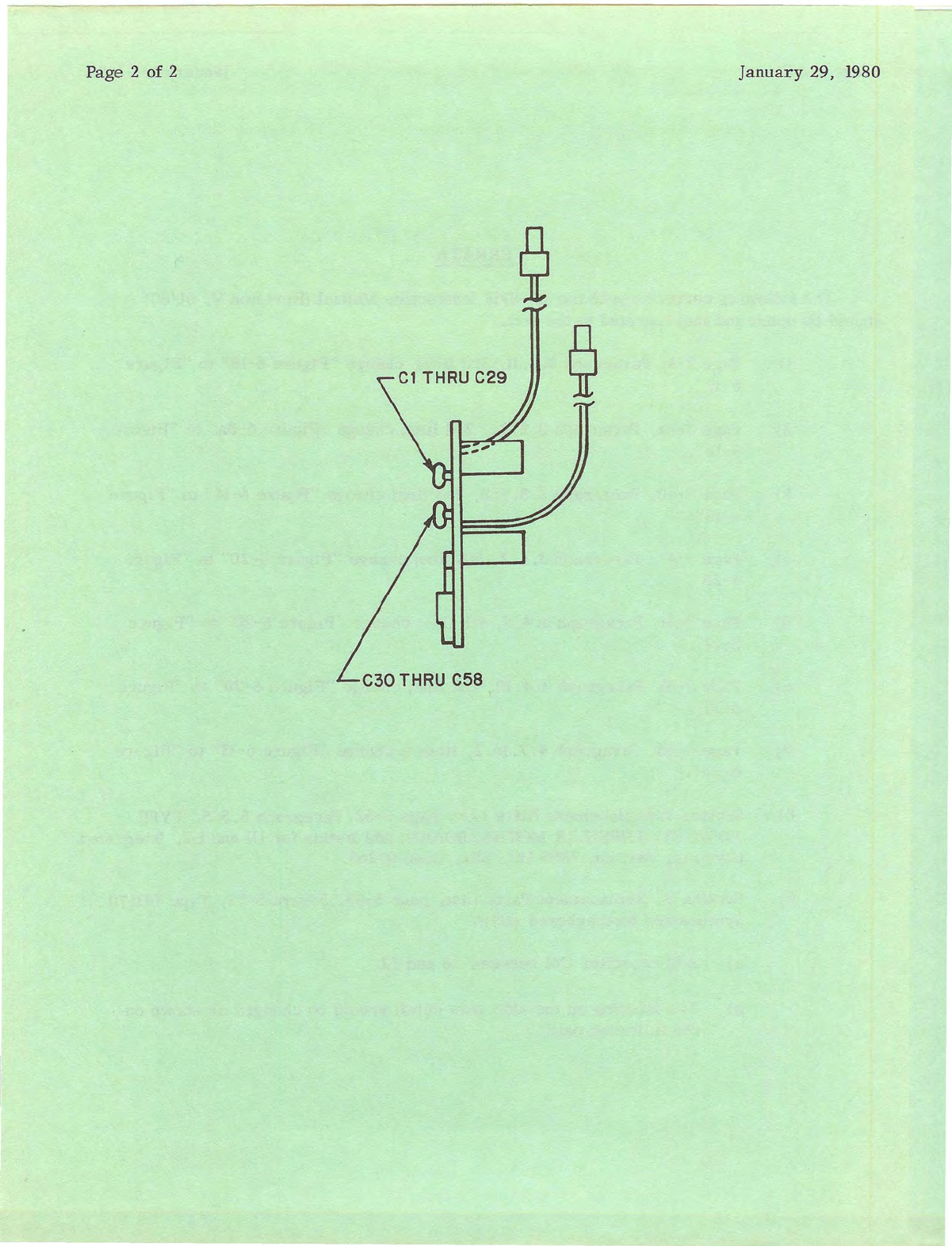
9)
Section
V,
Replacement
Parts
List,
page
5-53,
Figure
5-52,
Type
791570
Synthesizer
Motherboard
(A5);
a)
Add
capacitor
C61
between
L3
and
LI.
b)
The
labeling
on
the
side
view
detail
should
be
changed
as
shown
on
the
following
page.
Courtesy of http://BlackRadios.terryo.org
Page 2
of
2
Cl THRU C29
C30THRU
C58
January
29, 1980
Courtesy of http://BlackRadios.terryo.org
Table of contents
Other Watkins Johnson Receiver manuals


