Wavelength Electronics FL500 User manual

406-587-4910
www.teamWavelength.com
FL500
Single 500 mA or Dual 250 mA Channel Laser Diode Driver
DATASHEET AND OPERATING GUIDE
ORDERING INFORMATION
PART NO DESCRIPTION
FL500 500 mA Laser Diode Driver
FL591FL 500 mA Laser Diode Driver and Board
FLEXIBILITY YOU NEED
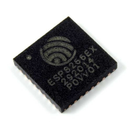
The FL500 Laser Diode Driver comes in a small SMT
package that is reow process compatible.
The FL500 is ideal for driving low power laser diodes. It
operates from 3 to 12 V, so it is compatible with Li+ battery
operation. This makes it practical for handheld devices.
It can be congured as two totally independent 250 mA
drivers or a single 500 mA driver. It is compatible with
Type A or Type B laser diodes.
FEATURES
• Small Package: 0.75” x 0.45” x 0.255”
• Low Cost
• Brownout Protection
• 12-Pin, SMT Package, Reow Compatible
• Slow Start Laser Diode Protection
• Drive Up to 500 mA Output Current
• Can be congured as two 250 mA drivers
• Voltage Controlled Setpoint
• TTL Compatible Shutdown Pin
• Adjustable Current Limit on Evaluation Board
• Adjustable Current Range Output
• 500 kHz sinewave Constant Current Bandwidth
(100 kHz square wave)
CONTENTS
QUICK CONNECT GUIDE 2
PIN DESCRIPTION 4
ELECTRICAL SPECIFICATIONS 5
SAFETY INFORMATION 7
OPERATING INSTRUCTIONS 8
ADDITIONAL TECHNICAL INFORMATION 10
TROUBLESHOOTING 11
MECHANICAL SPECIFICATIONS 12
CERTIFICATION AND WARRANTY 13
e
PAGE
Pb
RoHS
Compliant
© October 2020
EASY INTEGRATION
The FL500 allows for quick and easy operation in Constant
Current (CC) mode. For simple CC mode operation the
only components that are required are a power supply,
an analog control voltage, your laser and optional ltering
circuitry.
For additional features, including current limit and
photodiode feedback for Constant Power operation, use
with the FL591FL driver board.
LEADING EDGE APPLICATIONS
The FL500 is commonly used in hand-held, portable, and
space constrained applications. Small and light weight,
the FL500 is ideal for airborne applications, spectroscopy
systems, and the dual-channel output is perfect for
sighting-and-detection applications.
A
Laser Type
B
Laser Type

QUICK CONNECT GUIDE
FL500 Pin Layout page 2
FL500 Connection Diagrams page 2
FL500 Test Loads page 3
FL500 Block Diagram page 7
!
Toensure safe operaTion of The fL500 Driver,
iT is imperaTive ThaT you DeTermine ThaT The uniT wiLL be
operaTing wiThin The inTernaL heaT DissipaTion safe
operaTing area (soa).
Visit the Wavelength Electronics website for the most
accurate, up-to-date, and easy to use SOA calculator:
https://www.teamwavelength.com/support/design-tools/soa-ld-calculator/ Figure 1. FL500 Top View Pin Layout
Figure 2. Dual 250 mA drivers conguration
Figure 1 shows the top view Pin layout of the FL500 driver.
Figure 2 shows connection diagram for FL500 driver in dual
conguration.
VDD
GND
RESET
VSET1
GND
VSET2
LDC1
LDC1
PGND
PGND
LDC2
LDC2
1
2
3
4
5
6
12
11
10
9
8
7
D1
U1
FL500
ENABLE
VSET
0.1 µF 1 µF
R1
10Ω
VS
Figure 3. Single 500 mA driver conguration
Figure 3 shows connection diagram for FL500 driver in
single conguration.
© 2020 www.teamWavelength.com 2
FL500 LASER DIODE DRIVER

QUICK CONNECT GUIDE, CONTINUED
The FL500 is compatible with Type A and Type B lasers, but
will not drive Type C lasers: see Figure 4.
Type A Laser Diode Type B Laser Diode Type C Laser Diode
Common
Cathode
Laser Diode Anode &
Photodiode Cathode Common Isolated Photodiode
Short the
Laser Diode Anode
to Photodiode Cathode
Common
Anode
Laser Diode Cathode &
Photodiode Anode Common
Figure 4. Laser Type Diagrams
LASER DRIVER TEST LOADS
Figure 5 shows a recommended simulated laser load for
Type A and Type B lasers in Constant Current Mode. To
determine the actual drive current, measure the voltage
drop across the 1 Ω resistor. Do no insert an ammeter in
series with the output circuit; doing so may cause instability
in the control loop.
12
11
1 Ω
2 W
1N4001
1N4001 VDD
LDC
LDA
Figure 5. Laser Driver Test Load
© 2020 www.teamWavelength.com 3
FL500 LASER DIODE DRIVER

PIN DESCRIPTION
Table 1. Pin Descriptions
PIN
LABEL
PIN # NAME PIN DESCRIPTION
VDD 1 Control Electronics Power Power supply input for the FL500’s internal control electronics. Supply range
input for this pin is +3 to +12 Volts DC. It is compatible with Li+ batteries.
GND 2 Control Electronics Ground Return path for control electronics. Connect ground for VDD power supply
here. Do not use for high current ground return.
RESET 3Enable / RESET Control
TTL compatible. LO = laser diode current on
FLOAT or HI = laser diode current attenuated to ~10 µA
(~20 µA if drivers are paralleled to produce 500 mA)
VSET1 4 Setpoint for LDC1 control
2 kΩ input impedance. 0 to 2 V range. There is no internal clamping, so
higher voltage here will produce more current through the laser diode.
Not recommended above 2 V.
GND 5 Ground for setpoint inputs Low Current, Low Noise ground for use with VSET1 & VSET2.
VSET2 6 Setpoint for LDC2 control
2 kΩ input impedance. 0 to 2 V range. There is no internal clamping, so
higher voltage here will produce more current through the laser diode.
Not recommended above 2 V.
LDC2
LDC2
7
8
Laser Diode Cathode,
Driver 2
Tie to laser diode cathode for individual drive operation (250 mA max).
Tie to LDC1 for parallel operation up to 500 mA.
Tie to pin 8 (also LDC2) if laser diode current exceeds 125 mA. Actual pin
capacity is greater, but higher current produces offsets and higher noise.
PGND
PGND
9
10
Power Ground for VS
connection (VS powers
laser diode)
Use for ground connection of VS power supply.
Tie to pin 10 (also PGND) if laser diode current exceeds 125 mA.
LDC1
LDC1
11
12
Laser Diode Cathode,
Driver 1
Tie to laser diode cathode for individual drive operation (250 mA max).
Tie to LDC2 for parallel operation up to 500 mA.
Tie to pin 12 (also LDC1) if laser diode current exceeds 125 mA. Actual pin
capacity is greater, but higher current produces offsets and higher noise.
© 2020 www.teamWavelength.com 4
FL500 LASER DIODE DRIVER

ELECTRICAL SPECIFICATIONS
PARAMETER SYMBOL MIN TYP MAX UNIT
ABSOLUTE MAXIMUM RATINGS
Supply Voltage (Voltage on Pin 1) VDD +3 +12 * Volts DC
Output Current (See SOA Chart) IOUT 500 mA
Power Dissipation, TAMBIENT = +25ºC [1] PMAX 2 Watts
Operating Temperature, case TOPR - 40 +85 ºC
Storage Temperature TSTG - 55 +125 ºC
Weight FL500 0.08 oz
PARAMETER TEST CONDITIONS MIN TYP MAX UNIT
CONSTANT CURRENT CONTROL
Short Term Stability, 1 hour TAMBIENT = +25ºC 35 40 ppm
Long Term Stability, 24 hours TAMBIENT = +25ºC 50 75 ppm
CONSTANT POWER CONTROL
Short Term Stability, 1 hour [2] 0.019 %
Long Term Stability, 24 hours [2] 0.011 %
OUTPUT [3]
Current, peak, see SOA chart Per channel 245 250 252 mA
Current, peak, see SOA chart Two channels operated
in parallel 495 500 505 mA
Compliance Voltage, Laser Diode
Load
Full Temperature Range,
IOUT = 500 mA VDD - (0.5 x VSET)V
Rise Time IOUT = 500 mA 300 nsec
Fall Time IOUT = 500 mA 300 nsec
Bandwidth (Constant Current) Sine Wave 500 kHz
Bandwidth (Constant Current) Square Wave 100 kHz
Delayed Start 100 msec
Slow Start ramp rate 15 mA / msec
Depth of Modulation 100 kHz sine wave 99 %
Transfer Function - VSET to IOUT Two 250 mA drivers 0.125 A / V
Transfer Function - VSET to IOUT One 500 mA driver 0.25 A / V
POWER SUPPLY
Voltage, VDD 312 * V
Current, VDD supply, quiescent 2.2 2.7 4.6 mA
VS, Maximum to LD Anode 20 * V
*The FL591 Evaluation Board revision A or B limits the input voltage to 9 V. Revision C allows full range operation from +3 V to +12 V.
Note [1]. Maximum Power Dissipation is 1 Watt per channel. When congured as one driver, maximum power dissipation is 2 W.
Note [2]. Constant Power Control is available with the FL591FL diode driver and board as well as the FL500 with the LDTC0520/1020
combination boards.
Note [3]. Limit is xed at 500 mA (250 mA per channel). The Evaluation Board circuitry adds a variable limit circuit.
© 2020 www.teamWavelength.com 5
FL500 LASER DIODE DRIVER

PARAMETER TEST CONDITIONS MIN TYP MAX UNITS
INPUT
Offset Voltage, initial, IMON Pin 2, TAMBIENT = +25ºC,
VCM = 0 V 2 mV
Bias Current (based on input Res of op amp) Pin 2, TAMBIENT = +25ºC,
VCM = 0 V 10 15 nA
Common Mode Range Pin 2, Full Temp. Range 0 VDD V
Common Mode Rejection, Setpoint Full Temperature Range -16 64 dB
Power Supply Rejection Full Temperature Range 60 dB
THERMAL
Heatspreader Temperature Rise TAMBIENT = +25ºC 43 ºC / W
Pin Solderability Solder temp @260ºC 10 Sec
NOISE
Noise & Ripple (RMS) IOUT = 100 mA, 100 kHz
bandwidth 3µA
Leakage Current
(when using the FL591 circuitry)
VSET = 0 V
VSET = 1 V
VSET = 2 V
50
100
150
µA
µA
µA
ELECTRICAL SPECIFICATIONS CONTINUED
© 2020 www.teamWavelength.com 6
FL500 LASER DIODE DRIVER

RESET
(Active Low,
TTL compatible
VDD GND
LDC1
LDC1
LDC2
LDC2
PWR GND
(for LD VS)
PWR GND
(for LD VS)
VSET 1
VSET 2
(Impedance:
2kΩ per driver,
1kΩ when
paralleled)
GND (forVSET)
VS
LD
VDD
SAFETY INFORMATION
SAFE OPERATING AREA — DO NOT EXCEED
INTERNAL POWER DISSIPATION LIMITS
Before attempting to operate the FL500 driver, it is imperative
that you rst determine that the unit will operate within the
Safe Operating Area (SOA). Operating outside of the SOA
may damage the laser and the FL500. Operating outside of
the SOA will void the warranty.
To determine if the FL500 driver will be operating in the
safe range in your application, consult the instructions for
calculating the Safe Operating Area online:
www.teamwavelength.com/support/design-tools/soa-ld-calculator/
SOA charts are included in this datasheet for quick reference
(page 11), but we recommend you use the online tools
instead.
Toensure safe operaTion of The fL500 Driver, iT
is imperaTive ThaT you DeTermine if The uniT is going
To be operaTing wiThin The inTernaL heaT DissipaTion
safe operaTing area (soa).
If you have any questions about the Safe Operating Area
calculator, call the factory for free and prompt technical
assistance.
PREVENT DAMAGE FROM ELECTROSTATIC
DISCHARGE
Before proceeding, it is critical that you take precautions to
prevent electrostatic discharge (ESD) damage to the driver
and your laser. ESD damage can result from improper
handling of sensitive electronics, and is easily preventable
with simple precautions.
For more information regarding ESD, see Application Note
AN-LDTC06: Basics: Electrostatic Discharge (ESD).
We recommend that you always observe ESD precautions
when handing the FL500 driver and your laser diode.
!
THEORY OF OPERATION
The FL500 driver is a controlled current source: it delivers
the current commanded by the setpoint. The current source
continually monitors the actual output current, compares it to
the setpoint, and adjusts the current if there is a difference
between the two signals.
It may be useful to remember that you do not directly set the
driver current setpoint; instead, you adjust a voltage signal
that represents the output current. The voltage and output
current are related by a transfer function that varies by driver
capacity. The setpoint voltage is adjusted with an external
input.
As current is driven through the load, there is a voltage drop
across the load because of the impedance. As the current
increases, the voltage drop may increase to the point that it
reaches the Compliance Voltage limit of the current source.
Once that occurs, the current source is no longer able to
increase the current driven to the load even if you increase
the setpoint.
Figure 6 shows the block diagram of the FL500.
The FL500 driver includes features that help protect your
laser and make the driver more versatile in a wide array of
applications: handheld devices, airborne applications, and
spectroscopy systems.
Figure 6. FL500 Block Diagram
© 2020 www.teamWavelength.com 7
FL500 LASER DIODE DRIVER

OPERATING INSTRUCTIONS
The FL500 requires minimal external electronics. If you are
using the driver on the benchtop or for prototyping your laser
control system, we recommend purchasing the FL591FL
Driver Board.
We recommend using a test load until you are familiar with
operation of the driver. Refer to page 3 for test load
schematics.
NECESSARY EQUIPMENT
The following equipment is the minimum necessary to
congure the FL500 for basic operation:
• FL500 Driver
• Digital Voltmeter, 4-½ digit resolution recommended
• Test load for conguring the driver [optional]
• Laser Diode
• Connecting wires
• Power Supply
STEP 1 - CHOOSE ONE OR TWO POWER
SUPPLIES, VOLTAGES SOURCES
Congure the power supply to provide +3 to +12 VDC.
Connect the positive terminal of the power supply (VS) to
Pin 1 and the negative terminal to Pins 9 and/or 10 (PGND)
or Power Ground depending on the FL500 operation
explained in the following steps below. Only ground VSto
Pin 2 if it is also grounded to Pins 9 or 10 (see page 9).
VS powers the laser diode current source (or test load),
and VDD powers the control electronics. Power the laser
diode from VDD by connecting VDD where VSis shown.
For lower noise operation, separate VDD from VS. VScan
be up to 20 V. At this level, however, too much power can
be dissipated in the FL500 causing permanent damage.
Calculate the power dissipated in the FL500 using the Safe
Operating Area (SOA) Calculator online prior to using a
VSmore than 2 V greater than the voltage dropped over
the laser diode. A maximum power dissipation of 1 W
per source (2 W for paralleled operation) must not be
exceeded.
The minimum VS is determined by the voltage drop across
the laser diode and half the setpoint voltage. VSMIN = VLD +
VSET/2 + 25 mV (across FET). Ground this power supply
at Pins 9 & 10 (PGND). Using Pin 2 could damage the
FL500.
Example VSMIN:
VLD = 1.2 V
VSET = 1.5 V
VSMIN = 1.2 V + (1.5 / 2) + 0.025 = 1.975
STEP 2 - CREATE A SETPOINT
Connect a voltage source to Pins 4 (VSET1) and/or Pins 6
(VSET2) and Pin 5 (GND) to create a setpoint for the current
output. Check the specic conguration step below for more
detailed instructions.
Pick the one of the following three wire congurations
(step 3) that best ts your operation of the FL500.
STEP 3 - CONFIGURE THE WIRING
OPTION 1: OPERATE AS TWO INDEPENDENT
DRIVERS
Connect the positive terminal of a power supply to Pin 4
(VSET1) and the positive terminal of another power supply
to Pin 6 (VSET2). Connect both negative terminals to
Pin 5 (GND). The power supplies do not need to be tied
together. The transfer function for individual VSETs (1 & 2)
is 0.125 A / V. The FL500 contains circuitry for two 250 mA
drivers.
Connect one test load (laser diode) to Pins 11 & 12 (LDC1)
and Pin 1 (VDD). Place the other test load on Pins 7 & 8
(LDC2) and Pin 1 (VDD). Make sure VS is grounded at Pins 9
& 10 (PGND). Pin 2 (GND) will also be tied to this ground.
The RESET minimum current is 10 µA, and the leakage
current is less than 1 mA. The FL500 has a known leakage
current when disabled equal to the following magnitude:
IOUT(LEAK) =VIN
20 kΩ
This is well below 1 mA, and the usual leakage expected is
100 µA.
See Figure 7 for typical operating schematic.
Figure 7. Single Supply Voltage Operating Two Independent
Drivers
Leave Pins 6, 7, 8, and either 9 or 10 oating (or not
connected to a power supply or ground) to limit the output
current of the FL500 to 250 mA by using just one channel.
© 2020 www.teamWavelength.com 8
FL500 LASER DIODE DRIVER
OPTION 2: OPERATE IN PARALLEL AS ONE
DRIVER
Use only one power supply to power Pins 4 & 6 (VSET1 &
VSET2) with ground at Pin 5 (GND). Wire the test load (laser
diode) to Pins 7 & 8 (LDC2), Pins 11 & 12 (LDC1), and to
Pin 1 (VDD). The FL500 contains circuitry for two 250 mA
drivers. They can be run in parallel to deliver 500 mA to one
laser diode (see OPTION 1: Operate as two independent
drivers for single channel output current of 250 mA setup).
Tie LDC1 & LDC2 together. VSET1 and VSET2 can be
tied together or one can be used to set a DC bias while the
other is used for an additive modulation signal. Only one VS
can be used. The transfer function for tied VSET(1 & 2) is
0.25 A / V.
The RESET minimum current is 20 µA, and the leakage
current is 2 mA. Note that if VSETs are tied together, input
impedance becomes two 2 kΩ in parallel or 1 kΩ. The FL500
has a known leakage current when disabled equal to the
following magnitude:
IOUT(LEAK) =VIN
20 kΩ
This is well below 1 mA, and usual leakage expected is
100 µA.
See Figure 8 for typical operating schematic.
Figure 8. Parallel Operation as One Driver
OPTION 3: OPERATE MULTIPLE FL500S IN
PARALLEL
Tie LDC1 & LDC2 (Pins 7 & 8, 11 & 12) on each FL500
together and wire the test load to these pins and Pin 1
(VDD). Tie PGND (Pins 9 & 10) together and use to ground
VS. Ground Pin 2 as well. Tie each Pin 3 (RESET) together
and ground to enable current to the load. Tie each VSETs
(Pins 4 & 6) together and wire the other power supply to
these pins with ground at Pins 5 (both grounded).
Multiple FL500s can be used in parallel for 1 A, 1.5 A, etc.
operation: Note input impedance on VSET drops. For two
FL500s congured for 500 mA each and used in parallel, the
input impedance drops to 500 Ω.
See Figure 9 for typical operating schematic.
Figure 9. Multiple Units in Parallel Operation
STEP 4 - RESET / ENABLE FUNCTION [PIN3]
Ground Pin 3 to enable output current to the laser diode.
This control pin is common to both sources. When active,
this pin attenuates the output current amplitude to near zero
(~10 µA when congured for 250 mA max and ~20 µA if
drivers are paralleled to produce 500 mA). Current still ows
through the laser diode. The pin is active LO.
LO = LD current owing to setpoint.
FLOAT or HI = LD current attenuated.
The input is TTL compatible.
BROWN OUT PROTECTION
If VDD drops below 2.7 V, the RESET circuit is triggered
immediately (on the order of 100 µsec), reducing current
through the laser diode to attenuated levels (~10 µA).
© 2020 www.teamWavelength.com 9
FL500 LASER DIODE DRIVER
DELAYED / SLOW START
Once power is applied, current at the attenuated level will ow
(~10 µA when congured for 250 mA max). After 100 msec,
current will rise to the level dictated by the setpoint voltage
at the rate of about 15 mA / msec. This delay ensures that
all control electronics are functioning before signicant
current ows to the laser diode. The delay time is set with
internal components. [It can be increased - please request a
modication through Sales.] Refer to Figure 10 for a typical
sequence.
CURRENT LIMIT
To set current limits, use the circuit below from the FL591
schematic. To set two current limits (one for each individual
driver), use the same circuit to also connect to VSET2.
CONSTANT POWER MODE
To operate in Constant Power mode with photodiode
feedback, use the circuit below from the FL591 schematic.
PDA1
PDR1
R10
1.0K
1.0K
R7
1.0K
R2 R3
1.0K 1.0K
1.0K
U1A
VS-U1
VEE-U1
AD8032
PMON1
PSET1
R4
R6
1.0K
1.0K
100K
0.012µF
VCC-U3
VEE-U3
PDFB1
AD8032
R9
C4
0.022µF
2
3
48
1
C1
R1
2
3
48
1
Figure 10. Typical Delayed / Slow Start Response
D8
LM4040-2.5
5
43
Q4A
2
1 6
Q4B
MMDT3946
R84
249
2
31
W
CW
CCW
R82
2.0K
C46
10uF
C47
10uF
R81
182
VCC
2
3
1
84
U4A
AD8032
2
3
1
84
U6A
AD8032
VCC-U4
VCC-U6
VEE-U6
R78
1.05K
VCC
R61
10.0
VCC
1
GND
2
RST
3
VSET1
4
GND
5
VSET2
6LDC2
LDC2
PGND
PGND
LDC1
LDC1
U5
FL500
C26
10uF
C48
10uF
D7
1N4148
VSET1
R77
1.0K
R76
1.0K
R85
1.0K
R75
1.0K
R83
1.0K
R86
2.0K
TP2
LIM1
© 2020 www.teamWavelength.com 10
FL500 LASER DIODE DRIVER

ADDITIONAL TECHNICAL
INFORMATION
SAFE OPERATING AREA
The Safe Operating Area of the FL500 laser diode driver is
determined by the amount of power that can be dissipated
within the output stage of the driver. If that power limit is
exceeded permanent damage can result.
DonoT exceeD The safe operaTing area
(soa). exceeDing The soa voiDs The
warranTy.
Refer to the Wavelength Electronics website for the most
up-to-date SOA calculator for our products. The online tool
is fast and easy to use, and also takes into consideration
operating temperature.
www.teamwavelength.com/support/design-tools/soa-ld-calculator/
SOA charts are included in this datasheet for quick reference,
however we recommend you use the online tools instead.
An example SOA calculation for the FL500 for 1 W, 250 mA
for independent channels operation is shown in Figure
11 where:
VS= 5 Volts (Point C) VLOAD = 2.5 Volts
ILOAD = 100 mA (Point B) VDROP = 5 - 2.5 = 2.5 Volts (Point A)
Unsafe Operating Area
Voltage Drop Across FL500 (V
S
- V
LOAD
) (
V
)
Maximum Current LDC1 or LDC2 (A)
FL500 Safe Operating Area
Independent Channels 1 W, 250 mA max
B BB
A C
25ºC Ambient
35ºC Case
Figure 11. FL500 Independent Channels SOA
!
Follow these steps to determine if the driver will be operating
within the SOA.
• Refer to the laser datasheet to nd the maximum voltage
(VLOAD) and current (ILOAD) specications
• Calculate the voltage drop across the driver: VDROP =
VS- VLOAD (VS is the power supply voltage)
• Mark VDROP on the X-axis, and extend a line upward
• Mark ILOAD on the Y-axis, and extend a line (Line BB) to
the right until it intersects the VDROP line
• On the X-axis, mark the value of VS
• Extend a diagonal line from V+ to the intersection of the
VDROP and ILOAD lines; this is the Load Line
• If the Load Line crosses the Safe Operating Area line at
any point, the conguration is not safe
If the SOA Calculator indicates the FL500 will be outside of
the Safe Operating Area, the system must be changed so that
less power is dissipated within the driver. See Wavelength
Electronics Application Note AN-LDTC01: The Principle of
the Safe Operating Area for information on shifting the Load
Line.
An example SOA calculation for the FL500 for 2 W, 500 mA
for parallel channels operation is shown in Figure 12 where:
VS = 3 Volts (Point C) VLOAD = 2 Volts
ILOAD = 400 mA (Point B) VDROP = 3 - 2 = 1 Volts (Point A)
Figure 12. FL500 Parallel Channels SOA
B BB
A C
Unsafe Operating Area
FL500 Safe Operating Area
Parallel Channels 2 W, 500 mA max
Voltage Drop Across FL500 (VS- VLOAD) (V)
25ºC Ambient
35ºC Case
Maximum Current LDC1 or LDC2 (A)
© 2020 www.teamWavelength.com 11
FL500 LASER DIODE DRIVER
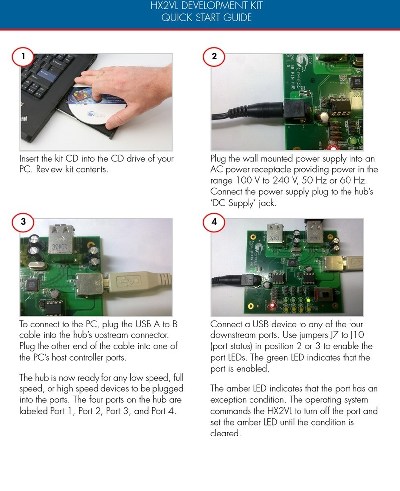
TROUBLESHOOTING
PROBLEM POTENTIAL CAUSES SOLUTIONS
Driver will not switch on Improperly congured power supply
Carefully check the wiring diagram according to page 8 and
page 9.
If operating the FL500 with the Evaluation Board, see the
FL591FL Datasheet for details regarding power supply.
Output will not enable ENABLE Pin not held low Refer to the RESET/ENABLE control (Pin 3) in Table 1 on
page 4.
Laser output power too low in
Constant Current mode
Laser voltage setpoint too low
Increase the setpoint by increasing the voltage at Pin 4 & 6
(VSET1 & VSET2). VSET1 & VSET2 may be tied together if
operating in parallel.
Laser current limit too low The current limit is xed at 500 mA (250 mA per channel).
The Evaluation Board circuitry adds a variable limit current.
Laser driver is compliance limited
Check the laser diode specications to determine the forward
voltage (VF). Make sure that the FL500 is not compliance
limited.
Refer to the Electrical Specications table on page 5. If the
driver is compliance limited, VDD may need to be increased.
Verify that the FL500 will be operating within the Safe
Operating Area if VDD is increased.
Driver will not operate in
Constant Power mode
Not available with the standalone
driver
Constant Power Control is available when the FL500 is
used with the FL591 (Evaluation Board) as well as the
LDTC0520/1020 combination modules.
Transfer functions are
inaccurate
Operating as two 250 mA drivers
instead of one 500 mA driver or
reverse
The Transfer Function for operation as two 250 mA drivers is
0.125 A / V.
The Transfer Function for operation as one 500 mA driver is
0.25 A / V.
This is seen in the Electrical Specications table on page 5.
© 2020 www.teamWavelength.com 12
FL500 LASER DIODE DRIVER

MECHANICAL SPECIFICATIONS
FL500 IS REFLOW PROCESS COMPATIBLE.
All dimensions are ±5%
0.75”
[19.1 mm]
0.047”
[1.19 mm]
0.125”
[3.2 mm]
0.45”
[11.4 mm]
0.48”
[12.2 mm]
0.040”
[1.02 mm]
0.55”
[13.8 mm]
0.26”
[6.5 mm] 0.035”
0.89 mm
0.45”
[11.4 mm]
0.100”
[2.5 mm]
0.085”
[2.2 mm]
0.100”
[2.5 mm]
0.018”
[0.46 mm]
0.75”
[19.1 mm]
PCB FOOTPRINT
© 2020 www.teamWavelength.com 13
FL500 LASER DIODE DRIVER

CERTIFICATION AND WARRANTY
CERTIFICATION
Wavelength Electronics, Inc. (Wavelength) certies that this
product met its published specications at the time of shipment.
Wavelength further certies that its calibration measurements are
traceable to the United States National Institute of Standards and
Technology, to the extent allowed by that organization’s calibration
facilities, and to the calibration facilities of other International
Standards Organization members.
WARRANTY
This Wavelength product is warranted against defects in materials
and workmanship for a period of one (1) year from date of shipment.
During the warranty period, Wavelength will, at its option, either
repair or replace products which prove to be defective.
WARRANTY SERVICE
For warranty service or repair, this product must be returned to the
factory. An RMA is required for products returned to Wavelength
for warranty service. The Buyer shall prepay shipping charges to
Wavelength and Wavelength shall pay shipping charges to return
the product to the Buyer upon determination of defective materials
or workmanship. However, the Buyer shall pay all shipping charges,
duties, and taxes for products returned to Wavelength from another
country.
LIMITATIONS OF WARRANTY
The warranty shall not apply to defects resulting from improper use or
misuse of the product or operation outside published specications.
No other warranty is expressed or implied. Wavelength specically
disclaims the implied warranties of merchantability and tness for
a particular purpose.
EXCLUSIVE REMEDIES
The remedies provided herein are the Buyer’s sole and exclusive
remedies. Wavelength shall not be liable for any direct, indirect,
special, incidental, or consequential damages, whether based on
contract, tort, or any other legal theory.
REVERSE ENGINEERING PROHIBITED
Buyer, End-User, or Third-Party Reseller are expressly prohibited
from reverse engineering, decompiling, or disassembling this
product.
NOTICE
The information contained in this document is subject to change
without notice. Wavelength will not be liable for errors contained
herein or for incidental or consequential damages in connection
with the furnishing, performance, or use of this material. No part of
this document may be translated to another language without the
prior written consent of Wavelength.
SAFETY
There are no user-serviceable parts inside this product. Return the
product to Wavelength Electronics for service and repair to ensure
that safety features are maintained.
LIFE SUPPORT POLICY
This important safety information applies to all Wavelength
electrical and electronic products and accessories:
As a general policy, Wavelength Electronics, Inc. does not
recommend the use of any of its products in life support applications
where the failure or malfunction of the Wavelength product can
be reasonably expected to cause failure of the life support device
or to signicantly affect its safety or effectiveness. Wavelength
will not knowingly sell its products for use in such applications
unless it receives written assurances satisfactory to Wavelength
that the risks of injury or damage have been minimized, the
customer assumes all such risks, and there is no product liability
for Wavelength. Examples of devices considered to be life support
devices are neonatal oxygen analyzers, nerve stimulators (for
any use), auto-transfusion devices, blood pumps, debrillators,
arrhythmia detectors and alarms, pacemakers, hemodialysis
systems, peritoneal dialysis systems, ventilators of all types, and
infusion pumps as well as other devices designated as “critical”
by the FDA. The above are representative examples only and are
not intended to be conclusive or exclusive of any other life support
device.
REVISION HISTORY
DOCUMENT NUMBER: FL500-00400
REV. DATE CHANGE
FFeb. 2009 Updated to include FL500
Reow Oven compatibility
G Sept. 2009 Updated to reect RoHS Status
HJune 2013 Updated Noise & Ripple
specications
I Mar. 2014 Claried reow compatibility
J Dec. 2014 Updated to fully reow
compatible
K Nov. 2015 Updated leakage current
specication
L Oct. 2020 Updated to new format, added
current limit and PD feedback
WAVELE
n
GTH
ELECTRONICS
51 Evergreen Drive
Bozeman, Montana 59715
406-587-4910 (tel)
406-587-4911 (fax)
Sales & Tech Support
© 2020 www.teamWavelength.com 14
FL500 LASER DIODE DRIVER
This manual suits for next models
1
Table of contents