WAN_0264 Customer Information
w September 2011, Rev 1.0
Customer Information 10
USER KEY
Certain register bits are protected behind a User Key which locks down the functionality and only
enables the protected bits to be written to if the User Key (Unlock) has been previously written.
The user key is 9716h
Locked bits are identified with a small key symbol as shown above.
Note:
It is recommended to relock the protected register immediately after writing to them. This helps protect
the system against accidental overwriting of register values. To lock the protected registers, a value of
0000h should be written to the Security register.
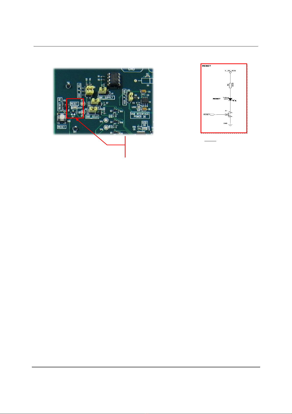
STATUS LED1 AND LED2
STATUS LED1 AND LED2 SET-UP
The WM832x provides two System Status LED drivers. These are digital outputs intended for driving
LEDs directly. The LED outputs can be assigned to indicate Power State status and other control
features. They can also be controlled via register control to provide a custom indication.
Examples:
R404Ch = Status LED1 (below LED1_SRC=10= Reserved status)
LED1 also indicates completion of OTP Auto Program.
R404Dh= Status LED2 (below LED2_SRC=01= Power State status)
POWER STATE STATUS
DESCRIPTION DRIVE MODE LED ‘ON’ TIME ON:OFF DUTY
CYCLE
Power Sequence Failure Pulsed sequence (4 pulses) 1s 1:1
PVDD low Continuous pulsed 250ms 1:3
ON state Constant N/A N/A
SLEEP state Continuous pulsed 250ms 1:7
LED1&LED2 LED1&LED2