WM8738-EV1M
WOLFSON MICROELECTONICS LTD Rev 2.1 August 2002
2
POWER SUPPLIES
Using appropriate power leads with 4mm connectors, +5V should be applied to the +5V panel socket
J1.
+3.0V to +3.6V should be applied to the DVDD panel socket J3 and +3.0V to +5.5V should be
applied to the AVDD panel socket J5.
+12V should be applied to the +12V panel socket J7 and -12V should be applied to the -12V panel
socket J10.
DGND should be connected to the DGND panel socket J2 and AGND to the AGND panel socket J6.
The DGND and AGND connections may be connected to a common GND on the supply with no
reduction in performance.
Note: Refer to WM8738 datasheet for limitations on individual supply voltages.
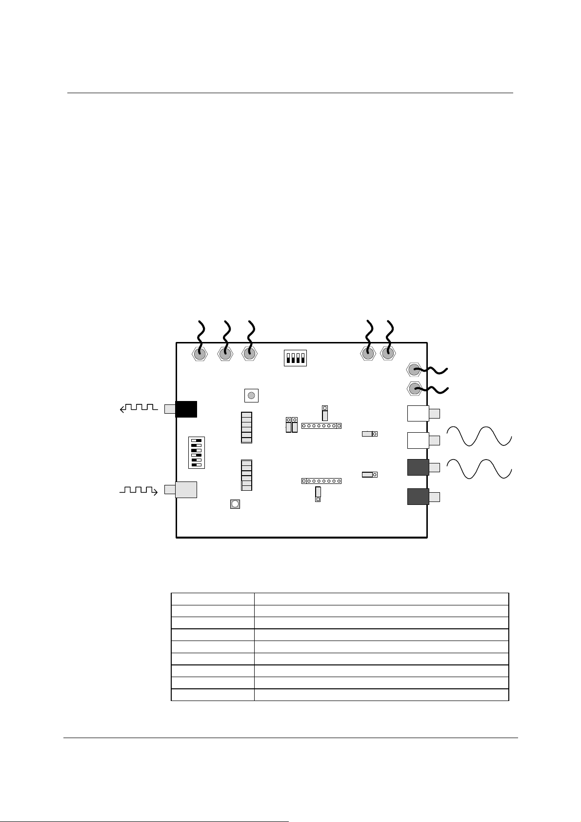
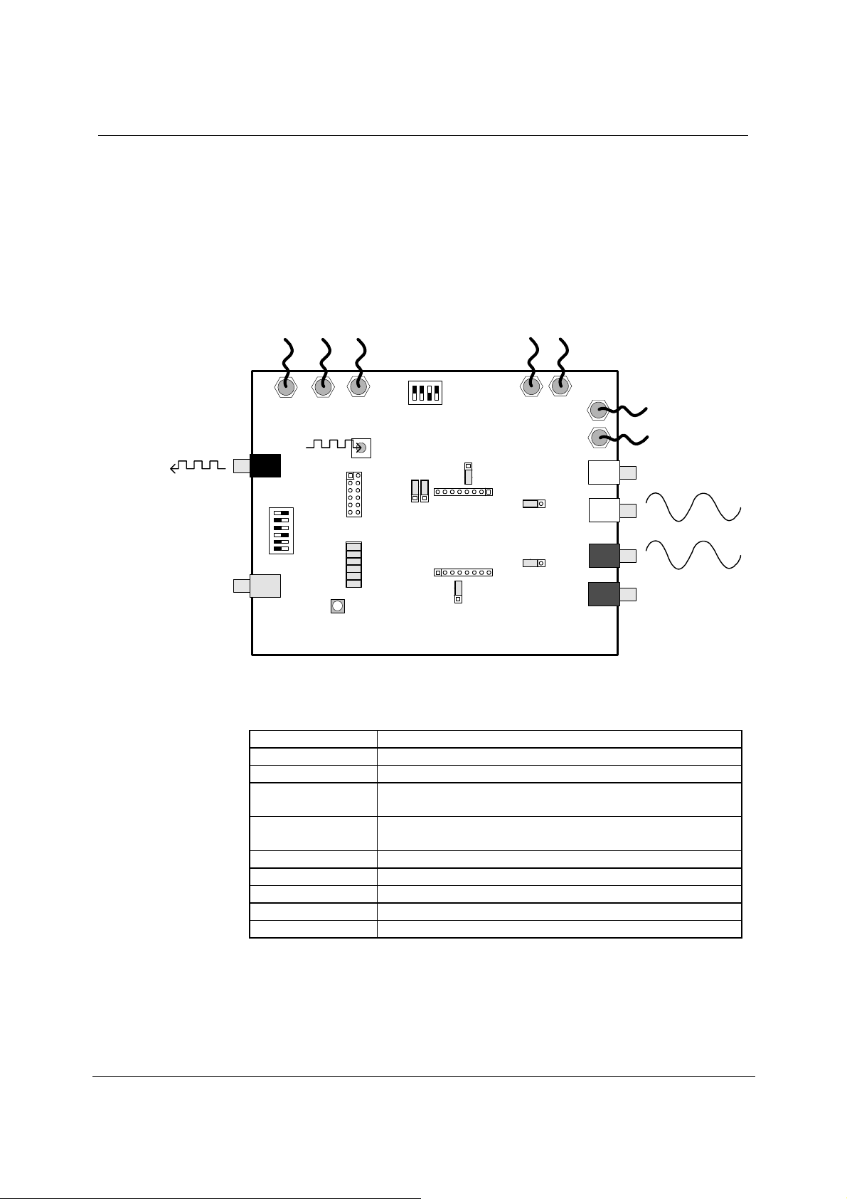
BOARD FUNCTIONALITY
There are three options for inputting the required digital clocks to the WM8738 evaluation board.
There is a coaxial input (J14) via a standard phono connector or a direct digital input is available via
one side of a 2x6 pin header (H1). A further option is to input a MCLK via connector J9 and use the
CPLD (U1) to generate BCLK and LRCLK.
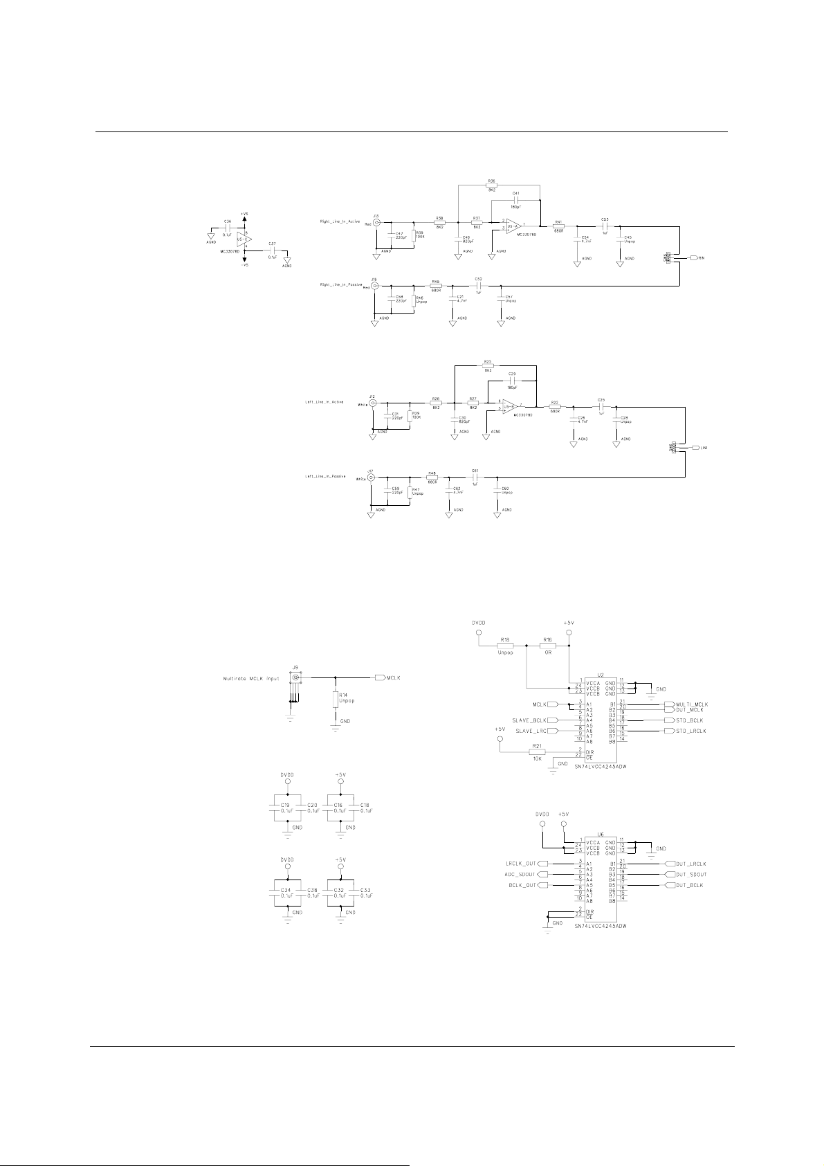
The analogue input signals are applied to the evaluation board via phono connectors through either
passive or active anti-alias filters. For passive filtering J17 (LIN) and J16 (RIN) can be used and for
active filtering J12 (LIN) and J13 (RIN).
There are two options for outputting digital data from the WM8738 evaluation board. There is a
coaxial output (J8) via a standard phono connector or the digital signals output from the WM8738
may be accessed via one side of a 2x6 pin header (H2).
All WM8738 device pins are accessible for easy measurement via the 8 pin headers (J11 & J15)
running up each side of the device.
BOARD INPUT
Analogue input to the WM8738 is selectable via switches SW5 and SW6. This allows the analogue
input to either pass through a passive anti-aliasing filter, using J17 (LIN) and JI6 (RIN), or an active
anti-aliasing filter, using J12 (LIN) and J13 (RIN).
Digital clock signals must be supplied to the WM8738. A digital (AES/EBU, UEC958, S/PDIF, EIAJ
CP340/1201) signal input may be applied to the coaxial input (J14), allowing the CS8427 (U3) to
generate the necessary clocks. A direct digital input is also available via one side of a 2x6 pin
header (H1). There is also the facility to generate multi-rate clocks from U1 using SW7 as the rate
selection and either the MCLK from the CS8427 (U3) or an independent MCLK input to SMB
connector J9.
The digital inputs of the WM8738 are +5V tolerant (independent of supplies), however, a level shift IC
(U2) has been included in the audio interface signal path to buffer the input signals when applied via
header (H1) and minimise any performance degradation this may cause..
Note: The level shift IC's (U2 and U6) are set to shift from +5V to DVDD when shipped from Wolfson.
BOARD OUTPUT
The output interface from the board is via a coaxial (J8) digital (AES/EBU, UEC958, S/PDIF, EIAJ
CP340/1201) signal output. A direct signal output is available via one side of a 2x6 pin header (H2).
Data is output in one of the WM8738 supported formats - see datasheet.
A level shift IC (U6) has been included in the audio output interface path to provide signal buffering
when output signals are taken from 2x6 pin header H2 will meet external receiver requirements.