Wolfson WM8510-EV1M Instruction Manual

WM8510-EV1M
Evaluation Board User Handbook
Rev 1.1

WM8510-EV1M
w Rev 1.1 April 2006
2
TABLE OF CONTENTS
TABLE OF CONTENTS.............................................................................................................2
INTRODUCTION ........................................................................................................................4
GETTING STARTED..................................................................................................................4
EVALUATION BOARD CHECKLIST .................................................................................................4
CUSTOMER REQUIREMENTS .......................................................................................................4
PCB MAIN CONNECTIONS ......................................................................................................5
POWER SUPPLIES ......................................................................................................................5
DIGITAL INPUT ...........................................................................................................................5
DIGITAL OUTPUT ........................................................................................................................6
ANALOGUE INPUT ......................................................................................................................6
ANALOGUE OUTPUT ...................................................................................................................7
USB CONNECTIONS ....................................................................................................................7
INTERFACES.............................................................................................................................8
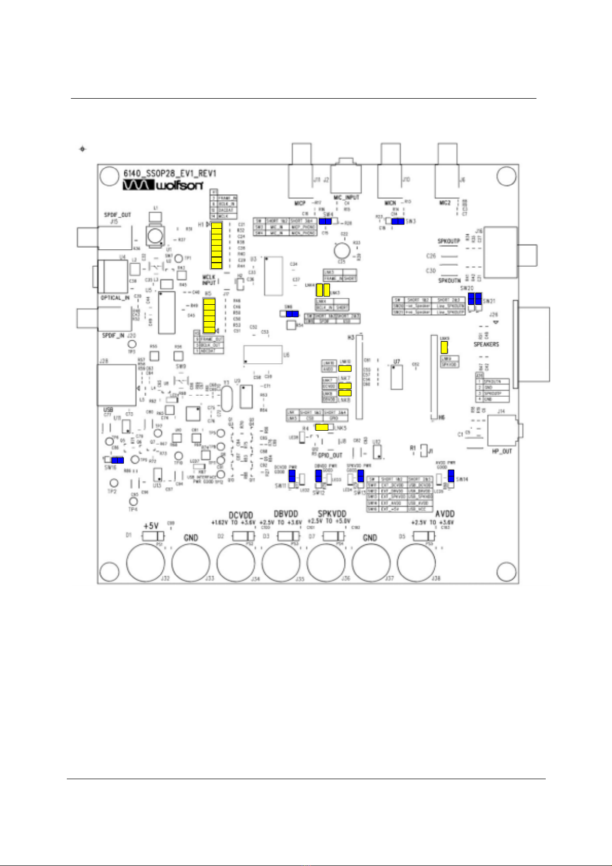
HEADERS ..................................................................................................................................9
LINKS AND JUMPERS ..................................................................................................................9
SWITCHES...............................................................................................................................10
SOFTWARE CONTROL ..........................................................................................................11
SELECTION OF CONTROL MODE ................................................................................................11
3-WIRE SERIAL CONTROL MODE ...............................................................................................11
2-WIRE SERIAL CONTROL MODE ...............................................................................................11
REGISTER MAP ......................................................................................................................13
WM8510 BLOCK DIAGRAM ...................................................................................................14
WM8510-EV1S CONTROL SOFTWARE DESCRIPTION.......................................................15
SOFTWARE DOWNLOAD ...........................................................................................................15
SOFTWARE INSTALLATION ........................................................................................................15
REGISTER WRITE CONTROL PANELS..........................................................................................16
SETUP TEXT FILES ...................................................................................................................19
DEFAULT SETUP - SLAVE MODE .........................................................................................20
ADDITIONAL HARDWARE CONFIGURATIONS....................................................................22
MASTER MODE SETUP ..............................................................................................................22
EXTERNAL POWER SUPPLIES SETUP .........................................................................................24
HPDETECT,HEADPHONE AND BTL SPEAKER SETUP ....................................................................26
SCHEMATIC LAYOUT.............................................................................................................28
PCB LAYOUT ..........................................................................................................................34
WM8510-EV1B BILL OF MATERIAL ......................................................................................37
APPENDICES...........................................................................................................................40
USB INTERFACE TROUBLESHOOTING...............................................................................40
MESSAGE BOX EXPLANATIONS -COMMUNICATIONS ISSUES ........................................................40
USB COMMUNICATIONS ISSUES.................................................................................................41
MESSAGE BOX EXPLANATIONS -FILE LOAD/SAVE FUNCTIONS .....................................................44

WM8510-EV1M
w Rev 1.1 April 2006
3
EXTERNAL DSP CONNECTION TO THE WM8510-EV1B ....................................................46
AUDIO INTERFACE CONNECTIONS .............................................................................................46
SOFTWARE INTERFACE ............................................................................................................48
EVALUATION SUPPORT ........................................................................................................50
IMPORTANT NOTICE..............................................................................................................51
ADDRESS:...............................................................................................................................51
REVISION HISTORY ...............................................................................................................52

WM8510-EV1M
w Rev 1.1 April 2006
4
INTRODUCTION
The WM8510 is mono codec with pseudo-differential microphone and additional auxiliary input. The
device is equipped with dedicated mono headphone and speaker output drivers.
This evaluation platform and documentation should be used in conjunction with the latest version of
the WM8510 datasheet. The datasheet gives device functionality information as well as timing and
data format requirements.
This evaluation platform has been designed to allow the user ease of use and give optimum
performance in device measurement.
GETTING STARTED
EVALUATION BOARD CHECKLIST
The following items are available from Wolfson:
•WM8510-EV1B Evaluation Board - 6140_SSOP28_EV1_REV1
•WM8510-EV1S Control Software (download from http://www.wolfsonmicro.com)
•WM8510-EV1M User Handbook (download from http://www.wolfsonmicro.com)
CUSTOMER REQUIREMENTS
PC requirements are:
•PC with USB connection
•Operating systems supported Win XP/2000
Minimum signal path requirements are:
•An analogue input source
•S/PDIF signal source
•S/PDIF receiving unit

WM8510-EV1M
w Rev 1.1 April 2006
5
PCB MAIN CONNECTIONS
POWER SUPPLIES
Power is supplied to the WM8510 USB interface via the USB connector. If preferred, it is also
possible to supply +5V power to the audio interface level shift buffers from external supplies to 4mm
connectors.
Using appropriate USB cable a +5V supply can be connected as described in Table 1.
REF-DES SOCKET NAME SUPPLY
J28 USB +5V
Table 1 USB Power Supply Connection
Using appropriate power leads with 4mm connectors, external supplies can be connected as
described in Table 2.
REF-DES SOCKET NAME SUPPLY
J32 +5V +5V
J33 GND 0V
J34 DCVDD +1.71V to +3.6V
J35 DBVDD +1.71V to +3.6V
J36 SPKVDD +2.5V to +5.0V
J37 GND 0V
J38 AVDD +2.5V to +3.6V
Table 2 External Power Supply Connections
Note: Refer to WM8510 datasheet for current limitations on individual supply voltages.
Important: Exceeding the recommended maximum voltage can damage EVB components.
Under voltage may cause improper operation of some or all of the EVB components.
DIGITAL INPUT
There are two methods to input the required digital signal clocks to the WM8510 audio interface. An
AES/EBU, UEC958, S/PDIF, EIAJ CP340/1201 signal from coaxial input via a standard phono
connector (J20) or direct digital input is available via one side of a 2x8 pin header (H1).
A level shift IC (U3) has been included in the digital input interface path to provide signal buffering to
the input signals; this allows an external clock source to be matched to the WM8510 requirements.
In Master mode the WM8510 only requires an MCLK input to produce an ADCDAT output, which
can be derived either from S/PDIF signal clock recovery or by connecting an external MCLK direct to
J17, H1 or H2. The BCLK and LRCLK clocks can also be derived from the S/PDIF signal clock
recovery or by discrete input to header H1.
CONNECTOR
REFERENCE
CONNECTOR TYPE SIGNAL REFERENCE
J20 Phono Connector SPDIF_IN
J17 SMB Connector MCLK
H1 pin 2 Header FRAME_IN
H1 pin 6 Header BCLK_IN
H1 pin 10 Header DACDAT
H1 pin 14 Header MCLK
H2 pin 1 Header MCLK
Table 3 Digital Input Connections

WM8510-EV1M
w Rev 1.1 April 2006
6
Important: It must be noted that the CS8427 SPDIF decoder IC will only work at a rate of 256fs.
This will limit the sample rates that may be set using the WM8510 unless an external source is used
supplying signals directly to the relevant pins of header H1 or taking the signals from the relevant
pins of header H5.
DIGITAL OUTPUT
The ADC output can be converted to an S/PDIF signal via the CS8427CS device (U5) and output
from the WM8510 evaluation board via a standard phono connector (J15). Alternatively the ADC
output data and clocks may be accessed via one side of a 2x6 pin header (H5).
A level shift IC (U3) has been included in the digital output interface path to provide signal buffering
to the output signals; this allows external receiver requirements to be met.
The GPIO pin can output the PLL MCLK in addition to other internal signals for external application
use, J8 will access the GPIO output.
CONNECTOR
REFERENCE
CONNECTOR TYPE SIGNAL REFERENCE
H5 pin 1 Header ADCDAT
H5 pin 5 Header BCLK_OUT
H5 pin 9 Header LRC_OUT
J15 Phono Connector SPDIF_OUT
J8 SMB Connector GPIO1_OUT
Table 4 Digital Output Connections
ANALOGUE INPUT
The main analogue inputs can be configured in one of two ways, either via two phono connectors or
via a microphone jack socket. These inputs can be used with pseudo-differential input signals, but in
the case of the microphone jack (J2), R23 must be removed to disconnect the headphone ground
from board ground for pseudo-differential configuration.
An additional input can be connected a phono connector (J6).
CONNECTOR
REFERENCE
CONNECTOR TYPE SIGNAL REFERENCE
J2 Jack Socket Mic Input
J6 Phono Connector MIC2
J10 Phono Connector MICN
J11 Phono Connector MICP
Table 5 Analogue Input Connections
Switches SW3 and SW4 select between the jack socket or phono connector for the microphone
input.

WM8510-EV1M
w Rev 1.1 April 2006
7
ANALOGUE OUTPUT
The analogue outputs can be configured in one of three ways, either via two phono connectors,
spring loaded speaker terminals or via a jack socket.
CONNECTOR
REFERENCE
CONNECTOR TYPE SIGNAL REFERENCE
J14 Jack Socket Mono Headphone Out
J16 Phono Connector SPKOUTN/SPKOUTP
J26 Speaker Connector Speaker Connector
Table 6 Analogue Input Connections
All WM8510 device pins are accessible for easy measurement via the 8-pin headers (H3 and H6)
running along each side of the device.
USB CONNECTIONS
The 2-wire or 3-wire control signals can be input from the control software via USB connector (J28);
these signals are interpreted by the USB Controller (U10). Alternatively it is possible to connect 2-
wire or 3-wire control signals directly via test points TP5, TP8 and TP11.
CONNECTOR
REFERENCE
CONNECTOR TYPE PIN NUMBER SIGNAL REFERENCE
J28 FCI USB Connector Type B 1 VBUS
2 DN
3 DP
4 GND
5 SHEILD
6 SHEILD
Table 7 Software Control

WM8510-EV1M
w Rev 1.1 April 2006
8
INTERFACES
Figure 1 Interfaces

WM8510-EV1M
w Rev 1.1 April 2006
9
HEADERS
H3 WM8510 PIN NAME H6 WM8510 PIN NAME
1 1 VMID 1 15 DUT_BCLK
2 2 MICN 2 16 DUT_MCLK
3 3 MICP 3 17 DUT_CSB/GPIO
4 4 MICBIAS 4 18 DUT_SCLK
5 5 DUT_AVDD 5 19 DUT_SDIN
6 6 DUT_AVDD 6 20 DUT_MODE
7 7 AGND 7 21 MONOOUT
8 8 AGND 8 22 SPKOUTP
9 9 DUT_DCVDD 9 23 SPKGND
10 10 DUT_DBVDD 10 24 SPKGND
11 11 DGND 11 25 SPKOUTN
12 12 DUT_ADCDAT 12 26 SPKVDD
13 13 DUT_DACDAT 13 27 SPKVDD
14 14 DUT_FRAME 14 28 MIC2
H1 PIN NAME H5 PIN NAME
1-2 FRAME_IN 1-2 ADCDAT
3-4 GND 3-4 GND
5-6 BCLK_IN 5-6 BCLK_OUT
7-8 GND 7-8 GND
9-10 DACDAT 9-10 LRC_OUT
11-12 GND 11-12 GND
13-14 MCLK
15-16 GND
Table 8 Headers
LINKS AND JUMPERS
LINKS & JUMPERS LINK STATUS DESCRIPTION
LNK3 SHORT
OPEN
Slave LRC selected [default setting]
Master LRC selected
LNK4 SHORT
OPEN
Slave BCLK selected [default setting]
Master BCLK selected
LNK5 1-2
2-3
CSB connected [default setting]
GPIO1 connected
LNK7 SHORT
OPEN
DCVDD connected [default setting]
DCVDD unconnected [allows current measurement]
LNK8 SHORT
OPEN
DBVDD connected [default setting]
DBVDD unconnected [allows current measurement]
LNK9 SHORT
OPEN
SPKVDD connected [default setting]
SPKVDD unconnected [allows current measurement]
LNK10 SHORT
OPEN
AVDD connected [default setting]
AVDD unconnected [allows current measurement]
J1 SHORT
OPEN
HPDETECT selected
HPDETECT selected [default setting]
Table 9 Links and Jumpers

WM8510-EV1M
w Rev 1.1 April 2006
10
SWITCHES
SWITCH SWITCH POSITION DESCRIPTION
SW3 1-2
2-3
Ground selected [default setting]
MICN phono input selected
SW4 1-2
2-3
Mic jack input selected
MICP phono selected [default setting]
SW7 CS8427 Reset
SW8 1-2
2-3
SPDIF PCM clocks input select [default setting]
0ption presently unavailable
SW9 TAS1020B Reset
SW11 1-2
2-3
External DCVDD supply selected
USB DCVDD supply selected [default setting]
SW12 1-2
2-3
External DBVDD supply selected
USB DBVDD supply selected [default setting]
SW13 1-2
2-3
External SPKVDD supply selected
USB SPKVDD supply selected [default setting]
SW14 1-2
2-3
External AVDD supply selected
USB AVDD supply selected [default setting]
SW16 1-2
2-3
External +5V supply selected
USB +5V supply selected [default setting]
SW20 1-2
2-3
-ve speaker terminal selected
SPKOUTN phono selected [default setting]
SW21 1-2
2-3
+ve speaker terminal selected
SPKOUTP phono selected [default setting]
Table 10 Switches

WM8510-EV1M
w Rev 1.1 April 2006
11
SOFTWARE CONTROL
SELECTION OF CONTROL MODE
The WM8510 is controlled by writing to registers through a serial control interface. A control word
consists of 16 bits. The first 7 bits (B15 to B9) are address bits that select which control register is
accessed. The remaining 9 bits (B8 to B0) are register bits, corresponding to the 9 bits in each
control register. The control interface can operate as either a 3-wire or 2-wire MPU interface where
the MODE pin selects the interface format according to Table 11. The Mode is selected in the
software interface and is controlled by the USB controller.
MODE INTERFACE FORMAT
Low 2-wire
High 3-wire
Table 11 Control Interface Mode Selection
3-WIRE SERIAL CONTROL MODE
In 3-wire mode, every rising edge of SCLK clocks in one data bit from the SDIN pin. A rising edge
on CSB latches in a complete control word consisting of the last 16 bits. LNK5 pins 1-2 must be
shorted for 3-wire control.
B15 B14 B13 B12 B11 B10 B9 B8 B7 B6 B5 B4 B3 B2 B1 B0
SDIN
SCLK
CSB
control register address control register data bits
latch
Figure 2 3-Wire Serial Control Interface
2-WIRE SERIAL CONTROL MODE
The WM8510 supports software control via a 2-wire serial bus. Many devices can be controlled by
the same bus, each device can be identified by a 7-bit device address (this is not the same as the 7-
bit address of each register in the WM8510).
The WM8510 interface can be written to only and cannot be read back. The controller indicates the
start of data transfer with a high to low transition on SDIN while SCLK remains high. This indicates
that a device address and data will follow. All devices on the 2-wire bus respond to the start
condition and shift in the next eight bits on SDIN (7-bit address + Read/Write bit, MSB first). If the
device address received matches the address of the WM8510 and the R/W bit is ‘0’, indicating a
write, then the WM8510 responds by pulling SDIN low on the next clock pulse (ACK1). If the
address is not recognised or the R/W bit is ‘1’, the WM8510 returns to the idle condition and wait for
a new start condition and valid address.
Figure 3 2-Wire Serial Control Interface

WM8510-EV1M
w Rev 1.1 April 2006
12
Once the WM8510 has acknowledged a correct address, the controller sends the first byte of control
data (B15 to B8, i.e. the WM8510 register address plus the first bit of register data). The WM8510
then acknowledges the first data byte by pulling SDIN low for one clock pulse (ACK2). The controller
then sends the second byte of control data (B7 to B0, i.e. the remaining 8 bits of register data), and
the WM8510 acknowledges again by pulling SDIN low (ACK3).
The transfer of data is complete when there is a low to high transition on SDIN while SCLK is high.
After receiving a complete address and data sequence the WM8510 returns to the idle state and
waits for another start condition. If a start or stop condition is detected out of sequence at any point
during data transfer (i.e. SDIN changes while SCLK is high), the device jumps to the idle condition.

WM8510-EV1M
w Rev 1.1 April 2006
13
REGISTER MAP
ADDR
B[15:9]
DEF’T
VAL
DEC
HEX
REGISTER
NAME
B8 B7 B6 B5 B4 B3 B2 B1 B0
(HEX)
0 00 Software reset Software reset
1 01 Powermanage’t1 BUFDCOP
EN 0 MIC2EN PLLEN MICBEN BIASEN BUFIOEN VMIDSEL 000
2 02 Powermanage’t2 0 0 0 0 BOOSTEN
0 INPPGAEN 0 ADCEN 000
3 03 Powermanage’t3 0 MONOEN SPKNEN SPKPEN 0 MONO
MIXEN SPK
MIXEN 0 DACEN 000
4 04 Audio Interface BCP FRAMEP WL FMT DLRSWAP ALRSWAP 0 050
5 05 Companding ctrl 0 0 0 0 DAC_COMP ADC_COMP LOOPBACK 000
6 06 Clock Gen ctrl CLKSEL MCLKDIV BCLKDIV 0 MS 140
7 07 Additional ctrl 0 0 0 0 0 SR SLOWCLK
EN 000
8 08 GPIO Stuff 0 0 0 OPCLKDIV GPIOPOL
GPIOSEL 000
10 0A DAC Control 0 0 DACMU DEEMPH DACOSR
128 AMUTE 0 DACPOL 000
11 0B DAC digital Vol 0 DACVOL 0FF
14 0E ADC Control HPFEN HPFAPP HPFCUT ADCOSR
128 0 0 ADCPOL 100
15 0F ADC Digital Vol 0 ADCVOL 0FF
24 18 DAC Limiter 1 LIMEN LIMDCY LIMATK 032
25 19 DAC Limiter 2 0 0 LIMLVL LIMBOOST 000
27 1B Notch Filter 1 NFU NFEN NFA0[13:7] 000
28 1C Notch Filter 2 NFU 0 NFA0[6:0] 000
29 1D Notch Filter 3 NFU 0 NFA1[13:7] 000
30 1E Notch Filter 4 NFU 0 NFA1[6:0] 000
32 20 ALC control 1 ALCSEL 0 0 ALCMAX ALCMIN 038
33 21 ALC control 2 ALCZC ALCHLD ALCLVL 00B
34 22 ALC control 3 ALCMODE ALCDCY ALCATK 032
35 23 Noise Gate 0 0 0 0 0 NGEN NGTH 000
36 24 PLL N 0 0 0 0 PLL_PRE
SCALE PLLN[3:0] 008
37 25 PLL K 1 0 0 0 PLLK[23:18] 00C
38 26 PLL K 2 PLLK[17:9] 093
39 27 PLL K 3 PLLK[8:0] 0E9
40 28 Attenuation ctrl 0 0 0 0 0 0 MONOATTN SPKATTN 0 000
44 2C Input ctrl MBVSEL 0 0 0 0 MIC2MOD
E MIC2_2
INPPGA MICN2
INPPGA MICP2
INPPGA
003
45 2D INP PGA gain ctrl 0 INPPGAZC INPPGA
MUTE INPPGAVOL 010
47 2F ADC Boost ctrl PGABOOST 0 MICP2BOOSTVOL 0 MIC2_2BOOSTVOL 100
49 31 Output ctrl 0 0 0 0 0 MONO
BOOST SPK
BOOST TSDEN VROI 002
50 32 SPK mixer ctrl 0 0 0 MIC2_2SP
K 0 0 0 BYP2SPK DAC2SPK 000
54 36 SPK volume ctrl 0 SPKZC SPKMUTE
SPKVOL 039
56 38 MONO mixer ctrl 0 0 MONO
MUTE 0 0 0 MIC2_2
MONO BYP2
MONO DAC2
MONO
000
Table 12 Control Register Map
Notes: Please refer to the WM8510 datasheet for full details of the serial interface timing and all
register features.

WM8510-EV1M
w Rev 1.1 April 2006
14
WM8510 BLOCK DIAGRAM
Figure 4 WM8510 Block Diagram

WM8510-EV1M
w Rev 1.1 April 2006
15
WM8510-EV1S CONTROL SOFTWARE DESCRIPTION
The following section will detail the downloading and installation of evaluation software and also the
operation of the software and the functionality of each control button. Details are also provided on
setup text files that allow selected configuration of the WM8510 device.
SOFTWARE DOWNLOAD
The current evaluation board WM8510-EV1S control software should be downloaded from the
Wolfson website [www.wolfsonmicro.com].
From the homepage it is recommended to carry out a search for ‘WM8510’ and select the
evaluation board ’more’ button. Select ‘download’ from the top right hand corner under the software
label. Once the licence agreement has been accepted, select the WM8510_EV1S_REVx.x.ZIP link
and download to your hard drive.
SOFTWARE INSTALLATION
Once the .zip file has been downloaded, to install the software:
•Open the .zip file
•Double click on the setup.exe file.
•Follow the on-screen installation instructions and save to the desired location.
The software can then be opened by either running the extracted WM8510_EV1_REV1.0.exe file
from the saved location. Alternatively select: Start > Programs > WM8510-EV1S Rev1.0 > WM8510-
EV1S.

WM8510-EV1M
w Rev 1.1 April 2006
16
REGISTER WRITE CONTROL PANELS
Figure 5 Register Write Control Panel
If the WM8510_EV1S software is opened before the WM8510_EV1B board is connected to the USB
cable the device will not be recognised automatically, pressing the ‘Re-detect’ button will establish a
software link to the WM8510 device. The ‘USB Device Connected’ indicator shows communication
with WM8510 EVB USB interface, but does not confirm correct operation on the WM8510 device.
Suitable device setup text files can be loaded or saved in the ‘Text Box’.
Pressing the ‘Write Register’ button will cause the hexadecimal value shown in ‘Write Register Data’
to be written to the WM8510 register selected by the ‘Register Index’ control. Once committed the
details of the register write will be recorded in the ‘Text Box’.
The software interface can also be used in ‘Standalone Mode’, which allows text files to be loaded or
saved in the ‘Text Box and File Handler’ window without communicating with the WM8510 device.
Select ‘None (Standalone Mode)’ to enable this mode.
Figure 6 Standalone Mode Selection

WM8510-EV1M
w Rev 1.1 April 2006
17
The software control interface can be selected as required. Select ‘3 Wire’ or ‘2 Wire’ from the
‘Control Mode’ menu to enable the required mode.
Figure 7 Control Mode Selection
The register index can be displayed on the Main Panel in either Decimal (default) or Hexadecimal
format. Select the required format from the ‘Data Format’ menu.
Figure 8 Register Index Format Selection
The ‘Help’ menu provides links to information about using and troubleshooting the USB control
interface in addition to the USB Interface Troubleshooting section below.
Figure 9 Help Menu Selection
The Text Box control panel allows the WM8510 registers to be set as per the register map shown in
the datasheet.
Figure 10 Text Box and File Handler Window

WM8510-EV1M
w Rev 1.1 April 2006
18
Pressing the ‘Save Text Box to File’ control will copy to a text file the current sequence of writes
displayed in the ‘Text Box’.
Pressing the ‘Load File and Send to Device’ control will copy a previously saved sequence of writes
from a text file to the ‘Text Box’ and will automatically write these register values to the WM8510
device.
Pressing the ‘Save Current Register Settings to File’ control will copy to a text file the latest register
writes made to the ‘Text Box’. The data is saved in register order and those registers not written to
are not recorded.
Pressing the ‘Clear Box’ control will empty the ‘Text Box’ of the information presently listed.
The ‘Output Gain’ panel allows gain updates to the WM8510 device analogue outputs and DAC. The
corresponding value written to the device register will be recorded in the ‘Text Box’ in the standard
format.
Figure 11 Output Gain Slider Panel
The ‘Input Gain’ panel allows gain updates to the WM8510 device analogue inputs and ADC. The
corresponding data value written to the device register will be recorded in the ‘Text Box’ in the
standard format.
Figure 12 Input Gain Slider Panel
If clicked on, the Wolfson logo in the top left of the control panel window will open the Wolfson
website (www.wolfsonmicro.com) in the PCs default browser.
Figure 13 Default Browser Select

WM8510-EV1M
w Rev 1.1 April 2006
19
SETUP TEXT FILES
Pre-written setup files are provided to allow easy configuration of the WM8510 device for a selection
of basic operational states. It is also possible to create a text files with a specific sequence of
register writes by selecting ‘Save Text Box to File’ on the ‘Text Box and File Handler’ window.
Pressing the ‘Save Current Register Settings to File’ control saves the data in register order, those
registers not written to since the last time ‘Clear Box’ was pressed and therefore not listed in the
‘Text Box’ will not be recorded.
Figure 14 Setup Text File Layout

WM8510-EV1M
w Rev 1.1 April 2006
20
DEFAULT SETUP - SLAVE MODE
Figure 15 shows the basic ‘getting started’ WM8510 setup required to operate the DAC and ADC in
Slave Mode. In this example the WM8510 MCLK and PCM clocks are generated from the S/PDIF
digital input.
Analogue Source Ground
Figure 15 Slave Mode Setup Example
LINKS, JUMPERS
AND SWITCHES
SWITCH
POSITION
DESCRIPTION
H1 All Links ON CS8427 clocks input [default setting]
H5 All Links ON CS8427 clocks output [default setting]
SW3 2-3 MICN phono selected [default setting]
SW4 2-3 MICP phono selected [default setting]
SW8 1-2 SPDIF PCM clocks input selected [default setting]
SW11 2-3 USB DCVDD supply selected [default setting]
SW12 2-3 USB DBVDD supply selected [default setting]
SW13 2-3 USB SPKVDD supply selected [default setting]
SW14 2-3 USB AVDD supply selected [default setting]
SW16 2-3 USB +5V supply selected [default setting]
Table of contents
Other Wolfson Motherboard manuals

Wolfson
Wolfson WM8716 Quick start guide

Wolfson
Wolfson WM8778-EV1B Instruction Manual

Wolfson
Wolfson WM8738 Instruction Manual

Wolfson
Wolfson WM8766-EV1M Instruction Manual

Wolfson
Wolfson WM8761-EV1M Instruction Manual

Wolfson
Wolfson WM832 Series User manual

Wolfson
Wolfson WM8973-EV1B Instruction Manual

Wolfson
Wolfson WM8750-EV1M Instruction Manual