Wolfson WM8750-EV1M Instruction Manual

WM8750-EV1M
w Rev 2.0, February 2005
2
TABLE OF CONTENTS
TABLE OF CONTENTS .................................................................................. 2
INTRODUCTION ............................................................................................. 4
GETTING STARTED ....................................................................................... 4
EVALUATION BOARD CHECKLIST ...................................................................... 4
CUSTOMER REQUIREMENTS.............................................................................. 4
POWER SUPPLIES ............................................................................................... 5
BOARD FUNCTIONALITY ..................................................................................... 5
BOARD INPUT ....................................................................................................... 6
BOARD OUTPUT ................................................................................................... 6
INTERFACES......................................................................................................... 7
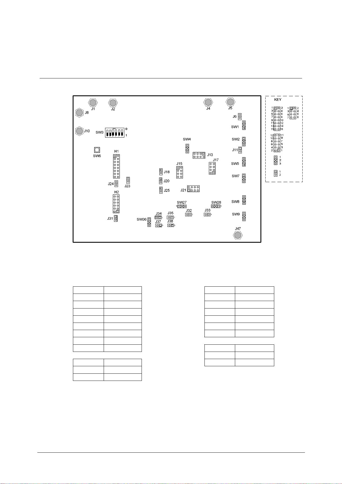
HEADERS .............................................................................................................. 7
LINKS, JUMPERS AND SWITCHES ...................................................................... 9
WM8750 OPERATION .................................................................................. 10
SOFTWARE CONTROL....................................................................................... 10
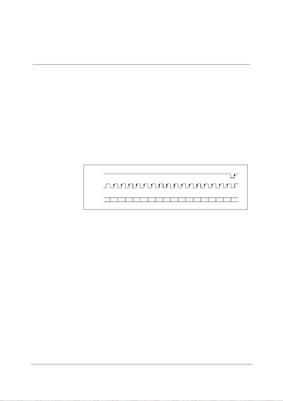
SERIAL INTERFACE SOFTWARE DESCRIPTION...................................... 13
SOFTWARE DOWNLOAD................................................................................... 13
SOFTWARE INSTALLATION............................................................................... 13
SOFTWARE OPERATION ................................................................................... 13
POWER DOWN AND INTERFACE CONTROL.................................................... 19
DAC AND ADC CONTROL................................................................................... 20
VOLUME CONTROL ............................................................................................ 21
MIXER CONTROL................................................................................................ 22
TONE CONTROL ................................................................................................. 23
SCHEMATIC LAYOUT .................................................................................. 24
WM8750-EV1B PCB LAYOUT...................................................................... 32
WM8750-EV1B BILL OF MATERIAL............................................................ 36
APPENDIX .................................................................................................... 38
EXTERNAL DSP CONNECTION TO THE WM8750-EV1B .......................... 38
AUDIO INTERFACE CONNECTIONS.................................................................. 38
SOFTWARE INTERFACE.................................................................................... 40
CONNECTION DIAGRAMS.................................................................................. 40
ADDITIONAL WM8750-EV1B SETUP RECOMMENDATIONS.................... 42
ADC TO DAC LOOPBACK................................................................................... 42
CONNECTION OF AN 8ΩMONO SPEAKER ...................................................... 44
HEADPHONE AUTO-DETECT FUNCTION ......................................................... 46

WM8750-EV1M
w Rev 2.0, February 2005
3
EVALUATION SUPPORT ............................................................................. 47
IMPORTANT NOTICE ................................................................................... 48
ADDRESS: ........................................................................................................... 48

WM8750-EV1M
w Rev 2.0, February 2005
4
INTRODUCTION
The WM8750 is a stereo CODEC for portable audio applications.
This evaluation platform and documentation should be used in conjunction with the latest
version of the WM8750 datasheet. The datasheet gives device functionality information as
well as timing and data format requirements.
This evaluation platform has been designed to allow the user ease of use and give optimum
performance in device measurement as well as providing the user with the ability to listen to
the excellent audio quality offered by the WM8750.
GETTING STARTED
EVALUATION BOARD CHECKLIST
The following items are available from Wolfson:
•WM8750-EV1B Evaluation Board - 6097_QFN32_EV1_REV1
•WM8750-EV1S Control Software (download from http://www.wolfsonmicro.com)
•WM8750-EV1M User Handbook (download from http://www.wolfsonmicro.com)
CUSTOMER REQUIREMENTS
Minimum customer requirements are:
•D.C. Power supply of +5V
•D.C. Power supply of +1.8V to +3.6V
•PC and printer cable (for software control)
Minimum PC spec requirements are:
•Win95/98/NT/2000/XP
•486 Processor
•Approximately 1.5Mb of free hard disk space
DAC Signal Path Requires:
•Digital coaxial or optical data source
•One set of active stereo speakers
ADC Signal Path Requires:
•Analogue coaxial or 3.5mm jack plug signal source
•Digital coaxial or optical data receiving unit
Analogue Signal Path Requires:
•Analogue coaxial or 3.5mm jack plug signal source
•One set of active stereo speakers

WM8750-EV1M
w Rev 2.0, February 2005
5
POWER SUPPLIES
Using appropriate power leads with 4mm connectors, power supplies should be connected
as described in Table 1.
REF-DES SOCKET NAME SUPPLY
J8 +5V +5V
J2 DBVDD +1.8V to +3.6V
J4 AVDD +1.8V to +3.6V
J10 DCVDD +1.42V to +3.6V
J47 HPVDD +1.8V to +3.6V
J1 DGND 0V
J5 AGND 0V
Table 1 Power Supply Connections
The DGND and AGND connections may be connected to a common GND on the supply with
no reduction in performance.
To reduce the supply connections that need to be attached to the EVB, sites L1 and L8 are
populated with 0R resistors shorting AVDD, HPVDD and DBVDD. In this configuration it is
recommended that the supply only be attached to AVDD. If separate supplies are required
the 0R resistors should be removed from sites L1 and L8.
Note: Refer to WM8750 datasheet for limitations on individual supply voltages.
Important: Exceeding the recommended maximum voltage can damage EVB
components. Under voltage may cause improper operation of some or all of the EVB
components.
BOARD FUNCTIONALITY
There are three options for inputting digital data into the WM8750 evaluation board. There is
a coaxial input (J19) via a standard phono connector or an optical input (U3) via a standard
optical receiver module. A direct digital input is also available via one side of a 2x8 pin
header (H1).
The analogue input signals are applied to the evaluation board via phono connectors J7
(RLINE_IN1), J12 (LLINE_IN1), J14 (RLINE_IN2), J22 (LLINE_IN2), J26 (RLINE_IN3) and
J45 (LLINE_IN3). Analogue inputs can also be applied to the evaluation board via 3.5mm
jack sockets J9 (MIC_IN1); J16 (MIC_IN2) and J30 (MIC_IN3).
There are two options for outputting digital data from the WM8750 evaluation board. There is
a coaxial output (J29) via a standard phono connector. The digital signals may also be
accessed via one side of a 2x8 pin header (H2).
The analogue outputs of the board are via phono connectors J43 (ROUT1), J44 (LOUT1),
J41 (LOUT2), J42 (ROUT2), J39 (MONO OUT) and J40 (OUT3). There is also an analogue
output via a 3.5mm jack socket J46 (HP_OUT).
All WM8750 device pins are accessible for easy measurement via the 2x4 pin headers (J13,
J15, J17 and J21) running up each side of the device.
Level-shift IC (U4) is used to shift the fixed +5V digital input from the CS8427 (U5) down to
the same level as DBVDD and vice-versa.

WM8750-EV1M
w Rev 2.0, February 2005
6
BOARD INPUT
REF-DES SOCKET NAME SIGNAL
J19 SPDIF_IN Digital (AES/EBU, UEC958,
S/PDIF, EIAJ CP340/1201)
signal.
U3 OPTICAL_IN Digital (AES/EBU, UEC958,
S/PDIF, EIAJ CP340/1201)
optical signal.
Table 2 Digital Inputs
REF-DES SOCKET NAME SIGNAL
J7 RLINE_IN1 Analogue signal
J12 LLINE_IN1 Analogue signal
J14 RLINE_IN2 Analogue signal
J22 LLINE_IN2 Analogue signal
J26 RLINE_IN3 Analogue signal
J45 LLINE_IN3 Analogue signal
J9 MIC_IN1 Analogue signal (MIC Input)
J16 MIC_IN2 Analogue signal (MIC Input)
J30 MIC_IN3 Analogue signal (MIC Input)
Analogue signals applied to these connectors are AC coupled before
being input to the WM8750.
Table 3 Analogue Inputs
Note: When used in Master Mode, an SPDIF signal must still be applied to phono connector
J19. This input signal is used to allow correct operation of the CS8427 as well as being used
to generate the MCLK for the WM8750.
BOARD OUTPUT
REF-DES SOCKET NAME SIGNAL
J29 SPDIF_OUT Digital (AES/EBU, UEC958,
S/PDIF, EIAJ CP340/1201)
signal.
Table 4 Digital Output
REF-DES SOCKET NAME SIGNAL
J43 ROUT1 Line/Headphone Output
J44 LOUT1 Line/Headphone Output
J42 ROUT2 Speaker Output
J41 LOUT2 Speaker Output
J39 MONO OUT Mono Output
J40 OUT3 ROUT1/VREF/MONO OUT
J46 HP_OUT Headphone Output
Table 5 Analogue Outputs

WM8750-EV1M
w Rev 2.0, February 2005
7
INTERFACES
11
1
111
11
1
1
1
1
1
1
1
1
Figure 1 Interfaces
HEADERS
H1 SIGNAL H2 SIGNAL
1/2 MCLK
12/11 GND
3/4 GND
10/9 ADCDAT
5/6 DACDAT
8/7 GND
7/8 GND
6/5 ADCLRC
9/10 DACLRC
4/3 GND
11/12 GND 2/1 BCLK
13/14 BCLK
15/16 GND J31 SIGNAL
1 DACLRC_OUT
J24 SIGNAL 2 GND
1 ADCLRC_IN
2 GND

WM8750-EV1M
w Rev 2.0, February 2005
8
J15 WM8750 PIN NAME J17 WM8750 PIN NAME
1 1 MCLK 1 17 HPVDD
2 2 DCVDD 2 18 AVDD
3 3 DBVDD 3 19 AGND
4 4 DGND 4 20 VREF
5 5 BCLK 5 21 VMID
6 6 DACDAT 6 22 MICBIAS
7 7 DACLRC 7 23 RINPUT3/HPDETECT
8 8 ADCDAT 8 24 LINPUT3
J21 WM8750 PIN NAME J13 WM8750 PIN NAME
1 9 ADCLRC 1 25 RINPUT2
2 10 MONOOUT 2 26 LINPUT2
3 11 OUT3 3 27 RINPUT1
4 12 ROUT1 4 28 LINPUT1
5 13 LOUT1 5 29 MODE
6 14 HPGND 6 30 CSB
7 15 ROUT2 7 31 SDIN
8 16 LOUT2 8 32 SCLK
Table 6 Headers

WM8750-EV1M
w Rev 2.0, February 2005
9
LINKS, JUMPERS AND SWITCHES
LINKS AND JUMPERS LINK/JUMPER STATUS DESCRIPTION
J18 (BCLK) OPEN
SHORT
Master mode
Slave mode [default setting]
J20 (ADCLRC) OPEN
SHORT
Master mode
Slave mode [default setting]
J25 (DACLRC) OPEN
SHORT
Master mode
Slave mode [default setting]
J23 OPEN
SHORT
Master mode
Slave mode (Ties ADCLRC to DACLRC) [default setting]
J32, J33, J34 and J35 OPEN
SHORT
OUT signals are AC coupled [default setting]
OUT signals are not AC coupled
J37 (external speaker connection) Pin 1 – AGND
Pin 2 – +ve speaker connection
J38 (external speaker connection) Pin 1 – AGND
Pin 2 – -ve speaker connection
J6 (DC input connection) Pin 1 – DC signal input
Pin 2 – AGND
J11 (DC input connection) Pin 1 – DC signal input
Pin 2 – AGND
Table 7 Links
SWITCHES SWITCH STATUS DESCRIPTION
SW6 After an input data format change has been made using
SW3, the CS8427 will only latch the new settings after
SW6 has been pressed and released.
SW3
(DATA FORMAT)
12 3 4 5 6 DATA FORMAT
1 0 0 1 0 0 I2S Compatible [default setting]
1 0 0 0 0 1 24-bit Right Justified
1 0 0 0 0 0 Left Justified
SW4
(Software Control)
Pins 1 and 2 SHORT
Pins 2 and 3 SHORT
3-wire (SPI) Control Mode [default setting]
2-wire Control Mode
SW1, SW2
(R/Line Input 1 Select)
Pins 1 and 2 SHORT
Pins 2 and 3 SHORT
MIC Input Select (3.5mm Jack Socket)
Line Input Select (Phono Socket) [default setting]
SW5, SW7
(R/Line Input 2 Select)
Pins 1 and 2 SHORT
Pins 2 and 3 SHORT
MIC Input Select (3.5mm Jack Socket)
Line Input Select (Phono Socket) [default setting]
SW8, SW9
(R/Line Input 3 Select)
Pins 1 and 2 SHORT
Pins 2 and 3 SHORT
MIC Input Select (3.5mm Jack Socket)
Line Input Select (Phono Socket) [default setting]
SW27, SW28
(R/LOUT 1 Select)
Pins 1 and 2 SHORT
Pins 2 and 3 SHORT
HP Output Select (3.5mm Jack Socket)
Line Output Select (Phono Socket) [default setting]
SW36 Pins 1 and 2 SHORT
Pins 2 and 3 SHORT
Connects to OUT3 for HP output DC reference
Connects to GND for HP output reference [default setting]
Table 8 Switches

WM8750-EV1M
w Rev 2.0, February 2005
10
WM8750 OPERATION
SOFTWARE CONTROL
There are two possible serial software control modes that may be selected to operate the
WM8750. The standard SPI user interface is a 3-wire solution with the second option being
a 2-wire solution.
3-WIRE MODE
To operate the WM8750 in SPI (3-wire) mode, jumper switch SW4 must be set so that pins
1 and 2 are SHORT. The 3-wire serial interface then becomes active on pins 30(CSB),
31(SDIN) and 32(SCLK). The serial interface on the board can be connected to a PC via the
printer port or any other standard parallel port. The port used can be selected through the
software provided. The software supplied with this kit gives the user access to all the
possible features provided by the WM8750. The 3-wire latch, data and clock lines may also
be connected to the board via the test points TP2 (CSB), TP4 (SDIN) and TP3 (SCLK).
Please refer to the WM8750 datasheet for full details of the serial interface timing and all
register features.
CSB
SCLK
SDIN B15 B6B7B8B9B10B11B12B13B14 B1B2B3B4B5 B0
Figure 2 3-Wire Serial Interface
2-WIRE MODE

WM8750-EV1M
w Rev 2.0, February 2005
11
To operate the WM8750 in 2-wire mode, jumper switch SW4 must be set so that pins 2 and
3 are SHORT. The 2-wire serial interface becomes active on pins 31(SDIN) and 32(SCLK).
The serial interface on the board can be connected to a PC via the printer port or any other
standard parallel port. Note: a bi-directional parallel port is required for 2-wire
operation1. The 2-wire data and clock lines may also be connected to the board via the test
points TP4 (SDIN) and TP3 (SCLK).
When used in 2-wire mode, the WM8750 has two possible addresses (0011010 [0x34h] or
0011011 [0x36h]) that are selectable by pulling CSB low or high. If connecting a probe to the
Test Points it must be noted that the CSB line is pulled high on the WM8750 evaluation
board selecting address 0011011. CSB must be pulled low or driven low through the software
writes if address 0011010 is used (as is done in the WM8750-EV1S software provided).
SDIN
SCLK
ACK
R ADDR ACK
DATA B15-8
STOPSTART
DATA B7-0R/W ACK
Figure 3 2-Wire Serial Interface
Note: 1If the 2-wire mode does not operate as expected, the likely cause is the configuration
of the parallel port interface mode. Check that the port is configured for bi-directional
communication. Most PCs allow the parallel port to be configured in the BIOS settings during
initial PC power up.

WM8750-EV1M
w Rev 2.0, February 2005
12
REGISTER
ADDRESS
(Bit 15 – 9)
remarks Bit[8] Bit[7] Bit[6] Bit[5] Bit[4] Bit[3] Bit[2] Bit[1] Bit[0] default
R0 (00h) 0000000 Left Input volume LIVU LINMUTE LIZC LINVOL 010010111
R1 (01h) 0000001 Right Input volume RIVU RINMUTE RIZC RINVOL 010010111
R2 (02h) 0000010 LOUT1 volume LO1VU LO1ZC LOUT1VOL[6:0] 001111001
R3 (03h) 0000011 ROUT1 volume RO1VU RO1ZC ROUT1VOL[6:0] 001111001
R4 (04h) 0000100 Reserved 0 0 0 0 0 0 0 0 0 000000000
R5 (05h) 0000101 ADC & DAC Control ADCDIV2 DACDIV2 ADCPOL[1:0] HPOR DACMU DEEMPH[1:0] ADCHPD 000001000
R6 (06h) 0000110 Reserved 0 0 0 0 0 0 0 0 0 000000000
R7 (07h) 0000111 Audio Interface 0 BCLKINV MS LRSWAP LRP WL[1:0] FORMAT[1:0] 000001010
R8 (08h) 0001000 Sample rate BCM[1:0] CLKDIV2 SR[4:0] USB 000000000
R9 (09h) 0001001 Reserved 0 0 0 0 0 0 0 0 0 000000000
R10 (0Ah) 0001010 Left DAC volume LDVU LDACVOL[7:0] 011111111
R11 (0Bh) 0001011 Right DAC volume RDVU RDACVOL[7:0] 011111111
R12 (0Ch) 0001100 Bass control 0 BB BC 0 0 BASS[3:0] 000001111
R13 (0Dh) 0001101 Treble control 0 0 TC 0 0 TRBL[3:0] 000001111
R15 (0Fh) 0001111 Reset writing to this register resets all registers to their default state not reset
R16 (10h) 0010000 3D control 0 MODE3D 3DUC 3DLC 3DDEPTH[3:0] 3DEN 000000000
R17 (11h) 0010001 ALC1 ALCSEL[1:0] MAXGAIN[2:0] ALCL[3:0] 001111011
R18 (12h) 0010010 ALC2 0 ALCZC 0 0 0 HLD[3:0] 000000000
R19 (13h) 0010011 ALC3 0 DCY[3:0] ATK[3:0] 000110010
R20 (14h) 0010100 Noise Gate 0 NGTH[4:0] NGG[1:0] NGAT 000000000
R21 (15h) 0010101 Left ADC volume LAVU LADCVOL[7:0] 011000011
R22 (16h) 0010110 Right ADC volume RAVU RADCVOL[7:0] 011000011
R23 (17h) 0010111 Additional control(1) TSDEN VSEL[1:0] DMONOMIX[1:0] DATSEL[1:0] DACINV TOEN 011000000
R24 (18h) 0011000 Additional control(2) OUT3SW[1:0] HPSWEN
HPSWPOL
ROUT2INV
TRI LRCM ADCOSR DACOSR 000000000
R25 (19h) 0011001 Pwr Mgmt (1) VMIDSEL[1:0] VREF AINL AINR ADCL ADCR MICB DIGENB 000000000
R26 (1Ah) 0011010 Pwr Mgmt (2) DACL DACR LOUT1 ROUT1 LOUT2 ROUT2 MONO OUT3 0 000000000
R27 (1Bh) 0011011 Additional Control (3) ADCLRM[1:0] VROI 0 0 0 0 0 0 000000000
R31 (1Fh) 0011111 ADC input mode DS MONOMIX[1:0] RDCM LDCM 0 0 0 0 000000000
R32 (20h) 0100000 ADCL signal path 0 LINSEL[1:0] LMICBOOST[1:0] 0 0 0 0 000000000
R33 (21h) 0100001 ADCR signal path 0 RINSEL[1:0] RMICBOOST[1:0] 0 0 0 0 000000000
R34 (22h) 0100010 Left out Mix (1) LD2LO LI2LO LI2LOVOL[2:0] 0 LMIXSEL[2:0] 001010000
R35 (23h) 0100011 Left out Mix (2) RD2LO RI2LO RI2LOVOL[2:0] 0 0 0 0 001010000
R36 (24h) 0100100 Right out Mix (1) LD2RO LI2RO LI2ROVOL[2:0] 0 RMIXSEL[2:0] 001010000
R37 (25h) 0100101 Right out Mix (2) RD2RO RI2RO RI2ROVOL[2:0] 0 0 0 0 001010000
R38 (26h) 0100110 Mono out Mix (1) LD2MO LI2MO LI2MOVOL[2:0] 0 0 0 0 001010000
R39 (27h) 0100111 Mono out Mix (2) RD2MO RI2MO RI2MOVOL[2:0] 0 0 0 0 001010000
R40 (28h) 0101000 LOUT2 volume LO2VU LO2ZC LOUT2VOL[6:0] 001111001
R41 (29h) 0101001 ROUT2 volume RO2VU RO2ZC ROUT2VOL[6:0] 001111001
R42 (2Ah) 0101010 MONOOUT volume 0 MOZC MOUTVOL[6:0] 001111001
Table 9 Mapping of Program Registers
Please refer to the WM8750 datasheet for full details of the serial interface timing and all
register features.

WM8750-EV1M
w Rev 2.0, February 2005
13
SERIAL INTERFACE SOFTWARE DESCRIPTION
The following section will detail the downloading and installation of evaluation software and
also the operation of the software and the functionality of each control button.
SOFTWARE DOWNLOAD
The current evaluation board control software WM8750-EV1S should be downloaded from
the Wolfson website [www.wolfsonmicro.com].
From the homepage it is recommended to carry out a search for ‘WM8750’ and select the
evaluation board ’more’ button. Select ‘download’ from the top right hand corner under the
software label. Once the licence agreement has been accepted, select the
WM8750_EV1S_REVx.x.ZIP link and download to your hard drive.
SOFTWARE INSTALLATION
Once the .zip file has been downloaded, to install the software:
•Open the .zip file.
•Double click on the setup.exe file.
•Follow the on-screen installation instructions and save to the desired location.
The software can then be opened by either running the extracted WM8750_EV1_REVx.x.exe
file from the saved location or alternatively, selecting: Start > Programs > WM8750-EV1S-
REVx.x > WM8750-EV1S.
SOFTWARE OPERATION
Due to the many features offered by the WM8750, the software has been split into five
different panels. This eases the complexity of the software making each panel less busy, the
panels have also been grouped so that it makes it simple to control each section of the
device.
The main menu panel shown in Figure 4 is used to call up the other panels as well as
offering a number of pull-down menus.
Figure 4 Software Menu Panel

WM8750-EV1M
w Rev 2.0, February 2005
14
The ‘Submit All’ button will submit values to every register of the WM8750. The ‘Reset’
button writes to the reset register (R15) but does not reset the control panel values. If the
previous values are to be resubmitted then the ‘Submit All’ button should be pressed, if the
user would like to start afresh then the ‘Reset Software Panel Settings’ button should also be
pressed. Pressing this button does not write to the device, it only resets the panel settings to
their default state. Left clicking on the Wolfson logo will open the PCs default web browser
and go to the Wolfson Microelectronics website (‘www.wolfsonmicro.com’). The DAC, ADC
and Line setup buttons have also been provided as a quick start approach. Pressing either of
these buttons will power up the DAC, ADC or Line signal paths in a known state as described
in the following pages.
Important: The CS8427 SPDIF decoder IC will only work at a rate of 256fs. This will limit
the sample rates that may be set using the WM8750 unless an external source is used to
supply signals directly to the relevant pins of header H1 or taking the signals from the
relevant pins of header H2.
DAC SUBMIT SETUP
By pressing the ‘DAC Setup’ button, the software writes to the device setting the following
path: SPDIF_In through the DAC to the L/ROUT1 and L/ROUT2 outputs. The default format
setting is 24-bit, I2S. Table 6 lists the required board settings to allow this signal path to be
used. This button is intended to ease the initial use of the WM8750 until the user becomes
familiar with both device and software operation.
Figure 5 Recommended DAC Setup

WM8750-EV1M
w Rev 2.0, February 2005
15
LINKS AND
JUMPERS
LINK/JUMPER STATUS DESCRIPTION
H1 All jumpers in place DAC clocks and data input
H2 No jumpers in place ADC clocks and data output
SW36 Pins 2 and 3 SHORT Connects to GND for HP output reference
J18 (BCLK) SHORT Slave mode
J20 (ADCLRC) SHORT Slave mode
J25 (DACLRC) SHORT Slave mode
J23 SHORT Slave mode
J32, J33, J34 and
J35
OPEN OUT signals are AC coupled
SW3 12 3 4 5 6 DATA FORMAT
1 0 0 1 0 0 I2S Compatible
SW4 Pins 1 and 2 SHORT 3-wire (SPI) Control Mode
SW1, SW2 Pins 2 and 3 SHORT Line Input Select (Phono Socket)
SW5, SW7 Pins 2 and 3 SHORT Line Input Select (Phono Socket)
SW8, SW9 Pins 2 and 3 SHORT Line Input Select (Phono Socket)
SW27, SW28 Pins 2 and 3 SHORT Line Output Select (Phono Socket)
Table 10 DAC Setup Jumper Settings (Slave Mode)
ADC SUBMIT SETUP
By pressing the ‘ADC Setup’ button, the software writes to the device setting the
L/RLINE_IN1 through ADC to SPDIF_Out path active. As with the DAC setup described
previously, this is to ease the initial use of the WM8750 until the user becomes familiar with
both device and software operation. It should be noted that the SPDIF_In connection is still
required to provide the necessary clocks to the WM8750 in this mode.
Figure 6 Recommended ADC Setup

WM8750-EV1M
w Rev 2.0, February 2005
16
LINKS AND
JUMPERS
LINK/JUMPER STATUS DESCRIPTION
H1 All jumpers in place
except for the jumper
connecting pins 5 and 6
and 7 and 8.
DAC clocks and data input
H2 All jumpers in place ADC clocks and data output
SW36 Pins 2 and 3 SHORT Connects to GND for HP output reference
J18 (BCLK) SHORT Slave mode
J20 (ADCLRC) SHORT Slave mode
J25 (DACLRC) SHORT Slave mode
J23 SHORT Slave mode
J32, J33, J34 and
J35
OPEN OUT signals are AC coupled
SW3 12 3 4 5 6 DATA FORMAT
1 0 0 1 0 0 I2S Compatible
SW4 Pins 1 and 2 SHORT 3-wire (SPI) Control Mode
SW1, SW2 Pins 2 and 3 SHORT Line Input Select (Phono Socket)
SW5, SW7 Pins 2 and 3 SHORT Line Input Select (Phono Socket)
SW8, SW9 Pins 2 and 3 SHORT Line Input Select (Phono Socket)
SW27, SW28 Pins 2 and 3 SHORT Line Output Select (Phono Socket)
Table 11 ADC Setup Jumper Setup (Slave Mode)

WM8750-EV1M
w Rev 2.0, February 2005
17
LINE SUBMIT SETUP
By pressing the ‘Line Setup’ button, the software writes to the device setting the
L/RLINE_IN1 through the analogue path to the L/ROUT1 and L/ROUT2 outputs. As with the
setups previously described, this is to ease the initial use of the WM8750 until the user
becomes familiar with both device and software operation.
H1
J2
SW3
SW6
J5
J1 J4
0
1
J15 J17
J13
J21
PARALLEL PORT
12 3456
OPEN
AGND
AVDD
+1.8V
to
+3.6V
DGND
DBVDD
+1.8V
to
+3.6V
MONO
OUT
OUT3
LOUT2
ROUT2
RLINE
IN1
LLINE
IN1
RLINE -
IN2
LLINE
IN2
RLINE
IN3
LLINE
IN3
OPT
_IN
SPDIF_
IN
SPDIF_
OUT
H2
J8
+5V
J10
DCVDD
+1.42V
to
+3.6V
J47
HPVDD
+1.8V
to
+3.6V
J24
1
J31
1
J23
1
J20
1
J25
1
J18
1
J37
1
J34
1
J38
1
J35
1
J32
1
J33
1
J6
1
J11
1
SW1
1
1
SW2
SW5
1
1
SW7
SW8
1
1
SW9
1
SW36
1SW27 SW281
1
SW4
ROUT1
LOUT1
Figure 7 Recommended Line Setup

WM8750-EV1M
w Rev 2.0, February 2005
18
LINKS AND JUMPERS LINK/JUMPER STATUS DESCRIPTION
H1 No jumpers in place DAC clocks and data input
H2 No jumpers in place ADC clocks and data output
SW36 Pins 2 and 3 SHORT Connects to GND for HP output reference
J18 (BCLK) SHORT Slave mode
J20 (ADCLRC) SHORT Slave mode
J25 (DACLRC) SHORT Slave mode
J23 SHORT Slave mode
J32, J33, J34 and J35 OPEN OUT signals are AC coupled
SW3 12 3 4 5 6 DATA FORMAT
1 0 0 1 0 0 I2S Compatible
SW4 Pins 1 and 2 SHORT 3-wire (SPI) Control Mode
SW1, SW2 Pins 2 and 3 SHORT Line Input Select (Phono Socket)
SW5, SW7 Pins 2 and 3 SHORT Line Input Select (Phono Socket)
SW8, SW9 Pins 2 and 3 SHORT Line Input Select (Phono Socket)
SW27, SW28 Pins 2 and 3 SHORT Line Output Select (Phono Socket)
Table 12 Line Setup Jumper Setup (Slave Mode)

WM8750-EV1M
w Rev 2.0, February 2005
19
POWER DOWN AND INTERFACE CONTROL
Figure 8 Power and Interface Control
The Power Down and Interface Control panel is used to enable/disable the various sections
of the WM8750. It is also used to set the audio interface to the required data format.
Pressing the ‘Power Submit’ button will cause the settings shown on this panel to be written
to the WM8750. A full device register write is not sent.

WM8750-EV1M
w Rev 2.0, February 2005
20
DAC AND ADC CONTROL
Figure 9 DAC and ADC Control
The DAC and ADC Control panel is used to control the many DAC and ADC related features
of the WM8750. Pressing the ‘ADC and DAC Submit’ button will cause the settings shown on
this panel to be written to the WM8750. A full device register write is not sent.
Table of contents
Other Wolfson Motherboard manuals

Wolfson
Wolfson WM8766-EV1M Instruction Manual

Wolfson
Wolfson WM832 Series User manual

Wolfson
Wolfson WM8716 Quick start guide

Wolfson
Wolfson WM8761-EV1M Instruction Manual

Wolfson
Wolfson WM8778-EV1B Instruction Manual

Wolfson
Wolfson WM8973-EV1B Instruction Manual

Wolfson
Wolfson WM8738 Instruction Manual

Wolfson
Wolfson WM8510-EV1M Instruction Manual