Wolfson WM8766-EV1M Instruction Manual

w WM8766-EV1M
WM8766 Evaluation Board User Handbook
WOLFSO MICROELECTRO ICS plc
www.wolfsonmicro.com
November 2003, Rev 1.2
Copyright 2003 Wolfson Microelectronics plc
I TRODUCTIO
The WM 766 is a 24-bit, 192kHz 6-Channel DAC.
This evaluation platform and documentation should be used in conjunction with the latest version of
the WM 766 datasheet. The datasheet gives device functionality information as well as timing and
data format requirements.
This evaluation platform has been designed to allow the user ease of use and give optimum
performance in device measurement as well as providing the user with the ability to listen to the
excellent audio quality offered by the WM 766.
GETTI G STARTED
PACKI G LIST
The WM 766 Evaluation Kit contains:
• 1 WM 766-EV1B Evaluation Board
• 2 WM 766-EV1S 3.5” floppy disks containing control software
• This manual -1 WM 766-EV1M
CUSTOMER REQUIREME TS
Minimum customer requirements are:
• D.C. Power supply of +12V and -12V
• D.C. Power supply of +2.7V to +5.5V
• PC and printer cable (for software control)
Minimum spec requirements are:
• Win95/9 /NT/2000/XP
• 4 6 Processor
DAC Signal Path Requires:
• Digital coaxial or optical data source
• 1 set of active stereo speakers

WM8766-EV1M
w
Rev 1.2 November 2003
2
EVALUATION BOARD OPERATION
POWER SUPPLIES
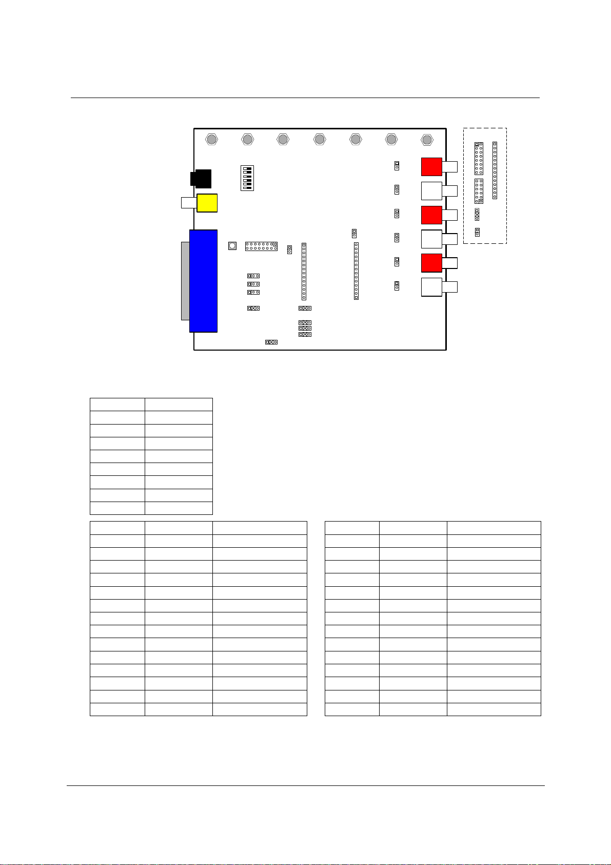
Using appropriate power leads with 4mm connectors, supplies should be connected as described in
Table 1.
REF-DES SOCKET NAME SUPPLY
1 +5V +5V
3 DVDD +2.7V to +3.6V
4 AVDD +2.7V to +5.5V
6 -12V -12V
7 +12V +12V
2 DGND 0V
5 AGND 0V
Table 1 Po er Supply Connections
The DGND and AGND connections may be connected to a common GND on the supply with no
reduction in performance.
Note:
Refer to WM8766 datasheet for limitations on individual supply voltages.
Important: Exceeding the recommended maximum voltage can damage EVB components.
Under voltage may cause improper operation of some or all of the EVB components.
BOARD FUNCTIONALITY
There are three options for inputting digital data into the WM8766 evaluation board. There is a
coaxial input ( 10) via a standard phono connector or an optical input (U1) via a standard optical
receiver module. A direct digital input is also available via one side of a 2x8 pin header (H1).
The analogue outputs of the board are via phono connectors 21 (VOUT2R), 28 (VOUT2L), 14
(VOUT3R), 18 (VOUT3L), 9 (VOUT4R), 12 (VOUT4L).
All WM8766 device pins are accessible for easy measurement via the 1x14 pin headers ( 16 and
25) running up each side of the device.
Level-shift IC (U7) is used to shift the fixed +5V digital input from the CS8427 (U3) down to the same
level as DVDD and vice-versa.
BOARD INPUT
When used in Slave Mode digital clock signals must be applied to the WM8766. A digital (AES/EBU,
UEC958, S/PDIF, EIA CP340/1201) signal input may be applied to the coaxial input ( 10), or the
optical input (U1), allowing the CS8427 (U3) to generate the necessary clocks. A direct digital input
is also available via one side of a 2x8 pin header (H1) data must be input in one of the WM8766
supported formats - see datasheet.
Note:
When used in Master Mode, an SPDIF signal must still be applied to phono connector 10. This
input signal is used to allow correct operation of the CS8427 as well as being used to generate the
MCLK for the WM8766.
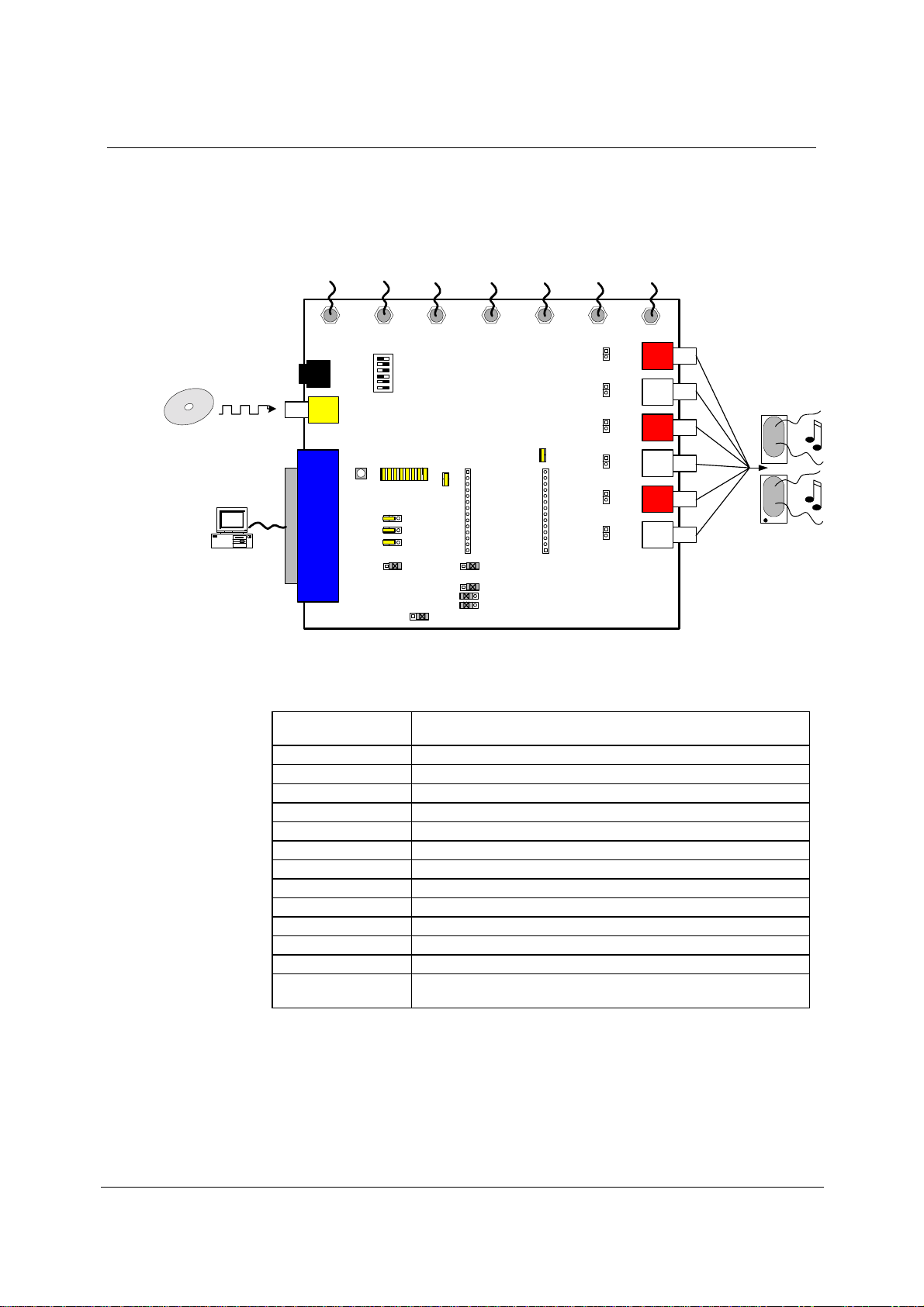
BOARD OUTPUT
The WM8766 eval board can also be used with the 8 channel WM8768. As a result, the board has
decals for 4 stereo channels (VOUT1-4). Since the WM8766 provides 3 stereo channels, VOUT1L/R
are left unpopulated on the board. Instead, VOUT1L/R of the chip are output on VOUT2L/R of the
eval board. Similarly, VOUT2L/R and VOUT3L/R of the chip are output on VOUT3L/R and
VOUT4L/R of the board respectively (see Table 5).
There are 6 analogue signal output phono connectors starting at VOUT2L/R: 21 (VOUT2R), 28
(VOUT2L), 14 (VOUT3R), 18 (VOUT3L), 9 (VOUT4R) and 12 (VOUT4L). Each of these outputs
is passed through a post DAC active low-pass filter.

WM8766-EV1M
w
Rev 1.2 November 2003
3
I TERFACES
KEY
1
2
3
H1
J2
SW1
SW2
1
3
5
7
9
11
13
15
2
4
6
10
12
14
16
1
2
J3 J5 J6 J7
J1 J4
LNK2
J15
1
J19
J
1
J11
1
J13
1
J17
1
J20
1
J27
1
1
3
5
7
9
11
2
4
6
10
12
J16
J25
1
2
3
4
5
6
7
9
10
11
12
13
14
1234 5 6
OPEN
01
1
1
1
1
1
1
1
1
1
1
LNK1
LNK7
LNK6
LNK5
LNK4
J22
J23
J24
VOUT2L
VOUT2R
VOUT3L
VOUT4L
VOUT3R
VOUT4R
Figure 1 Interfaces
HEADERS
H1 SIG AL
1/2 DACDAT
3/4 GND
5/6 DACLRC
7/ GND
9/10 DACBCLK
11/12 GND
13/14 DACMCLK_IN
15/16 GND
J16 WM8766 PI AME J19 WM8766 PI AME
1 1 MODE 1 15 TESTREF
2 2 MCLK 2 16 VREFN
3 3 BCLK 3 17 VREFP
4 4 LRCLK 4 1 VMID
5 5 DVDD 5 19 NC
6 6 DGND 6 20 NC
7 7 DIN1 7 21 VOUT1L
DIN2 22 VOUT1R
9 9 DIN3 9 23 VOUT2L
10 10 DNC 10 24 VOUT2R
11 11 ML/I2S 11 25 VOUT3L
12 12 MC/IWL 12 26 VOUT3R
13 13 MD/DM 13 27 AGND
14 14 MUTE 14 2 AVDD
Table 2 Headers

WM8766-EV1M
w
Rev 1.2 November 2003
4
LI KS
LI KS A D JUMPERS DESCRIPTIO
LNK1 (Master/Slave) Pins 1 and 2 SHORT – Master Mode
Pins 2 and 3 SHORT – Slave Mode
LNK2 (Mute) Pins 1 and 2 SHORT – MUTE On
Pins 2 and 3 SHORT – MUTE Off
LNK4 (MD/DM) Pins 1 and 2 SHORT – DEEMPH Activated
Pins 2 and 3 SHORT – DEEMPH De-activated
LNK7 (MODE) Pins 1 and 2 SHORT – Hardware Mode
Pins 2 and 3 SHORT – Software Mode
LNK6 (MC/IWL)
[Hardware Mode Only]
LNK5 (ML/I2S)
[Hardware Mode Only]
LNK6 LNK5 FORMAT
2-3 2-3 24-bit Right Justified
2-3 1-2 20-bit Right Justified
1-2 2-3 16-bit I2S
1-2 1-2 24-bit I2S
J15 (AVDD) OPEN - No Power to AVDD (used for current measurements)
SHORT - Power to AVDD
J19 (DVDD) OPEN - No Power to DVDD (used for current measurements)
SHORT - Power to DVDD
J22 Pins 1 and 2 SHORT – Connect DIN1 to DACDAT
Pins 2 and 3 SHORT – Connect DIN1 to GND
J23 Pins 1 and 2 SHORT – Connect DIN2 to DACDAT
Pins 2 and 3 SHORT – Connect DIN2 to GND
J24 Pins 1 and 2 SHORT – Connect DIN3 to DACDAT
Pins 2 and 3 SHORT – Connect DIN3 to GND
J , J11, J13, J17, J20, J27 OPEN - VOUT signals are AC coupled before the LPF
SHORT - VOUT signals are not AC coupled before the LPF
Table 3 Links
SWITCHES
SWITCH DESCRIPTIO
SW2 After an input data format change has been made using SW2, the CS 427 will
only latch the new settings after SW1 has been pressed and released.
SW1
(DATA
FORMAT)
1 2 3 4 5 6 DATA FORMAT
1 0 0 1 0 0 I2S Compatible
1 0 0 0 0 1 24-bit Right Justified
1 0 0 0 0 0 Left Justified
Table 4 Switches
A ALOGUE OUTPUTS
CHIP BOARD
VOUT1L/R VOUT2L/R
VOUT2L/R VOUT3L/R
VOUT3L/R VOUT4L/R
Table 5 Analogue Outputs

WM8766-EV1M
w
Rev 1.2 November 2003
5
WM8766 OPERATIO
HARDWARE MODE
To operate the WM 766 in hardware mode, the jumper on link LNK7 (MODE) must short pins 1 and
2 together. The 3-pin links on the board (LNK1, 2, 4, 5, 6) then become the active source for
changing the device functions. The diagram shown in Figure 2 used with the settings specified in
Table 6 will assist in setting the WM 766-EV1B into a known state. This is to ease the initial use of
the WM 766 until the user becomes familiar with device operation.
H1
J2
SW1
SW2
J3 J5 J6 J7
J1 J4
LNK2
J15
1
J19
J
1
J11
1
J13
1
J17
1
J20
1
J27
1
J16
J25
1234 5 6
OPEN
01
1
1
1
1
1
1
1
1
1
1
LNK1
LNK7
LNK6
LNK5
LNK4
J22
J23
J24
VOUT2L
VOUT2R
VOUT3L
VOUT4L
VOUT3R
VOUT4R
+5V DGND
+2.7V
to
+3.6V -12V +12V
AGND
+2.7V
to
+5.5V
Figure 2 Recommended DAC Setup
LI KS A D
JUMPERS
DESCRIPTIO
H1 All jumpers in place
LNK1 (Master/Slave) Pins 2 and 3 SHORT - Slave Mode
LNK2 (MUTE) Pins 2 and 3 SHORT – MUTE off
LNK4 (MD/DM) Pins 2 and 3 SHORT – No De-emphasis
LNK7 (MODE) Pins 1 and 2 SHORT – Hardware Mode
LNK6 (MC/IWL)
LNK5 (ML/I2S)
LNK6 LNK5 FORMAT
1-2 1-2 24-bit I2S
J15 (AVDD) SHORT - Power to AVDD
J19 (DVDD) SHORT - Power to DVDD
J22 Pins 1 and 2 SHORT – Connect DIN1 to DACDAT
J23 Pins 1 and 2 SHORT – Connect DIN2 to DACDAT
J24 Pins 1 and 2 SHORT – Connect DIN3 to DACDAT
J , J11, J13, J17, J20,
J27
OPEN - VOUT signals are AC coupled before the LPF
Table 6 DAC Hardware Jumper Setup (Slave Mode)
Please refer to Table 3 of this document and the WM 766 datasheet for further details on device
configuration in hardware mode.

WM8766-EV1M
w
Rev 1.2 November 2003
6
SOFTWARE CO TROL
To operate the WM 766 in SPI (3-wire) software mode, the jumper on link LNK7 (MODE) must short
pins 2 and 3 together. The SPI interface then becomes active on device pins 11(ML/I2S),
12(MC/IWL) and 13(MD/DM). The serial interface on the board can be connected to a PC via the
printer port or any other standard parallel port. The port used can be selected through the software
provided. The software supplied with this kit gives the user access to all the possible features
provided by the WM 766.
Please refer to the WM 766 datasheet for full details of the serial interface timing.
ML/I2S
MC/IWL
MD/DM
B15 B6B7B8B9B10B11B12B13B14 B1 B2 B3 B4B5 B0
Figure 3 SPI Serial Interface
REGISTER B15 B14 B13 B12 B11 B10 B9 B B7 B6 B5 B4 B3 B2 B1 B0 DEFAULT
R0(00h) 0 0 0 0 0 0 0 UPDATE LDA1[7:0] 011111111
R1(01h) 0 0 0 0 0 0 1 UPDATE RDA1[7:0] 011111111
R2(02h) 0 0 0 0 0 1 0 PL[ :5] IZD ATC
PDWN
All DAC
DEEMP
ALL DAC
MUTE
All DAC
100100000
R3(03h) 0 0 0 0 0 1 1 PHASE[ :6] DACIWL[5:4] DACBCP DACLRP DACFMT[1:0] 000000000
R4(04h) 0 0 0 0 1 0 0 UPDATE LDA2[7:0] 011111111
R5(05h) 0 0 0 0 1 0 1 UPDATE RDA2[7:0] 011111111
R6(06h) 0 0 0 0 1 1 0 UPDATE LDA3[7:0] 011111111
R7(07h) 0 0 0 0 1 1 1 UPDATE RDA3[7:0] 011111111
R (0 h) 0 0 0 1 0 0 0 UPDATE MASTDA[7:0] 011111111
R9(09h) 0 0 0 1 0 0 1 DEEMP[ :6] DMUTE[5:3] DZFM[2:1] ZCD 000000000
R10(0Ah) 0 0 0 1 0 1 0 DACRATE[ :6] DACMS PWRDN
ALL
DACD[3:1] 0 010000000
R12(0Ch) 0 0 0 1 1 0 0 0 0 MPD 0 0 0 0 0 0 000000000
R15(0Fh) 0 0 0 1 1 1 1 0 0 0 MPD 0 0 0 0 0 00000000
R31(1Fh) 0 0 1 1 1 1 1 RESET 000000000
Table 7 Mapping of Program Registers
Please refer to the WM 766 datasheet for full details of the register features.
Important: It must be noted that the CS 427 SPDIF decoder IC will only work at a rate of 256fs. This
will limit the sample rates that may be set using the WM 766 unless an external source is used
supplying signals directly to the relevant pins of header H1.

WM8766-EV1M
w
Rev 1.2 November 2003
7
SERIAL I TERFACE SOFTWARE DESCRIPTIO
SOFTWARE I STALLATIO
There are 2 floppy disks supplied with this evaluation kit. To install the software:
1. Insert disk 1
2. Select the ‘Start’ button on the Windows task bar and the ‘Run…’ option.
3. Type “A:\setup” and then press OK.
4. Follow the on-screen instructions
SOFTWARE OPERATIO
The WM 766 software can be configured for use with the WM 796, WM 79 and WM 76 . Select
the WM 766 in the drop down menu labelled ‘Select device’.
Due to the many features offered by the WM 766 the software has been split into 3 different panels.
This eases the complexity of the software making each panel less busy, the panels have also been
grouped so that it makes it simple to control each section of the device.
The main menu panel shown in Figure 4 is used to call up the other panels as well as offering a
number of pull-down menus.
Figure 4 Software Menu Panel

WM8766-EV1M
w
Rev 1.2 November 2003
The ‘Submit’ button will submit values to every register of the WM 766. The ‘Device Reset’ button
writes to the reset register R31 but does not reset the control panel values. If the previous values are
to be resubmitted then the ‘Submit’ button should be pressed, if the user would like to start afresh
then the ‘Reset Software Panel Settings’ button should also be pressed. Pressing this button does
not write to the device, it only resets the panel settings to their default state. Left clicking on the
Wolfson logo will open the PCs default web browser and go top the Wolfson Microelectronics
website (‘www.wolfsonmicro.com’).
Pressing the ‘Submit Master Control’ button will only submit changes made to the Master Power
Down switch.
WRITI G TO REGISTERS
Two methods are provided to write to the WM 766 registers:
1. By pressing buttons ‘DAC SETUP CONTROL’ and ‘DAC VOLUME CONTROL’ on the software
menu panel (Figure 4), further panels control will open (see Figure 6 and Figure 7). These
panels display sliders and buttons that provide a visual interface to the registers of the
WM 766. For example when the volume sliders for DAC1 on the DAC VOLUME CONTROL
panel are used, they update the settings in registers R0 and R1 accordingly.
2. On the software control panel itself, there is a map of all registers and their current settings.
Registers can be directly set from this panel.
Any changes made in the ‘DAC SETUP CONTROL’ and ‘DAC VOLUME CONTROL’ panels will be
reflected in the register map on the software control panel and vice versa.

WM8766-EV1M
w
Rev 1.2 November 2003
9
TEST SETUP FOR STA DARD DAC OPERATIO
For the standard ‘DAC Setup’ the device is setup to receive data via the SPDIF_In to the DAC, after
conversion the DAC outputs to VOUT1/2/3. Table lists the required board settings to allow this
signal path to become active in 24-bit, I2S input data format. This is to ease the initial use of the
WM 766 until the user becomes familiar with both device and software operation.
H1
J2
SW1
SW2
J3 J5 J6 J7
J1 J4
LNK2
J15
1
J19
J
1
J11
1
J13
1
J17
1
J20
1
J27
1
J16
J25
1234 5 6
OPEN
01
1
1
1
1
1
1
1
1
1
1
LNK1
LNK7
LNK6
LNK5
LNK4
J22
J23
J24
VOUT2L
VOUT2R
VOUT3L
VOUT4L
VOUT3R
VOUT4R
+5V DGND
+2.7V
to
+3.6V -12V +12V
AGND
+2.7V
to
+5.5V
Figure 5 Recommended DAC Setup
LI KS A D
JUMPERS
DESCRIPTIO
H1 All jumpers in place
LNK1 (Master/Slave) Pins 2 and 3 SHORT - Slave Mode
LNK2 (MUTE) Pins 2 and 3 SHORT – MUTE off
LNK4 (MD/DM) No Effect
LNK7 (MODE) Pins 2 and 3 SHORT – Software Mode
LNK6 (MC/IWL) No Effect
LNK5 (ML/I2S) No Effect
J15 (AVDD) SHORT - Power to AVDD
J19 (DVDD) SHORT - Power to DVDD
J22 Pins 1 and 2 SHORT – Connect DIN1 to DACDAT
J23 Pins 1 and 2 SHORT – Connect DIN2 to DACDAT
J24 Pins 1 and 2 SHORT – Connect DIN3 to DACDAT
J , J11, J13, J17, J20,
J27
OPEN - VOUT signals are AC coupled before the LPF
Table 8 DAC Software Jumper Setup (Slave Mode)

WM8766-EV1M
w
Rev 1.2 November 2003
10
DAC CO TROL
Figure 6 DAC Control
The DAC Control panel is used to control the many DAC related features of the WM 766. Pressing
the ‘DAC Submit’ button will cause the settings shown on this panel to be written to the WM 766. A
full device register write is not sent.

WM8766-EV1M
w
Rev 1.2 November 2003
11
DAC ATTE UATIO CO TROL
Figure 7 DAC Attenuation Control
The DAC Attenuation Control panel is used to control both the digital DAC volume of the WM 766.
The volume sliders update in ‘real’ time (i.e. the ‘DAC Attenuation Submit’ button does not have to be
pressed to update the output volume level) but will only have an effect on the output if the
UPDATEL/R bits are set. Once changes are made to the UPDATEL/R bits, the ‘DAC Attenuation
Submit’ button must be left clicked for the change to take effect. Pressing the ‘DAC Attenuation
Submit’ button will cause the settings shown on this panel to be written to the WM 766. A full device
register write is not sent.

WM8766-EV1M
w
Rev 1.2 November 2003
12
WM8766-EV1B SCHEMATIC
Figure 8 Functional Diagram
Figure 9 SPDIF Input / Output Interface

WM8766-EV1M
w
Rev 1.2 November 2003
13
Figure 10 Software Control
Figure 11 Level Shift

WM8766-EV1M
w
Rev 1.2 November 2003
14
Figure 12 WM8766

WM8766-EV1M
w
Rev 1.2 November 2003
15
Figure 13 Analogue Output

WM8766-EV1M
w
Rev 1.2 November 2003
16
Figure 14 Power

WM8766-EV1M
w
Rev 1.2 November 2003
17
WM8766-EV1B PCB LAYOUT
Figure 15 Top Layer Silkscreen

WM8766-EV1M
w
Rev 1.2 November 2003
1
Figure 16 Top Layer

WM8766-EV1M
w
Rev 1.2 November 2003
19
Figure 17 Bottom Layer

WM8766-EV1M
w
Rev 1.2 November 2003
20
Figure 18 Bottom Layer Silkscreen
Table of contents
Other Wolfson Motherboard manuals

Wolfson
Wolfson WM832 Series User manual

Wolfson
Wolfson WM8510-EV1M Instruction Manual

Wolfson
Wolfson WM8778-EV1B Instruction Manual

Wolfson
Wolfson WM8738 Instruction Manual

Wolfson
Wolfson WM8761-EV1M Instruction Manual

Wolfson
Wolfson WM8750-EV1M Instruction Manual

Wolfson
Wolfson WM8716 Quick start guide

Wolfson
Wolfson WM8973-EV1B Instruction Manual