Wolfson WM8580 User manual

wWM8580
Multichannel CODEC with S/PDIF Transceiver
WOLFSON MICROELECTRONICS plc
To receive regular email updates, sign up at http://www.wolfsonmicro.com/enews/
Production Data, March 2009, Rev 4.7
Copyright ©2009 Wolfson Microelectronics plc
DESCRIPTION
The WM8580 is a multi-channel audio CODEC with S/PDIF
transceiver. The WM8580 is ideal for DVD and surround
sound processing applications for home hi-fi, automotive
and other audiovisual equipment.
Integrated into the device is a stereo 24-bit multi-bit sigma
delta ADC with support for digital audio output word lengths
from 16-bit to 32-bit, and sampling rates from 8kHz to
192kHz.
Also included are three stereo 24-bit multi-bit sigma delta
DACs, each with a dedicated oversampling digital
interpolation filter. Digital audio input word lengths from 16-
bits to 32-bits and sampling rates from 8kHz to 192kHz are
supported. Each DAC channel has independent digital
volume and mute control.
Two independent audio data interfaces support I2S, Left
Justified, Right Justified and DSP digital audio formats.
Each audio interface can operate in either Master Mode or
Slave Mode.
The S/PDIF transceiver is IEC-60958-3 compatible and
supports frame rates from 32k/s to 96k/s. It has four
multiplexed inputs and one output. Status and error
monitoring is built-in and results can reported over the serial
interface or via GPO pins. S/PDIF Channel Block
configuration is also supported.
The device has two PLLs that can be configured
independently to generate two system clocks for internal or
external use.
Device control and setup is via a 2-wire or 3-wire (SPI
compatible) serial interface. The serial interface provides
access to all features including channel selection, volume
controls, mutes, de-emphasis, S/PDIF control/status, and
power management facilities. Alternatively, the device has a
Hardware Control Mode where device features can be
enabled/disabled using selected pins.
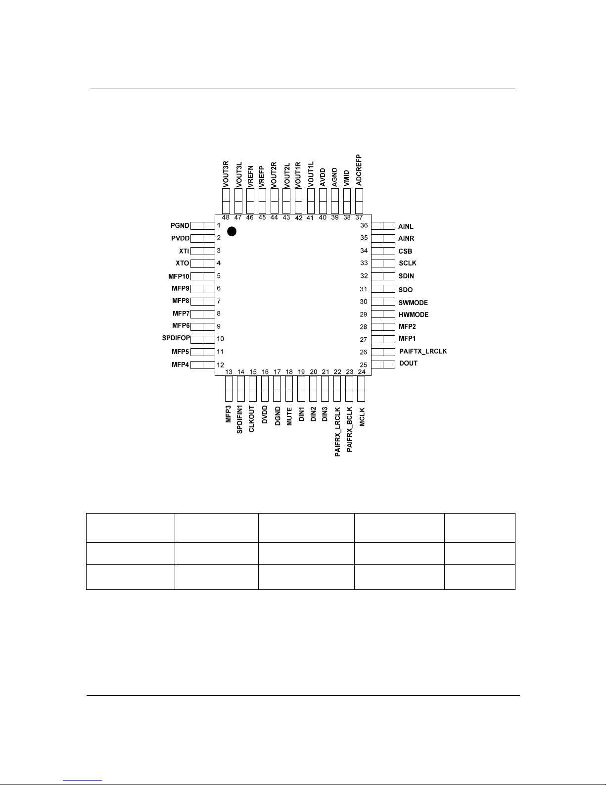
The device is available in a 48-lead TQFP package.
FEATURES
•Multi-channel CODEC with 3 Stereo DACs and 1 Stereo
ADC
•Integrated S/PDIF / IEC-60958-3 transceiver
•Audio Performance
−103dB SNR (‘A’ weighted @ 48kHz) DAC
−-90dB THD (48kHz) DAC
−100dB SNR (‘A’ weighted @ 48kHz) ADC
−-87dB THD (48kHz) ADC
•DAC Sampling Frequency: 8kHz – 192kHz
•ADC Sampling Frequency: 8kHz – 192kHz
•Independent ADC and DAC Sample Rates
•2 and 3-Wire Serial Control Interface with readback, or
Hardware Control Interface
•GPO pins allow visibility of user selected status flags
•Programmable Audio Data Interface Modes
−I
2S, Left, Right Justified or DSP
−16/20/24/32 bit Word Lengths
•Three Independent Stereo DAC Outputs with Digital
Volume Controls
•Two Independent Master or Slave Audio Data Interfaces
•Flexible Digital Interface Routing with Clock Selection
Control
•2.7V to 5.5V Analogue, 2.7V to 3.6V Digital Supply
Operation
•48-lead TQFP Package
APPLICATIONS
•Digital TV
•DVD Players and Receivers
•Surround Sound AV Processors and Hi-Fi systems
•Automotive Audio
Downloaded from Elcodis.com electronic components distributor

Production Data WM8580
w PD, Rev 4.7, March 2009
3
TABLE OF CONTENTS
DESCRIPTION .......................................................................................................1
FEATURES.............................................................................................................1
APPLICATIONS .....................................................................................................1
BLOCK DIAGRAM .................................................................................................2
TABLE OF CONTENTS .........................................................................................3
PIN CONFIGURATION...........................................................................................4
ORDERING INFORMATION ..................................................................................4
PIN DESCRIPTION ................................................................................................5
MULTI-FUNCTION PINS............................................................................................... 6
ABSOLUTE MAXIMUM RATINGS.........................................................................8
RECOMMENDED OPERATING CONDITIONS .....................................................9
ELECTRICAL CHARACTERISTICS ......................................................................9
TERMINOLOGY .......................................................................................................... 12
MASTER CLOCK TIMING........................................................................................... 12
DIGITAL AUDIO INTERFACE – MASTER MODE....................................................... 13
DIGITAL AUDIO INTERFACE – SLAVE MODE .......................................................... 14
CONTROL INTERFACE TIMING – 3-WIRE MODE .................................................... 15
CONTROL INTERFACE TIMING – 2-WIRE MODE .................................................... 16
DEVICE DESCRIPTION.......................................................................................17
INTRODUCTION......................................................................................................... 17
CONTROL INTERFACE OPERATION........................................................................ 18
DIGITAL AUDIO INTERFACES................................................................................... 22
AUDIO DATA FORMATS ............................................................................................ 24
AUDIO INTERFACE CONTROL.................................................................................. 28
DAC FEATURES......................................................................................................... 30
ADC FEATURES......................................................................................................... 39
DIGITAL ROUTING OPTIONS .................................................................................... 40
CLOCK SELECTION................................................................................................... 42
PHASE-LOCKED LOOPS AND S/PDIF CLOCKING (SOFTWARE MODE)................ 53
PHASE-LOCKED LOOPS AND S/PDIF CLOCKING (HARDWARE MODE) ............... 60
S/PDIF TRANSCEIVER............................................................................................... 60
POWERDOWN MODES ............................................................................................. 73
INTERNAL POWER ON RESET CIRCUIT.................................................................. 75
HARDWARE CONTROL MODE.................................................................................. 77
REGISTER MAP ......................................................................................................... 81
DIGITAL FILTER CHARACTERISTICS ...............................................................96
DAC FILTER RESPONSES......................................................................................... 97
DIGITAL DE-EMPHASIS CHARACTERISTICS........................................................... 98
ADC FILTER RESPONSES......................................................................................... 98
ADC HIGH PASS FILTER ........................................................................................... 99
APPLICATIONS INFORMATION .......................................................................100
RECOMMENDED EXTERNAL COMPONENTS........................................................ 100
PACKAGE DIMENSIONS ..................................................................................102
IMPORTANT NOTICE ........................................................................................103
ADDRESS: ................................................................................................................ 103
Downloaded from Elcodis.com electronic components distributor

WM8580 Production Data
w PD, Rev 4.7, March 2009
4
PIN CONFIGURATION
ORDERING INFORMATION
DEVICE TEMPERATURE
RANGE PACKAGE MOISTURE
SENSITIVITY LEVEL
PEAK
SOLDERING
TEMPERATURE
WM8580AGEFT/V -40 to +85oC 48-lead TQFP
(Pb-free) MSL2 260°C
WM8580AGEFT/RV -40 to +85oC 48-lead TQFP
(Pb-free, tape and reel) MSL2 260°C
Note:
Reel quantity = 2,200
Downloaded from Elcodis.com electronic components distributor

Production Data WM8580
w PD, Rev 4.7, March 2009
5
PIN DESCRIPTION
PIN NAME TYPE DESCRIPTION
1 PGND Supply PLL ground
2 PVDD Supply PLL positive supply
3 XTI Digital Input Crystal or CMOS clock input
4 XTO Digital Output Crystal output
5 MFP10 Digital Output Multi-Function Pin (MFP) 10. See Table 1 for details of all MFP pins.
6 MFP9 Digital Output Multi-Function Pin (MFP) 9. See Table 1 for details of all MFP pins.
7 MFP8 Digital Input/Output Multi-Function Pin (MFP) 8. See Table 1 for details of all MFP pins.
8 MFP7 Digital Input/Output Multi-Function Pin (MFP) 7. See Table 1 for details of all MFP pins.
9 MFP6 Digital Input/Output Multi-Function Pin (MFP) 6. See Table 1 for details of all MFP pins.
10 SPDIFOP Digital Output S/PDIF transmitter output.
11 MFP5 Digital Input/Output Multi-Function Pin (MFP) 5. See Table 1 for details of all MFP pins.
12 MFP4 Digital Input/Output Multi-Function Pin (MFP) 4. See Table 1 for details of all MFP pins.
13 MFP3 Digital Input/Output Multi-Function Pin (MFP) 3. See Table 1 for details of all MFP pins.
14 SPDIFIN1 Digital Input S/PDIF receiver input 1
15 CLKOUT Digital Output PLL or crystal oscillator clock output
16 DVDD Supply Digital positive supply
17 DGND Supply Digital ground
18 MUTE Digital Input/Output DAC mute-all Input / All-DAC Infinite Zero Detect (IZD) flag output
19 DIN1 Digital Input Primary Audio Interface (PAIF) receiver data input 1
20 DIN2 Digital Input Primary Audio Interface (PAIF) receiver data input 2
21 DIN3 Digital Input Primary Audio Interface (PAIF) receiver data input 3
22 PAIFRX_LRCLK Digital Input/Output Primary Audio Interface (PAIF) receiver left/right word clock
23 PAIFRX_BCLK Digital Input/Output Primary Audio Interface (PAIF) receiver bit clock
24 MCLK Digital Input/Output System Master clock; 256, 384, 512, 768, 1024 or 1152 fs
25 DOUT Digital Output Primary Audio Interface (PAIF) transmitter data output
26 PAIFTX_LRCLK Digital Input/Output Primary audio interface transmitter left/right word clock
27 MFP1 Digital Input/Output Multi-Function Pin (MFP) 1. See Table 1 for details of all MFP pins.
28 MFP2 Digital Input/Output Multi-Function Pin (MFP) 2. See Table 1 for details of all MFP pins.
29 HWMODE Digital Input Configures control to be either Software Mode or Hardware Mode
30 SWMODE Digital Input/Output Configures software interface to be either 2-wire or 3-wire. See note 2.
31 SDO Digital Output 3-wire control interface data output. See note 3.
32 SDIN Digital Input/Output Control interface data input (and output under 2-wire control)
33 SCLK Digital Input Control interface clock
34 CSB Digital Input 3-wire control interface latch signal / device address selection
35 AINR Analogue Input ADC Right Channel Input
36 AINL Analogue Input ADC Left Channel Input
37 ADCREFP Analogue Output ADC reference buffer decoupling pin; 10uF external decoupling
38 VMID Analogue Output Midrail divider decoupling pin; 10uF external decoupling
39 AGND Supply Analogue ground
40 AVDD Supply Analogue positive supply
41 VOUT1L Analogue Output DAC channel 1 left output
42 VOUT1R Analogue Output DAC channel 1 right output
43 VOUT2L Analogue Output DAC channel 2 left output
44 VOUT2R Analogue Output DAC channel 2 right output
45 VREFP Analogue Input DAC and ADC positive reference
46 VREFN Analogue Input DAC and ADC ground reference
Downloaded from Elcodis.com electronic components distributor

WM8580 Production Data
w PD, Rev 4.7, March 2009
6
PIN NAME TYPE DESCRIPTION
47 VOUT3L Analogue Output DAC channel 3 left output
48 VOUT3R Analogue Output DAC channel 3 right output
Notes :
1. Digital input pins have Schmitt trigger input buffers. Pins 32, 33, 34 are 5V tolerant.
2. In hardware control mode, pin 30 is used for UNLOCK flag output.
3. In hardware control mode, pin 31 is used for NON_AUDIO flag output.
MULTI-FUNCTION PINS
The WM8580 has 8 Multi-Function Input/Output pins (MFP1 etc.). The function and direction (input/output) of these pins
are configured using the HWMODE input pin and software register control as shown below. If HWMODE is set, the MFPs
have the function shown in column 1 of Table 1. If HWMODE is not set, and the register SAIF_EN is set, the MFPs have
the function shown in column 2. Otherwise, the GPOnOP registers determine the MFP function as shown in columns 3 and
4.
PIN NAME HARDWARE
CONTROL MODE
FUNCTION
1
SECONDARY AUDIO
INTERFACE FUNCTION
2
S/PDIF INPUT &
INDEPENDENT
CLOCKING
3
GENERAL PURPOSE
OUTPUT FUNCTION
4
MFP1 PAIFTX_BCLK n/a1PAIFTX_BCLK2GPO1
MFP2 ADCMCLK n/a1ADCMCLK3GPO2
MFP3 DR1 n/a1SPDIFIN2 GPO3
MFP4 DR2 n/a1SPDIFIN3 GPO4
MFP5 DR3 n/a1SPDIFIN4 GPO5
MFP6 DR4 SAIF_BCLK GPO6 GPO6
MFP7 ALLPD SAIF_LRCLK GPO7 GPO7
MFP8 C SAIF_DIN GPO8 GPO8
MFP9 SFRM_CLK SAIF_DOUT GPO9 GPO9
MFP10 192BLK n/a1GPO10 GPO10
Table 1 Multi-Function Pin Configuration
Notes:
1. These pins are not used as part of the Secondary Audio Interface, so their function is that of either Column 3 or
Column 4.
2. MFP1 usage can be described as follows:
IF (ADC_CLKSEL = MCLK) AND (PAIFTXMS_CLKSEL = MCLK) THEN
MFP1 = GPO1;
ELSE
MFP1 = PAIFTX_BCLK ; (default)
HWMODE = 1
GPIOnOP
SAIF_EN = 1
Y
Y
N
N
Downloaded from Elcodis.com electronic components distributor

Production Data WM8580
w PD, Rev 4.7, March 2009
7
Notes for MFP1:
ADC_CLKSEL selected in REG 8, default is ADC_MCLK.
PAIFTXMS_CLKSEL selects PLLACLK if PAIF sources SPDIF Rx, otherwise PAIFTXMS_CLKSEL selects ADC_CLK
(register 8)
3. MFP2 usage can be described as follows:
IF (ADC_CLKSEL ≠ADCMCLK) (controlled by reg 8)
AND (TX_CLKSEL ≠ADCMCLK) (controlled by reg 8)
AND (SAIFMS_CLKSEL ≠ADCMCLK) THEN (controlled by reg 8)
MFP2 = GPO2;
ELSE
MFP2 = ADCMCLK;
PIN FUNCTION TYPE DESCRIPTION
PAIFTX_BCLK Digital Input/Output Primary Audio Interface Transmitter (PAIFTX) Bit Clock
ADCMCLK Digital Input Master ADC clock; 256fs, 384fs, 512fs ,786fs, 1024fs or 1152fs
SAIF_DIN Digital Input Secondary Audio Interface (SAIF) Receiver data input
SAIF_DOUT Digital Output Secondary Audio Interface (SAIF) Transmitter data output
SAIF_BCLK Digital Input/Output Secondary Audio Interface (SAIF) Bit Clock
SAIF_LRCLK Digital Input/Output Secondary Audio Interface (SAIF) Left/Right Word Clock
SPDIFIN2/3/4 Digital Input S/PDIF Receiver Input
GPO1 – GPO10 Digital Output General Purpose Output
DR1/2/3/4 Digital Input Internal Digital Routing Configuration in Hardware Mode
ALLPD Digital Input Chip Powerdown in Hardware Mode
C Digital Output Recovered channel-bit for current S/PDIF sub-frame
SFRM_CLK Digital Output Indicates current S/PDIF sub-frame:
1 = Sub-frame A
0 = Sub-frame B
192BLK Digital Output Indicates start of S/PDIF 192-frame block. High for duration of frame 0.
Table 2 Multi-Function Pin Description
Downloaded from Elcodis.com electronic components distributor

WM8580 Production Data
w PD, Rev 4.7, March 2009
8
ABSOLUTE MAXIMUM RATINGS
Absolute Maximum Ratings are stress ratings only. Permanent damage to the device may be caused by continuously operating at
or beyond these limits. Device functional operating limits and guaranteed performance specifications are given under Electrical
Characteristics at the test conditions specified.
ESD Sensitive Device. This device is manufactured on a CMOS process. It is therefore generically susceptible
to damage from excessive static voltages. Proper ESD precautions must be taken during handling and storage
of this device.
The WM8580 has been classified as MSL1, which has an unlimited floor life at <30oC / 85% Relative Humidity and therefore will
not be supplied in moisture barrier bags.
CONDITION MIN MAX
Digital supply voltage -0.3V +3.63V
Analogue supply voltage -0.3V +7V
PLL supply voltage -0.3V +5.5V
Voltage range digital inputs (SCLK, CSB & SDIN only) DGND -0.3V +7V
Voltage range digital inputs DGND -0.3V DVDD + 0.3V
Voltage range analogue inputs 1AGND -0.3V
PGND -0.3V
AVDD +0.3V
PVDD +0.3V
Master Clock Frequency 37MHz
Operating temperature range -40°C +85°C
Storage temperature prior to soldering 30°C max / 85% RH max
Storage temperature after soldering -65°C +150°C
Pb Free Package body temperature (soldering 10 seconds) +260°C
Package body temperature (soldering 2 minutes) +183°C
Notes: 1. Analogue and digital grounds must always be within 0.3V of each other.
Downloaded from Elcodis.com electronic components distributor

Production Data WM8580
w PD, Rev 4.7, March 2009
9
RECOMMENDED OPERATING CONDITIONS
PARAMETER SYMBOL TEST CONDITIONS MIN TYP MAX UNIT
Digital supply range DVDD 2.7 3.6 V
Analogue supply range AVDD 2.7 5.5 V
PLL supply range PVDD 4.5 5.5 V
Ground
A
GND, VREFN, DGND.
PGND
0 V
Difference DGND to
AGND/PGND
-0.3 0 +0.3 V
Note: Digital supply DVDD must never be more than 0.3V greater than AVDD.
ELECTRICAL CHARACTERISTICS
Test Conditions
AVDD, PVDD, VREFP = 5V, DVDD = 3.3V, AGND, VREFN = 0V, PGND, DGND = 0V, TA = +25oC, 1kHz Signal, fs = 48kHz, 24-
Bit Data, Slave Mode, MCLK, ADCMCLK = 256fs, 1Vrms Input Signal Level unless otherwise stated.
PARAMETER SYMBOL TEST CONDITIONS MIN TYP MAX UNIT
DAC Performance (Load = 10kΩ, 50pF) WM8580AGEFT/V, WM8580AGEFT/RV (+25˚C)
0dBFs Full scale output voltage -6% 1.0 x
VREFP/5
+6% Vrms
A-weighted,
@ fs = 48kHz
95 103 dB
Unweighted,
@ fs = 48kHz
100 dB
A-weighted,
@ fs = 48kHz, AVDD =
3.3V
99 dB
A-weighted,
@ fs = 96kHz
101 dB
Unweighted,
@ fs = 96kHz
98 dB
A-weighted,
@ fs = 96kHz, AVDD =
3.3V
99 dB
A-weighted,
@ fs = 192kHz
101 dB
Unweighted,
@ fs = 192kHz
98 dB
Signal to Noise Ratio (See
Terminology 1,2,4)
SNR
A-weighted,
@ fs = 192kHz, AVDD
= 3.3V
99 dB
Dynamic Range (See
Terminology 2,4)
DNR A-weighted, -60dB full
scale input
95 103 dB
1
kHz, 0dB Full Scale @
fs = 48kHz
-90 -85 dB
1
kHz, 0dB Full Scale @
fs = 96kHz
-87 dB
Total Harmonic Distortion THD
1
kHz, 0dB Full Scale @
fs = 192kHz
-84 dB
DAC Channel separation 100 dB
Mute Attenuation 1kHz Input, 0dB gain 100 dB
Output Offset Error 2 mV
Downloaded from Elcodis.com electronic components distributor

WM8580 Production Data
w PD, Rev 4.7, March 2009
10
Test Conditions
AVDD, PVDD, VREFP = 5V, DVDD = 3.3V, AGND, VREFN = 0V, PGND, DGND = 0V, TA = +25oC, 1kHz Signal, fs = 48kHz, 24-
Bit Data, Slave Mode, MCLK, ADCMCLK = 256fs, 1Vrms Input Signal Level unless otherwise stated.
PARAMETER SYMBOL TEST CONDITIONS MIN TYP MAX UNIT
1kHz 100mVp-p 50 dB
Power Supply Rejection Ratio
(See note 4)
PSRR
20Hz to 20kHz
100mVp-p
45 dB
ADC Performance WM8580AGEFT/V, WM8580AGEFT/RV (+25˚C)
Full Scale Input Signal Level (for
ADC 0dB Input)
1.0 x
VREFP/5
V
rms
Input resistance 6 kΩ
Input capacitance 10 pF
A-weighted,
@ fs = 48kHz
90 100 dB
Unweighted,
@ fs = 48kHz
97 dB
A-weighted,
@ fs = 48kHz, AVDD =
3.3V
97 dB
A-weighted,
@ fs = 96kHz
97 dB
Unweighted,
@ fs = 96kHz
94 dB
A-weighted,
@ fs = 96kHz, AVDD =
3.3V
94 dB
A-weighted,
@ fs = 192kHz
97 dB
Unweighted,
@ fs = 192kHz
94 dB
Signal to Noise Ratio (See
Terminology 1,2,4)
SNR
A-weighted,
@ fs = 192kHz, AVDD
= 3.3V
94 dB
1kHz, -1dB Full Scale
@ fs = 48kHz
-87 -80 dB
1kHz, -1dB Full Scale
@ fs = 96kHz
-86 dB
Total Harmonic Distortion THD
1kHz, -1dB Full Scale
@ fs = 192kHz
-85 dB
Dynamic Range DNR -60dB FS 90 100
ADC Channel Separation 1kHz Input 97 dB
Channel Level Matching (See
Terminology 4)
1KHz Signal 0.1 dB
Channel Phase Deviation 1kHz Signal 0.0001 Degree
Offset Error HPF On
HPF Off
0
100
LSB
LSB
Digital Logic Levels (CMOS Levels)
Input LOW level VIL 0.3 x DVDD V
Input HIGH level VIH 0.7 x DVDD V
Input leakage current -1 ±0.2 +1 µA
Input capacitance 5 pF
Output LOW VOL IOL=1mA 0.1 x DVDD V
Output HIGH VOH IOH=-1mA 0.9 x DVDD V
Downloaded from Elcodis.com electronic components distributor

Production Data WM8580
w PD, Rev 4.7, March 2009
11
Test Conditions
AVDD, PVDD, VREFP = 5V, DVDD = 3.3V, AGND, VREFN = 0V, PGND, DGND = 0V, TA = +25oC, 1kHz Signal, fs = 48kHz, 24-
Bit Data, Slave Mode, MCLK, ADCMCLK = 256fs, 1Vrms Input Signal Level unless otherwise stated.
PARAMETER SYMBOL TEST CONDITIONS MIN TYP MAX UNIT
Analogue Reference Levels
Reference voltage VVMID VREFP/2 –
50mV
VREFP/2 VREFP/2 +
50mV
V
VREFP to VMID and
VMID to VREFN
VMIDSEL = 1
14 kΩ
Potential divider resistance RVMID
VREFP to VMID and
VMID to VREFN
VMIDSEL = 0
44 kΩ
S/PDIF Transceiver Performance
Jitter on recovered clock 50 ps
S/PDIF Input Levels CMOS MODE
Input LOW level VIL 0.3 X DVDD V
Input HIGH level VIH 0.7 X DVDD V
Input capacitance 1.25 pF
Input Frequency 36 MHz
S/PDIF Input Levels Comparator MODE
Input capacitance 10 pF
Input resistance 23 kΩ
Input frequency 25 MHz
Input Amplitude 200 0.5 X DVDD mV
PLL
Period Jitter 80 ps(rms)
XTAL
Input XTI LOW level VXIL 0 557 mV
Input XTI HIGH level VXIH 853 mV
Input XTI capacitance CXJ 3.32 4.491 pF
Input XTI leakage IXleak 28.92 38.96 mA
Output XTO LOW VXOL 15pF load capacitors 86 278 mV
Output XTO HIGH VXOH 15pF load capacitors 1.458 1.942 V
Supply Current
Analogue supply current AVDD, VREFP = 5V 45 mA
Analogue supply current AVDD, VREFP = 3.3V 30 mA
Digital supply current DVDD = 3.3V 25 mA
Power Down 500 µA
Notes:
1. Ratio of output level with 1kHz full scale input, to the output level with all zeros into the digital input, measured ‘A’
weighted.
2. All performance measurements done with 20kHz low pass filter, and where noted an A-weight filter. Failure to use
such a filter will result in higher THD+N and lower SNR and Dynamic Range readings than are found in the Electrical
Characteristics. The low pass filter removes out of band noise; although it is not audible, it may affect dynamic
specification values.
3. VMID decoupled with 10uF and 0.1uF capacitors (smaller values may result in reduced performance).
4. PSSR measured with VMID set to high impedance
Downloaded from Elcodis.com electronic components distributor

WM8580 Production Data
w PD, Rev 4.7, March 2009
12
TERMINOLOGY
1. Signal-to-noise ratio (dB) - SNR is a measure of the difference in level between the full scale output and the output
with no signal applied. (No Auto-zero or Automute function is employed in achieving these results).
2. Dynamic range (dB) - DNR is a measure of the difference between the highest and lowest portions of a signal.
Normally a THD+N measurement at 60dB below full scale. The measured signal is then corrected by adding the 60dB
to it. (e.g. THD+N @ -60dB= -32dB, DR= 92dB).
3. THD (dB) - THD is a ratio, of the rms values, of Distortion/Signal.
4. Stop band attenuation (dB) - Is the degree to which the frequency spectrum is attenuated (outside audio band).
5. Channel Separation (dB) - Also known as Cross-Talk. This is a measure of the amount one channel is isolated from
the other. Normally measured by sending a full scale signal down one channel and measuring the other.
6. Pass-Band Ripple - Any variation of the frequency response in the pass-band region.
MASTER CLOCK TIMING
ADCMCLK/
MCLK
t
MCLKL
tMCLKH
t
MCLKY
Figure 1 Master Clock Timing Requirements
Test Conditions
AVDD, PVDD, VREFP = 5V, DVDD = 3.3V, AGND, VREFN = 0V, PGND, DGND = 0V, TA = +25oC
PARAMETER SYMBOL TEST CONDITIONS MIN TYP MAX UNIT
System Clock Timing Information
ADCMCLK and MCLK System clock
pulse width high
tMCLKH 11 ns
ADCMCLK and MCLK System clock
pulse width low
tMCLKL 11 ns
ADCMCLK and MCLK System clock
cycle time
tMCLKY 28 ns
ADCMCLK and MCLK Duty cycle 40:60 60:40
Table 3 Master Clock Timing Requirements
Downloaded from Elcodis.com electronic components distributor

Production Data WM8580
w PD, Rev 4.7, March 2009
13
DIGITAL AUDIO INTERFACE – MASTER MODE
PAIFRX_BCLK/
PAIFTX_BCLK/
SAIF_BCLK
(Output)
DOUT/
SAIF_DOUT
PAIFRX_LRCLK/
PAIFTX_LRCLK/
SAIF_LRCLK
(Outputs)
tDL
DIN1/2/3
SAIF_DIN
tDDA
tDHT
tDST
Figure 2 Digital Audio Data Timing – Master Mode
Test Conditions
AVDD, PVDD, VREFP = 5V, DVDD = 3.3V, AGND, VREFN, PGND, DGND = 0V, TA = +25oC, Master Mode, fs = 48kHz, MCLK
and ADCMCLK = 256fs unless otherwise stated.
PARAMETER SYMBOL TEST CONDITIONS MIN TYP MAX UNIT
Audio Data Input Timing Information
PAIFTX_LRCLK/
PAIFRX_LRCLK/
SAIF_LRCLK propagation
delay from PAIFTX_BCLK/
PAIFRX_BCLK/
SAIF_BCLK falling edge
tDL 0 10 ns
DOUT/SAIF_DOUT
propagation delay from
PAIFTX_BCLK/
SAIF_BCLK falling edge
tDDA 0 10 ns
DIN1/2/3/SAIF_DIN setup
time to
PAIFRX_BCLK/SAIF_BCLK
rising edge
tDST 10 ns
DIN1/2/3/SAIF_DIN hold
time from
PAIFRX_BCLK/SAIF_BCLK
rising edge
tDHT 10 ns
Table 4 Digital Audio Data Timing – Master Mode
Downloaded from Elcodis.com electronic components distributor

WM8580 Production Data
w PD, Rev 4.7, March 2009
14
DIGITAL AUDIO INTERFACE – SLAVE MODE
PAIFTX_BCLK/
PAIFRX_BCLK/
SAIF_BCLK
PAIFTX_LRCLK/
PAIFRX_LRCLK/
SAIF_BCLK
DIN1/2/3/
SAIF_DIN
DOUT/
SAIF_DOUT
tBCH tBCL
tBCY
tLRSU
tDS tLRH
tDH
tDD
Figure 3 Digital Audio Data Timing – Slave Mode
Test Conditions
AVDD, PVDD = 5V, DVDD = 3.3V, AGND = 0V, PGND,DGND = 0V, TA = +25oC, Slave Mode, fs = 48kHz, MCLK and
ADCMCLK = 256fs unless otherwise stated.
PARAMETER SYMBOL TEST CONDITIONS MIN TYP MAX UNIT
Audio Data Input Timing Information
PAIFTX_BCLK/
PAIFRX_BCLK/SAIF_BCLK cycle
time
tBCY 50 ns
PAIFTX_BCLK/
PAIFRX_BCLK/SAIF_BCLK pulse
width high
tBCH 20 ns
PAIFTX_BCLK/
PAIFRX_BCLK/SAIF_BCLK pulse
width low
tBCL 20 ns
PAIFTX_LRCLK/
PAIFRX_LRCLK/SAIF_BCLK set-up
time to PAIFTX_BCLK/
PAIFRX_BCLK/SAIF_BCLK rising
edge
tLRSU 10 ns
PAIFTX_LRCLK/
PAIFRX_LRCLK/
SAIF_LRCLK hold time from
PAIFTX_BCLK/
PAIFRX_BCLK/SAIF_BCLK rising
edge
tLRH 10 ns
DIN1/2/3/SAIF_DIN set-up time to
PAIFRX_BCLK/
SAIF_BCLK rising edge
tDS 10 ns
DIN1/2/3/SAIF_DIN hold time from
PAIFRX_BCLK/SAIF_BCLK rising
edge
tDH 10 ns
DOUT/SAIF_DOUT propagation
delay from
PAIFTX_BCLK/SAIF_BCLK falling
edge
tDD 0 10 ns
Table 5 Digital Audio Data Timing – Slave Mode
Downloaded from Elcodis.com electronic components distributor

Production Data WM8580
w PD, Rev 4.7, March 2009
15
CONTROL INTERFACE TIMING – 3-WIRE MODE
CSB
SCLK
SDIN
tDHO
tDSU
tCSH
tSCY tSCS
LSB
SDO
tDL
LSB
tCSS
tCSU
tCSM
Figure 4 SPI Compatible Control Interface Input Timing
Test Conditions
AVDD, PVDD = 5V,DVDD = 3.3V, AGND, PGND,DGND = 0V, TA = +25oC, fs = 48kHz, MCLK and ADCMCLK = 256fs unless
otherwise stated
PARAMETER SYMBOL MIN TYP MAX UNIT
SCLK rising edge to CSB rising edge tSCS 60 ns
SCLK pulse cycle time tSCY 80 ns
SCLK duty cycle 40/60 60/40 ns
SDIN to SCLK set-up time tDSU 20 ns
SDIN hold time from SCLK rising edge tDHO 20 ns
SDO propagation delay from SCLK falling
edge
tDL 5 ns
CSB pulse width high tCSH 20 ns
SCLK to CSB low (required for read cycle)
set-up time
tCSU 20 ns
CSB min (write cycle only) tCSM 0.5* tSCY ns
CSB rising/falling to SCLK rising tCSS 20 ns
SCLK glitch suppression tps 2 8 ns
Table 6 3-Wire SPI Compatible Control Interface Input Timing Information
Downloaded from Elcodis.com electronic components distributor

WM8580 Production Data
w PD, Rev 4.7, March 2009
16
CONTROL INTERFACE TIMING – 2-WIRE MODE
Figure 5 Control Interface Timing – 2-Wire Serial Control Mode
Test Conditions
AVDD, PVDD = 5V,DVDD = 3.3V, AGND, PGND,DGND = 0V, TA = +25oC, fs = 48kHz, MCLK and ADCMCLK = 256fs unless
otherwise stated
PARAMETER SYMBOL MIN TYP MAX UNIT
Program Register Input Information
SCLK Frequency 0 526 kHz
SCLK Low Pulse-Width t11.3 us
SCLK High Pulse-Width t2600 ns
Hold Time (Start Condition) t3600 ns
Setup Time (Start Condition) t4600 ns
Data Setup Time t5100 ns
SDIN, SCLK Rise Time t6300 ns
SDIN, SCLK Fall Time t7300 ns
Setup Time (Stop Condition) t8600 ns
Data Hold Time t9900 ns
SCLK glitch suppression tps 0 5 ns
Table 7 2-Wire Control Interface Timing Information
t
3
t
1
t6
t9
t
2
t5
t7
t3
t4t8
SDIN
SCLK
Downloaded from Elcodis.com electronic components distributor

Production Data WM8580
w PD, Rev 4.7, March 2009
17
DEVICE DESCRIPTION
INTRODUCTION
WM8580 is a complete mutli-channel CODEC with integrated S/PDIF transceiver. The device
comprises three separate stereo DACs and a stereo ADC, in a single package, and controlled by
either software or hardware interfaces.
The three stereo DAC outputs are ideal to implement a complete 5.1 channel surround system. Each
DAC has its own digital volume control (adjustable in 0.5dB steps) with zero cross detection. With
zero cross enabled, volume updates occur as a signal transitions through its zero point. This
minimises audible clicks and ‘zipper’ noise as the gain values change.
Each stereo DAC has its own data input (DIN1/2/3) and shared word clock (PAIFRX_LRCLK), bit
clock (PAIFRX_BCLK) and master clock (MCLK). The stereo ADC has data output (DOUT), word
clock (PAIFTX_LRCLK), and bit clock (PAIFTX_BCLK). This allows the ADC to operate at a different
sample rate to the DACs. In addition, a separate ADC master clock (ADCMCLK) can be used instead
of MCLK for further flexibility.
There are two independent Digital Audio Interfaces, which may be configured to operate in either
master or slave mode. In Slave mode, the LRCLKs and BCLKs are inputs. In Master mode, the
LRCLKs and BCLKs are outputs.
The Audio Interfaces support Right Justified, Left Justified, I2S and DSP formats. Word lengths of 16,
20, 24 and 32 bits are available (with the exception of 32 bit Right Justified).
Operation using system clocks of 128fs, 192fs, 256fs, 384fs, 512fs, 768fs or 1152fs is provided. In
Slave mode, selection between clock rates is automatically controlled. In master mode, the master
clock to sample rate ratio is set by register control. Sample rates (fs) from less than 8ks/s up to
192ks/s are permitted providing the appropriate system clock is input.
The S/PDIF Transceiver is IEC-60958-3 compatible with 32k frames/s to 96k frames/s support.
S/PDIF data can be input on one of four pins, and routed internally to the Audio Interfaces, DAC1,
and S/PDIF transmitter. Error flags and status information can be read back over the serial interface,
or output on GPO pins. The S/PDIF Transmitter can source data from the ADC, S/PDIF Receiver or
Audio Interfaces. The Transceiver supports Consumer Mode Channel information, and transmitted
Channel bits can be configured via register control.
The Digital Routing paths between all the interfaces can be configured by the user, as can the
corresponding interface clocking schemes.
There are two PLLs, which can be independently configured to generate two system clocks for
internal or external use.
The serial control interface is controlled by pins CSB, SCLK, and SDIN, which are 5V tolerant with
TTL input thresholds, allowing the WM8580 to be used with DVDD = 3.3V and be controlled by a
controller with 5V output. SDO allows status registers to be read back over the serial interface (SDO
is not 5V tolerant).
The WM8580 may also be controlled in hardware mode, selected by the HWMODE pin. In hardware
mode, limited control of internal functionality is available via the Multi-Function Pins (MFPs) and
CSB, SCLK, SDIN and MUTE pins.
Downloaded from Elcodis.com electronic components distributor

WM8580 Production Data
w PD, Rev 4.7, March 2009
18
CONTROL INTERFACE OPERATION
Control of the WM8580 is implemented either in Hardware Control Mode or Software Control Mode.
The method of control is determined by the state of the HWMODE pin. If the HWMODE pin is low,
Software Control Mode is selected. If the HWMODE pin is high, Hardware Control Mode is selected.
The Software Control Interface is described below and Hardware Control Mode is described on page
70
Software control is implemented with a 3-wire (3-wire write, 4-wire read, SPI compatible) or 2-wire
read/write serial interface.
The interface configuration is determined by the state of the SWMODE pin. If the SWMODE pin is
low, the 2-wire configuration is selected. If SWMODE is high the 3-wire SPI compatible configuration
is selected.
HWMODE SWMODE
0 1 0 1
Software Control Hardware Control 2-wire control 3-wire control
Table 8 Hardware/Software Mode Setup
The control interface is 5V tolerant, meaning that the control interface input signals CSB, SCLK and
SDIN may have an input high level of 5V while DVDD is 3V. Input thresholds are determined by
DVDD.
3-WIRE (SPI COMPATIBLE) SERIAL CONTROL MODE WITH READ-BACK
REGISTER WRITE
SDIN is used to program data, SCLK is used to clock in the program data and CSB is used to latch
the program data. SDIN is sampled on the rising edge of SCLK. The 3-wire interface write protocol is
shown in Figure 6. The CSB can be low for the duration of the write cycle or it can be a short CSB
pulse at the end of the write cycle.
Figure 6 3-Wire SPI Compatible Interface
1. A[6:0] are Control Address Bits
2. D[8:0] are Control Data Bits
3. CSB is edge sensitive – the data is latched on the rising edge of CSB.
REGISTER READ-BACK
Not all registers can be read. Only the device ID (registers R0, R1 and R2) and the status
registers can be read. These status registers are labelled as “read only” in the Register Map
section.
The read-only status registers can be read back via the SDO pin. To enable readback the READEN
control register bit must be set. The status registers can then be read using one of two methods,
selected by the CONTREAD register bit.
Each time a read operation is performed after any write operation, the first read result may contain
corrupt data. To ensure correct operation, the first read result should be ignored and a second read
operation carried out. Subsequent register reads are unaffected until further register writes are
performed.
Downloaded from Elcodis.com electronic components distributor

Production Data WM8580
w PD, Rev 4.7, March 2009
19
With CONTREAD set, a single read-only register can be read back by writing to any other register or
to a dummy register. The register to be read is determined by the READMUX[2:0] bits. When a write
to the device is performed, the device will respond by returning the status byte in the register
selected by the READMUX register bits. This 3-wire interface read back method using a write access
is shown in Figure 7
REGISTER ADDRESS BIT LABEL DEFAULT DESCRIPTION
2:0 READMUX
[2:0]
000 Determines which status register
is to be read back:
000 = Error Register
001 = Channel Status Register 1
010 = Channel Status Register 2
011 = Channel Status Register 3
100 = Channel Status Register 4
101 = Channel Status Register 5
110 = S/PDIF Status Register
3 CONTREAD 0 Continuous Read Enable.
0 = Continuous read-back mode
disabled
1 = Continuous read-back mode
enabled
R52
READBACK
34h
4 READEN 0 Read-back mode enable.
0 = read-back mode disabled
1 = read-back mode enabled
Table 9 Read-back Control Register
The 3-wire interface readback protocol is shown below. Note that the SDO pin is tri-state unless CSB
is held low; therefore CSB must be held low for the duration of the read.
Figure 7 3-Wire SPI Compatible Interface Continuous Readback
If CONTREAD is set to zero, the user can read back directly from the register by writing to the
register address, to which the device will respond with data. The protocol for this system is shown in
Figure 8 below.
Downloaded from Elcodis.com electronic components distributor

WM8580 Production Data
w PD, Rev 4.7, March 2009
20
Figure 8 3-Wire SPI Compatible Control Interface Non-Continuous Readback
2-WIRE SERIAL CONTROL MODE WITH READ-BACK
The WM8580 supports software control via a 2-wire read/write serial bus. Many devices can be
controlled by the same bus, and each device has a unique 7-bit address (see Table 10).
The controller indicates the start of data transfer with a high to low transition on SDIN while SCLK
remains high. This indicates that a device address and data will follow. All devices on the 2-wire bus
respond to the start condition and shift in the next eight bits on SDIN (7-bit address + Read/Write bit,
MSB first). If the device address received matches the address of the WM8580, the WM8580
responds by pulling SDIN low on the next clock pulse (ACK). If the address is not recognised, the
WM8580 returns to the idle condition and wait for a new start condition and valid address.
Once the WM8580 has acknowledged a correct address, the controller sends the first byte of control
data (REGA(6:0), i.e. the WM8580 register address plus the first bit of register data). The WM8580
then acknowledges the first data byte by pulling SDIN low for one clock pulse. The controller then
sends the second byte of control data (DIN (7:0),, i.e. the remaining 8 bits of register data), and the
WM8580 acknowledges by driving SDIN low.
The transfer of data is complete when there is a low to high transition on SDIN while SCLK is high.
After receiving a complete address and data sequence the WM8580 returns to the idle state and
waits for another start condition. If a start or stop condition is detected out of sequence at any point
during data transfer (i.e. SDIN changes while SCLK is high), the device returns to the idle condition.
Figure 9 2-Wire Serial Control Interface
The WM8580 has two possible device addresses, which can be selected using the CSB pin.
CSB STATE DEVICE ADDRESS IN 2-
WIRE MODE
ADDRESS (X=R/W BIT)
X=0 X= 1
Low or Unconnected 0011010x 0x34 0x35
High 0011011x 0x36 0x37
Table 10 2-Wire MPU Interface Address Selection
Downloaded from Elcodis.com electronic components distributor
Other manuals for WM8580
1
This manual suits for next models
2
Table of contents
Other Wolfson Transceiver manuals