Wolfson WM8804 User manual

w WM8804
1:1 Digital Interface Transceiver with PLL
WOLFSON MICROELECTRONICS plc
To receive regular email updates, sign up at http://www.wolfsonmicro.com/enews/
Production Data, September 2007, Rev 4.1
Copyright ©2007 Wolfson Microelectronics plc
DESCRIPTION
The WM8804 is a high performance consumer mode
S/PDIF transceiver with support for 1 received channel and
1 transmitted channel.
A crystal derived, or externally provided high quality master
clock is used to allow low jitter recovery of S/PDIF supplied
master clocks.
Generation of all typically used audio clocks is possible
using the high performance internal PLL. A dedicated
CLKOUT pin provides a high drive clock output.
A pass through option is provided which allows the device
simply to be used to clean up (de-jitter) the received digital
audio signals.
The device may be used under software control or stand
alone hardware control modes. In software control mode,
both 2-wire with read back and 3-wire interface modes are
supported.
Status and error monitoring is built-in and results can be
read back over the control interface, on the GPO pins or
streamed over the audio data interface in ‘With Flags’ mode
(audio data with status flags appended).
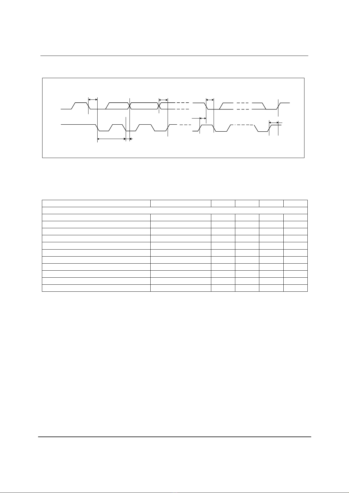
The audio data interface supports I2S, left justified, right
justified and DSP audio formats of 16-24 bit word length,
with sample rates from 32 to 192ks/s.
The device is supplied in a 20-lead Pb-free SSOP package.
FEATURES
•S/PDIF (IEC60958-3) compliant.
•Advanced jitter attenuating PLL with low intrinsic period
jitter of 50 ps RMS.
•S/PDIF recovered clock using PLL, or stand alone crystal
derived clock generation.
•Supports 10 – 27MHz crystal clock frequencies.
•2-wire / 3-Wire serial or hardware control interface.
•Programmable audio data interface modes:
- I2S, Left, Right Justified or DSP
- 16/20/24 bit word lengths
•1 channel receiver input and 1 channel transmit output.
•Auto frequency detection / synchronisation.
•Selectable output status data bits.
•Up to 3 configurable GPO pins.
•De-emphasis flag output.
•Non-audio detection including DOLBYTM and DTSTM.
•Channel status changed flag.
•Configurable clock distribution with selectable output
MCLK rate of 512fs, 256fs, 128fs and 64fs.
•2.7 to 3.6V digital and PLL supply voltages.
•20-lead SSOP package.
APPLICATIONS
•AV processors and Hi-Fi systems
•Music industry applications
•DVD-P/DVD-RW
•Digital TV
BLOCK DIAGRAM

WM8804 Production Data
w PD Rev 4.1 September 2007
2
TABLE OF CONTENTS
DESCRIPTION .......................................................................................................1
FEATURES.............................................................................................................1
APPLICATIONS .....................................................................................................1
BLOCK DIAGRAM .................................................................................................1
TABLE OF CONTENTS .........................................................................................2
PIN CONFIGURATION...........................................................................................3
ORDERING INFORMATION ..................................................................................3
PIN DESCRIPTION ................................................................................................4
ABSOLUTE MAXIMUM RATINGS.........................................................................5
RECOMMENDED OPERATING CONDITIONS .....................................................6
SUPPLY CURRENT ...................................................................................................... 6
ELECTRICAL CHARACTERISTICS ......................................................................6
MASTER CLOCK TIMING............................................................................................. 7
DIGITAL AUDIO INTERFACE – MASTER MODE......................................................... 7
DIGITAL AUDIO INTERFACE – SLAVE MODE ............................................................ 8
CONTROL INTERFACE – 3-WIRE MODE.................................................................... 9
CONTROL INTERFACE – 2-WIRE MODE.................................................................. 10
DEVICE DESCRIPTION.......................................................................................11
INTRODUCTION......................................................................................................... 11
POWER UP CONFIGURATION .................................................................................. 12
CONTROL INTERFACE OPERATION........................................................................ 14
HARDWARE CONTROL MODE.................................................................................. 18
DIGITAL ROUTING CONTROL................................................................................... 20
MASTER CLOCK AND PHASE LOCKED LOOP......................................................... 21
SOFTWARE MODE INTERNAL CLOCKING .............................................................. 21
HARDWARE MODE INTERNAL CLOCKING.............................................................. 30
S/PDIF TRANSMITTER............................................................................................... 31
S/PDIF RECEIVER...................................................................................................... 34
GENERAL PURPOSE OUTPUT (GPO) CONFIGURATION ....................................... 43
DIGITAL AUDIO INTERFACE ..................................................................................... 44
AUDIO DATA FORMATS ............................................................................................ 45
REGISTER MAP ......................................................................................................... 52
APPLICATIONS INFORMATION .........................................................................63
RECOMMENDED EXTERNAL COMPONENTS.......................................................... 63
PACKAGE DIMENSIONS ....................................................................................65
IMPORTANT NOTICE ..........................................................................................66
ADDRESS: .................................................................................................................. 66

Production Data WM8804
w PD Rev 4.1 September 2007
3
PIN CONFIGURATION
( Top View )
ORDERING INFORMATION
DEVICE TEMPERATURE
RANGE PACKAGE MOISTURE
SENSITIVITY LEVEL
PEAK SOLDERING
TEMPERATURE
WM8804GEDS -25 to +85oC 20-lead SSOP
(Pb-free) MSL1 260oC
WM8804GEDS/R -25 to +85oC 20-lead SSOP
(Pb-free, tape and reel) MSL1 260oC
Note:
Reel quantity = 2,000

WM8804 Production Data
w PD Rev 4.1 September 2007
4
PIN DESCRIPTION
PIN NAME TYPE DESCRIPTION
1 SCLK Digital In/Out Control interface clock / GPO in hardware control mode. See note 2.
2 GPO0 / SWIFMODE Digital In/Out General purpose digital output or selected functionality at hardware reset.
See note 2.
3 SDIN / HWMODE Digital Input Control interface data input and hardware/software mode select at hardware
reset. See note 2.
4 SDOUT / GPO2 Digital In/Out Control interface data output in 3-wire software control mode/ GPO in
hardware control mode or 2-wire software control mode. See note 2.
5 CSB / GPO1 Digital In/Out Chip select / GPO in hardware control mode or 2-wire software control
Mode. See note 2
6 RESETB Digital Input System reset (active low)
7 PVDD Supply PLL core supply
8 PGND Supply PLL ground
9 CLKOUT Digital Out High drive clock output at 64fs, 128fs, 256fs and 512fs
10 XOP Digital Output Crystal output
11 XIN Digital Input Crystal input
12 DOUT Digital Out Audio interface data output
13 DIN Digital In Audio interface data input
14 BCLK Digital In/Out Audio interface bit clock
15 LRCLK Digital In/Out Audio interface left/right word clock
16 MCLK Digital In/Out Master clock input or output
17 TX0 Digital Out S/PDIF transmit channel
18 DGND Supply Digital ground
19 DVDD Supply Digital core supply
20 RX0 Digital In S/PDIF receive channel
Notes:
1. Digital input pins have Schmitt trigger input buffers.
2. Refer to Table 6 Device Configuration at Power up or Hardware Reset

Production Data WM8804
w PD Rev 4.1 September 2007
5
ABSOLUTE MAXIMUM RATINGS
Absolute Maximum Ratings are stress ratings only. Permanent damage to the device may be caused by continuously operating at
or beyond these limits. Device functional operating limits and guaranteed performance specifications are given under Electrical
Characteristics at the test conditions specified.
ESD Sensitive Device. This device is manufactured on a CMOS process. It is therefore generically susceptible
to damage from excessive static voltages. Proper ESD precautions must be taken during handling and storage
of this device.
Wolfson tests its package types according to IPC/JEDEC J-STD-020B for Moisture Sensitivity to determine acceptable storage
conditions prior to surface mount assembly. These levels are:
MSL1 = unlimited floor life at <30°C / 85% Relative Humidity. Not normally stored in moisture barrier bag.
MSL2 = out of bag storage for 1 year at <30°C / 60% Relative Humidity. Supplied in moisture barrier bag.
MSL3 = out of bag storage for 168 hours at <30°C / 60% Relative Humidity. Supplied in moisture barrier bag.
The Moisture Sensitivity Level for each package type is specified in Ordering Information.
CONDITION MIN MAX
Digital core and I/O buffer supply voltage -0.3V +5V
PLL supply voltage -0.3V +5V
Voltage range digital inputs DGND -0.3V DVDD +0.3V
Master Clock Frequency 37MHz
Operating temperature range, TA-25°C +85°C
Storage temperature -65°C +150°C
Note:
1. PLL and digital supplies must always be within 0.3V of each other.
2. PLL and digital grounds must always be within 0.3V of each other.

WM8804 Production Data
w PD Rev 4.1 September 2007
6
RECOMMENDED OPERATING CONDITIONS
PARAMETER SYMBOL TEST CONDITIONS MIN TYP MAX UNIT
Digital supply range DVDD 2.7 3.6 V
Ground DGND 0 V
PLL supply range PVDD 2.7 3.6 V
Ground PGND 0 V
Notes:
1. PLL and digital supplies must always be within 0.3V of each other.
2. PLL and digital grounds must always be within 0.3V of each other.
SUPPLY CURRENT
PARAMETER SYMBOL TEST CONDITIONS MIN TYP MAX UNIT
Digital supply current IDVDD DVDD = 3.3V 14.9 mA
PLL supply current IPVDD PVDD = 3.3V 1.7 mA
Power Consumption DVDD/PVDD = 3.3V 54.8 mW
Standby Power
Consumption
DVDD/PVDD = 3.3V
Device powered down
0.11 mW
ELECTRICAL CHARACTERISTICS
Test Conditions
PVDD = 3.3V, DVDD = 3.3V, PGND = 0V, DGND = 0V, TA = +25oC, fs = 48kHz, MCLK = 256fs unless stated.
PARAMETER SYMBOL TEST CONDITIONS MIN TYP MAX UNIT
Jitter Characteristics
Intrinsic Period Jitter Ji50 ps
Digital Logic Levels (CMOS Levels)
Input LOW level VIL 0.3 x DVDD V
Input HIGH level VIH 0.7 x DVDD V
Output LOW VOL 0.1 x DVDD V
Output HIGH VOH 0.9 x DVDD V
Isource 25 mA
CLOCKOUT buffer drive
capability Isink
CMOS
20pF load 25 mA
S/PDIF Receiver Characteristics
Input Resistance 23 kΩ

Production Data WM8804
w PD Rev 4.1 September 2007
7
MASTER CLOCK TIMING
MCLK
t
MCLKL
t
MCLKH
t
MCLKY
Figure 1 Slave Mode MCLK Timing Requirements
Test Conditions
PVDD = 3.3V, DVDD = 3.3V, PGND = 0V, DGND = 0V, TA = +25oC, fs = 48kHz, MCLK = 256fs unless stated.
PARAMETER SYMBOL TEST CONDITIONS MIN TYP MAX UNIT
System Clock Timing Information – Slave Mode
MCLK System clock cycle time tMCLKY 27 ns
MCLK System clock pulse width high tMCLKH 11 ns
MCLK System clock pulse width low tMLCKL 11 ns
MCLK Duty cycle 40:60 60:40 %
Table 1 Master Clock Timing Requirements
DIGITAL AUDIO INTERFACE – MASTER MODE
BCLK
DOUT
LRCLK
t
DL
DIN
t
DDA
t
DHT
t
DST
Figure 2 Digital Audio Data Timing – Master Mode
Test Conditions
PVDD = 3.3V, DVDD = 3.3V, PGND = 0V, DGND = 0V, TA = +25oC, fs = 48kHz, MCLK = 256fs unless stated.
PARAMETER SYMBOL TEST CONDITIONS MIN TYP MAX UNIT
Audio Data Input Timing Information
LRCLK propagation delay from
BCLK falling edge
tDL 0 10 ns
DOUT propagation delay from
BCLK falling edge
tDDA 0 10 ns
DIN setup time to BCLK rising
edge
tDST 10 ns
DIN hold time from BCLK rising
edge
tDHT 10 ns
Table 2 Digital Audio Data Timing – Master Mode

WM8804 Production Data
w PD Rev 4.1 September 2007
8
DIGITAL AUDIO INTERFACE – SLAVE MODE
BCLK
LRCLK
t
BCH
t
BCL
t
BCY
DIN
DOUT
t
LRSU
t
DS
t
LRH
t
DH
t
DD
Figure 3 Digital Audio Data Timing – Slave Mode
Test Conditions
PVDD = 3.3V, DVDD = 3.3V, PGND = 0V, DGND = 0V, TA = +25oC, fs = 48kHz, MCLK = 256fs unless stated.
PARAMETER SYMBOL TEST CONDITIONS MIN TYP MAX UNIT
Audio Data Input Timing Information
BCLK cycle time tBCY 50 ns
BCLK pulse width high tBCH 20 ns
BCLK pulse width low tBCL 20 ns
LRCLK set-up time to BCLK
rising edge
tLRSU 10 ns
LRCLK hold time from
BCLK rising edge
tLRH 10 ns
DIN set-up time to BCLK
rising edge
tDS 10 ns
DIN hold time from BCLK
rising edge
tDH 10 ns
DOUT propagation delay
from BCLK falling edge
tDD 0 10 ns
Table 3 Digital Audio Data Timing – Slave Mode

Production Data WM8804
w PD Rev 4.1 September 2007
9
CONTROL INTERFACE – 3-WIRE MODE
Figure 4 Control Interface Timing – 3-Wire Serial Control Mode
Test Conditions
PVDD = 3.3V, DVDD = 3.3V, PGND = 0V, DGND = 0V, TA = +25oC, fs = 48kHz, MCLK = 256fs unless stated.
PARAMETER SYMBOL MIN TYP MAX UNIT
Program Register Input Information
SCLK rising edge to CSB rising edge tSCS 60 ns
SCLK cycle time tSCY 80 ns
SCLK duty cycle 40/60 60/40 %
SDIN to SCLK set-up time tDSU 20 ns
SDIN hold time from SCLK rising edge tDHO 20 ns
SDOUT propagation delay from SCLK rising edge tDL 5 ns
CSB pulse width high tCSH 20 ns
CSB rising/falling to SCLK rising tCSS 20 ns
SCLK glitch suppression tps 2 8 ns
Table 4 Control Interface Timing – 3-Wire Serial Control Mode

WM8804 Production Data
w PD Rev 4.1 September 2007
10
CONTROL INTERFACE – 2-WIRE MODE
SDIN
SCLK
t
STHO
t
SCY
t
DSU
t
STSU
t
STHO
t
STOP
t
DH
Figure 5 Control Interface Timing – 2-Wire Serial Control Mode
Test Conditions
PVDD = 3.3V, DVDD = 3.3V, PGND = 0V, DGND = 0V, TA = +25oC, fs = 48kHz, MCLK = 256fs unless stated.
PARAMETER SYMBOL MIN TYP MAX UNIT
Program Register Input Information
SCLK cycle time tSCY 2500 ns
SCLK duty cycle 40/60 60/40 %
SCLK frequency 400 kHz
Hold Time (Start Condition) tSTHO 600 ns
Setup Time (Start Condition) tSTSU 600 ns
Data Setup Time tDSU 100 ns
SDIN, SCLK Rise Time 300 ns
SDIN, SCLK Fall Time 300 ns
Setup Time (Stop Condition) tSTOP 600 ns
Data Hold Time tDH 900 ns
SCLK glitch suppression tps 2 8 ns
Table 5 Control Interface Timing – 2-Wire Serial Control Mode

Production Data WM8804
w PD Rev 4.1 September 2007
11
DEVICE DESCRIPTION
INTRODUCTION
FEATURES
•IEC-60958-3 compatible with 32 to 192k frames/s support.
•Supports AES-3 data frames.
•Support for reception and transmission of S/PDIF data.
•Clock synthesis PLL with reference clock input and low jitter output.
•Supports input reference clock frequencies from 10MHz to 27MHz.
•Dedicated high drive clock output pin.
•Register controlled channel status bit configuration.
•Register read-back of recovered channel status bits and error flags.
•Detection of non-audio data, sample rate and de-emphasis.
•Programmable GPOs for error flags and frame status flags.
The WM8804 is an IEC-60958 compatible S/PDIF transceiver with support for one received S/PDIF
data stream and one transmitted S/PDIF data stream.
The receiver performs data and clock recovery, and transmits recovered data from the chip either
through the digital audio interface or, alternatively, the device can loop the received S/PDIF data
back out through the S/PDIF transmitter producing a de-jittered S/PDIF transmit data stream. The
recovered clock may be routed to a high drive output pin for external use. If there is no S/PDIF input
data stream the PLL can be configured to output all standard MCLK frequencies or it can be
configured to maintain the frequency of the last received S/PDIF data stream.
The transmitter generates S/PDIF frames where audio data may be sourced from the S/PDIF
receiver or the digital audio interface. Timing for the S/PDIF transmitter interface can be sourced
from the internally derived MCLK in loop through mode or it can be taken from an external source.
S/PDIF FORMAT
S/PDIF is a serial, bi-phase-mark encoded data stream. An S/PDIF frame consists of two sub-
frames. Each sub-frame is made up of:
•Preamble – a synchronization pattern used to identify the start of a 192-frame block or sub-
frame
•4-bit Auxiliary Data (AUX) – ordered LSB to MSB
•20-bit Audio Data (24-bit when combined with AUX) – ordered LSB to MSB
•Validity Bit – a 1 indicates invalid data in the associated sub-frame
•User Bit – over 192-frames, this forms a User Data Block
•Channel Bit – over 192-frames, this forms a Channel Status Block
•Parity Bit – used to maintain even parity over the sub-frame (not including the preamble)
An S/PDIF Block consists of 192 frames. Channel and user blocks are incorporated within the 192-
frame S/PDIF Block. For Consumer mode only the first 40-frames are used to make up the Channel
and User blocks. Figure 6 illustrates the S/PDIF format. The WM8804 does not support transmission
of user channel data. Received user channel data may be accessed via GPO pins.

WM8804 Production Data
w PD Rev 4.1 September 2007
12
. . . . . . . . .
Frame
192
Frame
1
Subframe 1 Subframe 2
Sync
preamble Aux V U C PAudio Sample Word
3 4 7 8 27 28031
32 bits
Figure 6 S/PDIF Format
POWER UP CONFIGURATION
The operating mode of the WM8804 is dependent upon the state of SDIN, SCLK, SDOUT, CSB and
GPO0 when the device is powered up or a hardware reset occurs. Table 6 summarises the
configuration options.
HW RESET = 0 HW RESET = 1
SWMODE HWMODE SWMODE HWMODE
SDIN HWMODE / SWMODE Select SDIN N/A
SCLK N/A AIF_MS SCLK GPO
(TRANS_ERR)
2-wire 3-wire
SDOUT N/A AIF_CONF[0]
GPO SDOUT
GPO
(NON_AUDIO)
2-wire 3-wire 2-wire 3-wire
CSB Device
Address N/A
TXSRC
GPO CSB
GPO
(UNLOCK)
PIN
GPO0
2-wire/3-wire
Mode Select
AIF_CONF[1] GPO
GPO
(GEN_FLAG)
Note: AIF_CONF[1:0] configures the audio interface when the device operates in hardware mode.
Refer to Table 16 for description of modes.
Table 6 Device Configuration at Power up or Hardware Reset

Production Data WM8804
w PD Rev 4.1 September 2007
13
When the device powers up, all power up configuration pins are configured as inputs for a minimum
of 9.4us and a maximum of 25.6us following the release of the external reset. The times are based
on 27MHz and 10MHz crystal clock frequencies respectively. This enables the pins to be sampled
and the device to be configured before the pins are released to their selected operating conditions.
Figure 7 illustrates how SDIN is sampled.
Figure 7 Pin Sampling On Power Up or Hardware Reset
If the device is powered up in software control mode, all functions of the device are powered down by
default and must be powered up individually by writing to the relevant bits of the PWRDN register
(Table 7). In hardware control mode, all functions of the device are powered up by default.
REGISTER ADDRESS BIT LABEL DEFAULT DESCRIPTION
0 PLLPD 1 PLL powerdown
0 = PLL enabled
1 = PLL disabled
1 SPDIFRXP
D
1 S/PDIF receiver powerdown
0 = S/PDIF receiver enabled
1 = S/PDIF receiver disabled
2 SPDIFTXPD 1 S/PDIF transmitter powerdown
0 = S/PDIF transmitter enabled
1 = S/PDIF transmitter disabled
3 OSCPD 0 Oscillator power down
0 = Power Up
1 = Power Down
4 AIFPD 0 Digital audio interface power
down
0 = Power Up
1= Power Down
R30
PWRDN
1Eh
5 TRIOP 0 Tri-state all outputs
0 = Outputs not tri-stated
1 = Outputs tri-stated
Table 7 Power Down Register
D Q
ENB
SDIN
RSTB
Powe
r
-
On Reset
POR_B
HWMODE
/
SWMODE
Sampling of pin value at reset to
generate internal signals.

WM8804 Production Data
w PD Rev 4.1 September 2007
14
CONTROL INTERFACE OPERATION
Control of the WM8804 is implemented in either hardware control mode or software control mode.
The method of control is determined by sampling the state of the SDIN/HWMODE pin at power up or
at a hardware reset. If SDIN/HWMODE is low during power up the device is configured in hardware
control mode, otherwise the device is configured in software control mode.
SDIN/HWMODE
0 Hardware mode
1 Software mode
Table 8 Hardware or Software Mode Select
Software control is achieved using a 3-wire (3-wire write, 4-wire read) or a 2-wire serial interface.
The serial interface format is configured by sampling the state of the GPO0/SWIFMODE pin on
power up or at a hardware reset. If the GPO0/SWIFMODE pin is low the interface is configured in 2-
wire mode, otherwise the interface is configured in 3-wire SPI compatible mode.
GPO0/SWIFMODE
0 2-wire interface
1 3-wire interface
Table 9 Software Mode Control Interface Select
3-WIRE (SPI COMPATIBLE) SERIAL CONTROL MODE – REGISTER WRITE
SDIN is used for the program data, SCLK is used to clock in the program data and CSB is used to
latch in the program data. SDIN is sampled on the rising edge of SCLK. The 3-wire interface write
protocol is shown in Figure 8.
Figure 8 3-Wire Serial Interface Register Write Protocol
•W is a control bit indicating a read or write operation. 0 =write operation, 1 = read operation
•REGA[6:0] is the register address.
•DIN[7:0] is the data to be written to the register being addressed.
•CSB is edge sensitive – the data is latched on the rising edge of CSB.

Production Data WM8804
w PD Rev 4.1 September 2007
15
3-WIRE SERIAL CONTROL MODE REGISTER READ-BACK
Not all registers can be read. Only the device ID (registers R0, R1 and R2) and the status registers
can be read. These status registers are labelled as “read only” in the Register Map section.
The read-only status registers can be read back via the SDOUT pin. The registers can be read by
one of two methods, selected by the CONT register bit and the ‘W’ control bit. The oscillator must be
powered up before 3-wire control interface read-back is possible.
When CONT =1 and ‘W’=0, a single read-only register can be read back by writing to any other
register or to a dummy register. The register to be read is determined by the READMUX[2:0] bits.
When a write to the device is performed, the device will respond by returning the status byte in the
register selected by the READMUX register bits. This 3-wire interface read back method using a write
access is shown in Figure 9.
REGISTER ADDRESS BIT LABEL DEFAULT DESCRIPTION
2:0 READMUX
[2:0]
000 Status Register Select
Determines which status register
is to be read back:
000 = Interrupt Status Register
001 = Channel Status Register 1
010 = Channel Status Register 2
011 = Channel Status Register 3
100 = Channel Status Register 4
101 = Channel Status Register 5
110 = S/PDIF Status Register
R29
SPDRX1
1Dh
3 CONT 0 Continuous Read Enable
0 = Continuous read-back mode
disabled
1 = Continuous read-back mode
enabled
Table 10 Read-Back Control Register
The SDOUT pin is tri-state unless CSB is held low; therefore CSB must be held low for the duration
of the read.
Figure 9 3-Wire Control Interface Read-Back Method 1
The second method of reading the read only status registers is If CONT=0 and ‘W’=1. Using this
method the user can read back directly from a register by reading the register address. The device
will respond with the contents of the register. The protocol for this read-back method is shown in
Figure 10.

WM8804 Production Data
w PD Rev 4.1 September 2007
16
Figure 10 3-Wire Control Interface Read-Back Method 2
2-WIRE SERIAL CONTROL MODE - REGISTER WRITE
The WM8804 supports software control via a 2-wire serial bus. Many devices can be controlled by
the same bus and each device has a unique 7-bit address (see Table 11).
The controller indicates the start of data transfer with a high to low transition on SDIN while SCLK
remains high. This indicates that a device address, DEVA(7:1), and data, REG(6:0), will follow. All
devices on the 2-wire bus will shift in the next eight bits on SDIN (7-bit address DEVA(7:1), +
read/write ‘W’ bit, MSB first). If the device address received matches the address of the WM8804,
the WM8804 responds by driving SDIN low on the next clock pulse (ACK). This is a device
acknowledgement of an address match. If the address does not match that of the WM8804, the
device returns to the idle condition and waits for a new start condition and valid address.
Once the WM8804 has acknowledged a matching address, the controller sends the first byte of
control data, which is the WM8804 register address (REGA[6:0]). The WM8804 then acknowledges
reception of the control data byte by pulling SDIN low for one clock pulse (another ACK). The
controller then sends the second byte of control data (DIN[7:0], i.e. the eight bits of register data to
be written), and the WM8804 acknowledges again by pulling SDIN low (another ACK).
The transfer of data is complete when there is a low to high transition on SDIN while SCLK is high.
After receiving a complete address and data sequence the WM8804 returns to the idle state and
waits for another start condition. If a start or stop condition is detected out of sequence at any point
during data transfer (i.e. SDIN changes while SCLK is high), the device returns to the idle condition.
Figure 11 2-Wire Serial Control Interface Write

Production Data WM8804
w PD Rev 4.1 September 2007
17
Multiple consecutive register writes can be performed in 2-wire control mode by setting the CONT bit
high. This method allows the entire register map to be defined in a one continuous write operation.
Figure 12 2-Wire Serial Control Interface Multi-Write
The WM8804 has two possible device addresses, which can be selected using the CSB pin during
hardware reset.
CSB STATE DEVICE ADDRESS IN
2-WIRE MODE
ADDRESS (X=R/W BIT)
X=0 X= 1
Low 0111010x 0x7A 0x75
High 0111011x 0x76 0x77
Table 11 2-Wire Interface Address Selection
2-WIRE SERIAL CONTROL MODE -REGISTER READ-BACK
The WM8804 allows read-back of certain registers in 2-wire mode. The protocol is similar to that
used to write to the device. The controller will issue the device address followed by a write bit, the
register index will then be passed to the WM8804. At this point the controller will issue a repeated
start condition and resend the device address along with a read bit. The WM8804 will acknowledge
this and the WM8804 will become a slave transmitter. The WM8804 will transmit the data from the
indexed register on SDIN MSB first. When the controller receives the data it will not acknowledge
receipt of the data indicating that it will resume master transmitter control of SDIN. The controller will
then issue a stop command completing the read cycle. Figure 13 illustrates the read protocol.
Figure 13 2-Wire Serial Control Interface Read (CONT=0)
2-WIRE SERIAL CONTROL MODE – CONTINUOUS READ-BACK
As in 3-wire mode, there are two methods of reading back data: continuous and non-continuous
read-back. Continuous read-back is selected by setting CONT to 1. In continuous read-back mode,
the device will return the indexed register first followed by consecutive registers in increasing index
order until the controller does not acknowledge the data then issues a stop sequence. This is shown
in Figure 14
Figure 14 2-Wire Serial Interface Continuous Read-Back (CONT=1)

WM8804 Production Data
w PD Rev 4.1 September 2007
18
SOFTWARE REGISTER RESET
Writing to register 0000000 will reset the WM8804. This will reset all register bits to their default
values. The WM8804 is powered down by default so writing to this register will power down the
device.
DEVICE ID AND REVISION IDENTIFICATION
Registers 0,1 and 2 can be read to identify the device ID and IC revision number. Refer to Table 12
for details.
REGISTER
ADDRESS
BIT LABEL DEFAULT DESCRIPTION
RESET N/A
Writing to this register will apply a
reset to the device.
R00
RST/DEVID1
00h
7:0
DEVID1[7:0] 00000101
Reading from this register will return
the second part of the device ID
00000101 = 0x05
R01
DEVID2
01h
(read only)
7:0 DEVID2[7:0] 10001000
Reading from this register will return
the first part of the device ID
10001000 = 0x88
R02
DEVREV
02h
3:0 DEVREV
[3:0] N/A
Reading from this register will return
the device revision.
0x1 = revision 1
Table 12 Software Reset Register and Device ID
HARDWARE CONTROL MODE
The WM8804 can be operated in either software or hardware control modes. The method of control
is determined by sampling the state of the SDIN pin during power up or hard reset. If SDIN is LOW
during power up or hardware reset, the WM8804 will be switched into hardware control mode.
PIN 0 1
SDIN Hardware control Mode Software control Mode
Table 13 Hardware / Software Mode Configuration
In hardware control mode the user has limited control over the configuration of the device. Most of
the features will assume default values but some can be configured using external pins. When the
device is configured in hardware control mode, all functions of the device are powered up.
The clock and data recovery module requires a 12 MHz crystal derived clock reference as the
default values for this module cannot be altered in hardware control mode.
MASTER / SLAVE MODE SELECTION
The WM8804 can be configured in either master or slave mode. In software control mode this is set
by writing to AIF_MS in the AIFRX register. In hardware control mode this is controlled by sampling
the SCLK pin on power up or hardware reset.
PIN
(HARDWARE
MODE)
REGISTER
(SOFTWARE
MODE)
0 1
SCLK AIF_MS Slave mode Master mode
Table 14 Master / Slave Mode Configuration in Hardware Mode

Production Data WM8804
w PD Rev 4.1 September 2007
19
DIGITAL ROUTING CONTROL
See page 20 for a full description of the signal routing options available in the WM8804. In Software
control mode the value set in register TXSRC determines the S/PDIF transmitter data source. In
hardware control mode the value of TXSRC can be set using the CSB pin.
PIN
(HARDWARE
MODE)
REGISTER
(SOFTWARE
MODE)
0 1
CSB TXSRC S/PDIF Rx AIF Rx
Table 15 S/PDIF Transmitter Digital Routing Control Configuration
AUDIO INTERFACE CONTROL
In software control mode the audio data word length and audio data format can be set independently
for the receiver and transmitter sides of the interface. However, in hardware control mode both sides
of the interface are combined and the configuration is set using SDOUT and GPO0 pins as described
in Table 6 and Table 16. Note that AIF_CONF[1:0] configures the audio interface when the device
operates in hardware mode.
GPO0 /
AIFCONF[1]
SDOUT /
AIFCONF[0]
DESCRIPTION
0 0 16-bit I2S
0 1 24-bit I2S
1 0 24-bit Left Justified With Flags
1 1 16-bit Right Justified
Table 16 Digital Audio Interface Control in Hardware Control Mode
STATUS INFORMATION
In hardware control mode the WM8804 outputs a selection of status flags for the user. Table 17
describes the flags which are available and the output pins on which they are available.
PIN STATUS FLAG
SCLK TRANS_ERR
SDOUT NON_AUDIO
CSB UNLOCK
GPO0 GEN_FLAG
Table 17 Hardware Control Mode Status Flag Configuration
A full description of the status flags is given in Table 45.

WM8804 Production Data
w PD Rev 4.1 September 2007
20
DIGITAL ROUTING CONTROL
Figure 15 Digital Routing Paths within the WM8804
Digital signal routing within the WM8804 is controlled by the TXSRC register. In order to ensure
proper operation when changing TXSRC, the S/PDIF transmitter module should be powered down
prior to changing the TXSRC control register and powered up again once the routing path has been
changed.
REGISTER
ADDRESS
BIT LABEL DEFAULT DESCRIPTION
R30
PWRDN
1Eh
2 SPDIFTXPD 1 S/PDIF Transmitter Powerdown
0 = S/PDIF transmitter enabled
1 = S/PDIF transmitter disabled
R21
SPDTX4
15h
6 TXSRC 1 S/PDIF Transmitter Data Source
0 = S/PDIF Received Data –
SPDIFTXCLK Source = CLK2
1 = Digital Audio Interface
Received Data – SPDIFTXCLK
Source = MCLK Input/Output
Signal at MCLK Pin
Table 18 Digital Signal Routing Control Registers
Table of contents
Other Wolfson Transceiver manuals