KCU1250 User Guide www.xilinx.com 8
UG1057 (v1.0) December 19, 2014
Chapter 1: KCU1250 Board Features and Operation
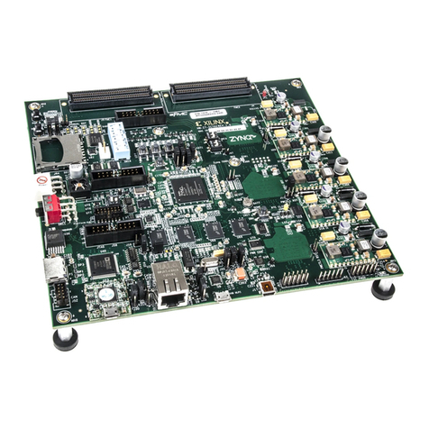
Tab le 1- 1 describes the callouts in Figure 1-2.
Table 1-1: KCU1250 Board Features and Operation
Figure
1-2
Callout
Reference Designator Feature Description
1 U1 UltraScale XCKU040-2FFVA1156E FPGA, page 18
2 SW1 Power switch, page 10
3 J28 12V mini-fit connector, page 9
4J37, J38, J39, J40, J41, J42, J43 GTH transceiver connector pads Q224, Q225, Q226, Q227, Q228
page 28
5 U80 Digilent USB JTAG connector (micro-B receptacle), page 18
6J2 Platform USB JTAG connector (alternate access for programming
cables), page 18
7 J10 SD card connector (back-side of board), page 18
8 SW13 System controller configuration DIP switches, page 21
9 SW4 System controller power on reset (SYS_POR) button, page 20
10 J36 SuperClock-2 module, page 24
11 U42 300 MHz LVDS oscillator, page 23
12 DS17 FPGA DONE status LED, page 25
13 DS3 FPGA INIT status LED, page 25
14 SW7 FPGA PROGRAM pushbutton, page 27
15 DS18 12V system power status LED, page 14
16 DS4, DS5, DS6, DS7, DS8, DS9,
DS10, DS28, DS13, DS14, DS15
Status LEDS for FPGA logic, transceiver and utility power
17 SW2 Power regulation inhibitor switch for onboard regulators, page 13
18 J5, J25, J26, J27 External power supply connectors, page 13 and page 14
19 J46, J124 MGT transceiver power supply module, page 15
20 J21 FPGA and utility rails PMBUS connector, page 14
21 J4 MGT rails PMBUS connector, page 13
22 J1 Connector for USB to dual-UART bridge (mini-B receptacle), page 23
23 J99 Power connector for active heatsink, page 16
24 DS19, DS20, DS21, DS22, DS23,
DS24, DS25, DS26
User LEDs (active-High), page 25
25 SW8, SW9 User pushbuttons (active-High), page 27
26 SW3 User DIP switches (active-High), page 26
27 J95 User I/O header, page 27
28 JA2 FMC1 connector, page 35
29 JA3 FMC2 connector page 38
