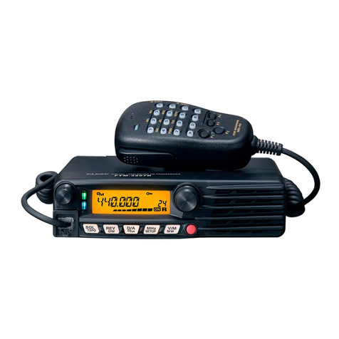
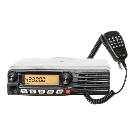
Yaesu FT-2500M Manual

FTIZ^SOOM
Mil-Spec 2-m FM Tkansceiver
Technical Supplement
YAESU MUSEN CO., LTD.
C.P.O. Box 1500, Tokyo, Japan
YAESU U.S.A.
17210 Edwards Rd., Cerritos, California 90203
U.S.A.
YAESU EUROPE B.V.
Snipweg 3. U18DN Schiphol, The Netherlands
YAESU UK LTD.
Unit 2, Maple Grove Business Centre
Lawrence Rd., Hounslow, Middlesex TW4 6DR, UK
n

Contents
I. General Information
Introduction . .1,-l
Specifications . . . . .].-2
ChipComponentlnformation ....L-3
CircuitDescription . , . .'1,-7
Block Diagram .1_-11
InterconnectionDiagram ...1-13
ExplodedView&MiscellaneousParts ...L-15
II. Servicing
Case Disassembly & PCB Access
LCD & Control Unit Access
Lithium Backup Battery Replacement
Panel Lamp Replacement
9600 Baud Packet Modification
Channel Display-Only Mode
. . .2-'1,
2-l
2-'t
2-1.
,-1
2-4
Alignment.. .....2-5
PLL & Transmitter 2-6
PLL VCV (Varactor Control Voltage) . . . 2-6
PLLReferenceFrequency . . . . .2-7
TrqnsmitterOutput ..2-7
TiansmitterDeai.ation . . . . . .2-7
Receiver 2-g
InterstageTransformers ......2-8
S-MeterCalibration . .2-B
ScannerCenterStop. ......2-B
Squelch ....2-B
III. Board Units (Schematics, Layout & Parts List)
VCOUnit. ...3A-L
MAINUnit. . .38-L
MIC Unit
CNTLUnit . ..3D-L
DISPLAYUnit. ....3E-1,
IV. Optional Board Units (Schematics, Layout & Parts)
FRC-5 DTMF Paging Unit . . 4A-'t_
FTS-L7A CTCSS Tone Squelch Unit . . . .48-1-
MH-26csyMicrophone . . . .4C
llv{IJ-z7 AsI Microphone . . 4D-7
Cut out the label at the right and place
it behind the clear plastic window in
the spine of the manual binder.
FT-2500M
Technical Supplement

V' Introduction
The FT-2500M is Yaesu's new successor to the
famous FT-2400H, the industry's first amateur
transceiver designed to meet rugged U'S' mili-
tary specifications for shock and vibration (MIL-
SPEC 810-C). The FT-2500M is upgraded with a
new front panel and control knob layout, and
additional operator features.
Selectable power output of 5,25 or 50 watts
without the need of forced air cooling is possible
due to the large heatsink surface area of the com-
partmentalized one-piece diecast chassis. Back-
lighting for the large LCD (display) and knobs is
m-anually adjustable, or automatically controlled
by a photosensor, and the less-used buttons have
a flip-down protective cover. The thirty-one tun-
able memories can each be programmed with a
4-character channel name, which can thenbe dis-
played in place of frequency, as desired.
Each memory offers complete programmabil-
ity and scanning functions, such as independent
tx/ rx frequencies, independent repeater offset
and CTCSS tone, prografiunable scan limits, se-
lectable scan resume modes and memorY skiP,
priority monitoring and a l-touch instant-recall
CALL channel. Channel steps are user-selectable
from 5 to 50 kHz, and Automatic Repeater Shift
can set standard repeater shifts when you tune to
a repeater subband. A1750-Hz tone generator is
included in European versions. A 39-tone Pro-
grammable CTCSS encoder is built in as stand-
ard, and the FTS-17ACTCSS unit canbe installed
to provide tone squelched private channels and a
CTCSS paging bell feature to sound a paging
alert tone when the tone squelch opens.
DTMF (Dual-Tone, Multi-Frequency) -based
selective calling and private paging capabilities
can be easily added with the optional FRC-6,
controlled entirely from the front panel. You can
select any of 999 3-digit ID codes for your trans-
ceiver, and then have your receiver stay quiet
until your code is received (frorn any standard
DTMF-equipped transceiver). When a call is re-
ceived, the FT-2500M displays the caller's code,
and a pagingbeeper canbe set to sound and even
to respond to the call automatically. Seven DTMF
code memories store your ID plus those of six
other frequently-called stations or grouPs you
wish to monitor.
FT-2500M Technical Supplement 1-1

Specifications
General
Frequency Range: t44-146 or 148 MHz T>; or 144-146 MHz or 1.40-174MHz Rx ,_____,
Channel Steps: 5,10,L2.5,I5,20,25 & 50 kHz
Frequency Stability: < +10 ppm (-20" to +60'C)
Mode of Emission: G3E (F3)
Antenna Impedance: 50 ohms, unbalanced
Supply voltage: 13.8 VDC +10"/", negative ground
Current Consumption (typical): Rx: 600 mA, Tx hr/mid/low:12/9/5A
Operating T"*p. Range: -20o to +60" C
Case Size (WHD): 160 x 50 x 180 mm (w/o knobs)
Weight: 1.5 kg (3.31b.)
Transmitter \-/
OutputPower (high/mid /\ow): 50/25/5W
Modulation Type: Variable Reactance
MaximumDeviation: t5 kHz
Spurious Radiation: less than -60 dB
Microphone Impedance: 2kQ
\v
Receiver
Circuit Type: Double Conversion Superheterodyne
IFs: 21.4}l4'}lz & 455 kHz
Sensitivity (for 12dB SINAD): better than 0.2 pV
Selectivity (-6/-60 dB): 12/30kHz
IF Rejection: better than 70 dB
Image Rejection: better than 70 dB
Maximum AF Output: 3.5 W into 4 ohms @10% THD
Specifications are subject to change without notice or obligation.
FT-2500M Technical Supplement
t-
1-2

r
The diagrams below indicate some of the
distinguishing features of common chip com-
ponents.
Capacitors
l\
>.1 \
Tantalum Capacitors
Resistors
p Component Information
Type RMC 1/10W 1/16W
Marking* I00,222,47 3"" "
ll
t--l
Ten unit One
-@
Q
INDICATED
12
55
t0
LETTERS
tl
!a
TO
oExamples i
100 : 10O
222 : 2.2kO
473 :47kQ
(Unit I mm)
Type LwT
3216
2125
r 608
3.2
2.0
t.6
t.6
1.25
0.8
0.45-0.60
0.35-0.50
0.65-0.95
Type LwT
t /t0
1 /16
2.0
t.6
1.25
0.8
0 .45
0.45 00r0"
I1l0'
22td
33td
44t0
5510'
66td
7710'
BBtCI
IItd
FT-2500M Technical Supplement 1-3

\-------_
Chip Component Information
Replacing Chip Comp onents
Chip components are installed at the factory
by a series of robots. The first one places a spot
of adhesive resin at the location where each
part is to be installed, and later robots handle
and place parts using vacutun suction.
For single-sided boards, solder paste is ap-
plied and the board is then baked to harden the
resin and flow the solder. For double-sided
boards, no solder paste is applied, but the
board is baked (or exposed to ultra-violet light)
to cure the resin before dip soldering.
In our laboratories and service shops, small
quantities of chip components are mounted
manually by applying a spot of resin, placing
them with tweezers, and then soldering by
very small dual streams of hot air (without
physical contact during soldering). We remove
parts by first removing solder using a vacuurn
suction iron, which applies a light, steady vac-
uum at the iron tip, and then breaking the
adhesive with tweezers.
The special vacuum soldering/desoldering
equipment is recommended if you expect to do
a lot of chip replacements. Otherwise, it is
usually possible to remove and replace chip
components with only a tapered, temperature-
controlled soldering iron, a set of tweezers and
braided copper solder wick. Soldering iron
temperature should be less than 280'C (536
"F).
Precautions for Chip Replacement
X Do not disconnect a chip forcefully, or the
foil pattern may peel off the board.
X Never re-use a chip component. Dispose of
all removed chip components immediately
to avoid mixing with new parts.
X Limit soldering time to 3 seconds or less to
avoid damaging the component and board.
Remouing Chrp Comp onents
3 Remove the solder at each joint, one joint at
a time, using solder wick whetted with
non-acidic flux as shown below. Avoid ap-
plying pressure, and do not attempt to re-
move the tinning from the chip's electrode.
Grasp the chip on both sides with tweezers,
and gently twist the tweezers back and
forth (to break the adhesive bond) while
alternately heating each electrode. Be care-
ful to avoid peeling the foil traces from the
board. Dispose of the chip when removed.
D After removing the chip, use the copper
braid and soldering iron to which away any
excess solder and smooth the land for in-
stallation of the replacement part.
tr
1-4 FT-2500M Technical Supplement

Chip Component Information
Install a Replacement Chip
As thevalue of some chip components is not
\__ indicated on the body of the chip, be careful to
get the right part for replacement.
D Apply a small amount of solder to the land
on one side where the chip is to be installed.
Avoid too much solder, which may cause
bridging (shorting to other parts).
\=\
fl Hold the chip with tweezers in the desired
position, and apply the soldering iron with
a motion line that indicated by the arrow in
the diagram below. Do not apply heat for
more than 3 seconds.
tl Remove the tweezers and
trode on the other side in
described.
solder the elec-
the manner just
FT-2500M Technical Supplement 1-5

Notes
1-6 FT-2500M Technical Supplement

Circuit Descripton
Receioe Signal Path
Incoming RF from the antenna jack is deliv-
ered to the Main Unit and passed through a low-
pass filter and a I/+-wave antenna switching
network consisting of coils L1003 & Ll-004, ca-
pacitors C1003 & C1004, and diodes D1001 &
D1025. Signals within the frequency range of the
transceiver are then passed through a varactor-
tuned bandpass filter consisting of T1001/T1002
before RF amplification by Q1001 (3SK131). The
amplified RF is then bandpass filtered again by
varactor-tuned resonators T1,003/T1004, to en-
sure pure in-band input to 1st mixer
Q1002/Q1003 (2SK302GR x 2).
Buffered output from the VCO Unit is ampli-
fied by Q1005 (25C2759) and lowpass filtered by
LL009 and C1.042/C1043, to provide a pure 1st
local signal between LL8.6 and 152.6MH.2 to the
1st mixer. The 21.4-MHz 'l.st mixer product is
passed through dual monolithic crystal filter
XF1001 & XF1002 (t7.5 kHz BW) to strip away all
but the desired signal, which is then amplified by
Q1004 (25C2714Y).
The amplified 1st IF signal is applied to FM IF
subsystem IC Q1008 (MC3372ML), which con-
tains the 2nd mixer, 2nd local oscillator, limiter
amplifier, noise amplifie1, S-meter amplifier and
squelch gates. A 2nd local signal is generated
from 21.855 MHz crystal XL001, which produces
the 455 kHz 2nd IF when mixed with the 1st IF
signal within Q1008. The 2nd IF is passed
through ceramic filter CF1001 to strip away un-
wanted mixer products, and then applied to the
limiter amp in Q1008, which removes amplitude
variations in the 455 kHz IF before detection of
the speechby ceramic discriminator CD1001.
Detected audio is delivered from Q1008 to the
CNTL Unit, where it passes through buffer am-
plifier Q2018 (2sc2712cR) and audio gateQ2002
(DTC114EK) before de-emphasis, and high-pass
filtering by Q2001-2 (NJM29O2Mj/4). Another
audio muting gate, Q2003 (DTC114EK), passes
the signal, which is then combined with beeper
audio originating from the microprocessor
through Beeper volume trimrner VR2001. The
level of the combined receiver and beeper audio
on the CNTL Unit is set by VOL potentiometer
VR3002 on the DISP Unit and is then retumed the
Main Unit for amplification by Q1023
(TDA2003H) up to 2 watts for the optional head-
phone jack or 8-ohm loudspeaker.
Squelch Control
The squelch circuit consists of noise amplifier
Q1007 (2S'C2712GR) and a highpass filter and
squelch trigger within Q1008 on the MAIN Unit,
and control circuitry within microprocessor
Q2006 (SC418082CFU) on the CNTL Unit.
When no carrier is received, noise at the out-
put of the detector stage in Q1008 is amplifiedby
Q1007 and highpass filtered by the noise amp
section of Q1008, and then rectified by D1012 to
provide a DC control voltage for the squelch
switching section within Q1008. With no carrier,
pin 14 of Q1008 is high. This signal is inverted by
Q1006 (lMHs) and delivered to BUSY pin 15 of
main microprocessor Q2006 on the CNTLUnit as
the Scan Stop signal, which causes the BUSY indi-
cation on the display when the squelch is open.
This signal also causes the microprocessor to cut
receiver audio in two places on the CNTL Unit
mentioned already: opening audio mute gate
Q2002, and pulling the audio line to ground just
before the audio amplifier at Q2003, thus silenc-
ing the receiver while no signal is being received,
and during transmission.
When a carrier appears at the discriminator,
noise is removed from the output, causing pin 1,4
of Q1008 to go low. This signals the microproces-
sor to activate the BUSY indicator through LCD
driver Q3001 (LC7582E). The microprocessor
then checks for CTCSS tone detection from the
FTS-17A Tone Squelch Unit (if installed), and for
Digital Code Squelch information (if the FRC-6
Pager Unit is installed). If not transmitting and
tone squelch is not activated, or if the received
tone mitches that programmed, the microproces-
sor switches Q2002 and Q2003 to allow audio to
pass to the amplifier and loudspeaker.
Center-Stop Scanning
To ensure that scanning stops at the center of a
detected signal, discriminator output from pin 9
of Q1008 is also delivered to comparator circuit
Q2001 (NJM2902-3/+ & -a/+) on the CNTL Unit,
which compares the discrirninator output to a
preset DC level. The output of the comparator
connects to the Scan Stop line, preventing the
received signal from signalling the microproces-
sor to stop scanning until the signal has been
FT-2500M Technical Supplement 1-7

Circuit Description
tuned to its peak level, preset by Center-Stop
trimmer VR2007.
Transmit Signal Path
Speech input from the microphone is deliv-
ered via the Mic (]ack) Unit and DISPLAY Unit to
the CNTL Unit, where it passed through Mic
Mute switch D2003 (DAP202K) for amplification
and pre-emphasis by Q2007-1 (NJM2902M-1/4).
To prevent over-deviation, the audio is processed
by IDC (instantaneous deviation control) stage
Q2007-2/a, and then lowpass filtered by Q2007-3/t
&. -41+(N,naz9o2M) before delivery to the modula-
tor on the VCO Unit.
If a CTCSS tone is enabled for transmission,
the subaudible tone from microprocessor Q2006
on the CNTL Unit is lowpass filtered by Q2001,-t
and mixed with the IDC-processed speech audio.
Also, DTMF tones generated by the FRC-6 op-
tion(if installed) or directly from the microproces-
soq, are applied to the transmit audio chain at the
input of the IDC stage. The microprocessor also
disables microphone at Mic Mute switch D2003.
The modulating audio is delivered to diode
D305 (1SV214) on the VCO Unit, frequency
modulating the PLL carrier up to + 5 kHz from
the unmodulated carrier at the transmitting fre-
quency. The modulated signal from transmitter
VCO Q303 (2SC3356) is buffered by Q305
(2SC2759) and delivered to the Main Unit for
amplification by Q1.01.2 (2SC2759), Q1011
(MMBR951L) and Q1010 (2SC20s3). The low
level transmit signal is then finally amplified by
PA module Q1009 (M67781L) up to 50 watts.
Harmonic spurious radiation in the final output
is suppressed by a 3-pole lowpass filter on the
Main Unit, and the transmit signal then passes
through 1/+-w av e antenna switch D1 0 1 6 ( U M 94 1 5)
before delivery to the antenna.
Automatic Tiansmit Power Control
RF power output from the final amplifier is
sampled by CL064 and rectified by DL01.7

(1SS97). The resulting DC is passedbyhigh/me-
dium/low power controller Q1017 (FMS1) and
transmit inhibit gate Q1018 (lMX1) to Automatic
Power Controller Q1019 (2581143S) which
regulates supply voltage to transmitter RF ampli-
fiers Q1009 and Q1010, so as to maintain stable
high, medium or.low output power under vary-
ing antenna loading conditions.
Spurious Suppression
Generation of spurious products by the trans-
mitter is minimized by the fundamental carrier
frequency being equal to the final transmitting
frequency, modulated directly in the transmit
VCO. Additional harmonic suppression is pro-
vided by a 3-pole lowpass filter consisting of
LL002, LL013, LL01,4 and C1002, CL061, C1.063,
C1065-C1067, and C1I64, resulting in more than
50 dB harmonic suppression (for transmitting
frequencies in the amateur band) prior to deliv-
ery to the antenna.
PLL Erequency Synthesizer
PLL circuitry on the Main Unit consists of
prescaler Q1025 (MC12O22SLAD) and PLL sub-
system IC Q1024 (MC1451 s9F2),which contains
a reference oscillator / divider, serial-to-parallel
data latch, programmable divider and a phase
comparator. Stability is obtained by a regulated
5-V supply to Q1024 and temperature compen-
sating capacitors associated with L2.8-MHz fre-
quency reference crystal X1002.
Receiver VCO Q301 (2SC3356) on the VCO
Unit oscillates between 118.6 and 152.6 according
to the programmed receiving frequency. The
VCO ouput is buffered by Q305 (2SC2759) on
the VCO Unit, and then retumed to the MAIN
Unit where a sample of the output is buffered by
Q1028 (2S,C2714Y) for application to prescaler/-
swallow counter Q1025. There the VCO signal is
divided by 64 or 65, according to a control signal
from the data latch section of Q1024,before being
applied to the programmable divider section of
the PLL chip.
The data latch section of Q1024 also receives
serial dividing data from microprocessor Q2006
on the CNTL Unit, which causes the predivided
VCO signal to be further divided by 23,720 -
30,520 in the programmable divider section, de-
pending upon the desired receive frequency, so
as to produce a S-kHz or 6.25-kHz derivative of
the current VCO frequency. Meanwhile, the refer-
ence divider section of Q1024 divides the 12.8-
MHz crystal reference by 2560 (or 2048) to
produce the S-kHz (or 6.25-kHz) loop reference
(respectively).
The 5-kHz (or 6.25-kHz) signal from the pro-
grammable divider (derived from the VCO) and
that derived from the crystal are applied to the
1-8 FT-2500M Technical Supplement

t Description
phase detector section of Q1.024, which produces
a dual 5-V pulsed output with pulse duration
depending on the phase difference between the
input signals. This pulse train is converted to DC
by charge pump Q1026/QI027 (lMXs /lMZ2),
lowpass filtered, and then fed back to varactors
D301 and D302 (1T363 x 2) on the VCO Unit.
Changes in the level of the DC voltage applied
to D30L/D302 affect the reactance in the tank
circuit of VCO Q301, changing the oscillating fre-
quency according to the phase difference be-
tween the signals derived from the VCO and the
crystal reference oscillator. The VCO is thus
phase-locked to the crystal reference oscillator.
The output of receiver VCO Q301, after buffer-
irg by Q305, is delivered to the Main Unit for
amplification by Q1005 before application to the
1st mixer, as described previously.
Transmitter VCO Q303 (2SC3356) oscillates
between 140 and 174MHz according to the pro-
grammed transmit frequency. The remainder of
the PLL circuitry is shared with the receiver.
However, the dividing data from the micro-
processor is such that the VCO frequency is at the
actual transmit frequency (rather than offset for
IFs, as in the receiving case). Also, the transmitter
VCO is modulated by the filtered speech audio
applied to modulating varactor D305, as de-
scribed previously.
Transmit Inhibit
When the transmit PLL is unlocked pin 7 of
PLL chip Q1024 goes to a logic low, tuming on
Q1020 (DTA143EK) and tuming off half of Q1018.
This unlock signal produces a low impedance at
the base of the other half of Q1018, which then
turns off Automatic Power Controller Q1019 to
disable the supply voltage to transmitter RF am-
plifiers Q1009 and Q1010, disabling the transmit-
ter.
Mis cell ane ous Cir cuits
Power-On Sequencing I Panel Lamps
Pressing the POWER switch on the DISP Unit
turns onQ2017 (DTC114EK) on the CNTL Unit,
applying 5 volts from regulator Q2012 (L7805)
via 9-volt regulator Q1013 (AN6541 ) and the 13.8-
V supply line to the base of Q2016 (2581140S).
This pulls RESET pn75 of microprocessor Q2006
low, causing PO pin 66 to go high. The PO line
then pulls the base of Q2017 (DTC114EK) low,
lighting the pilot lamps via Q2005 (25C2712GR)
and Q2004 (2SB1143S). Lamp brightness is con-
trolled by CdS photosensor CS3001, which pro-
vides an input to microprocessor Q2006, pn 49.
An pulsed DC ouput is then applied to the inte-
grator circuit formedby C2015 and M021, which
produces a DC bias proportional to the pulse
train input, which is then applied to the base of
Q200s (2S,C2712GR), and Q2004 (2SB1143S),
controlling voltage to the panel and display
lamps.
P u sh-Tb -Talk Tr an s mit Ac t ia at i o n
The PTT switch on the microphone is connec-
ted to pn 44 of microprocessor Q2006, so that
when the switch is closed pn69 (tx/rx) goes low.
This signal is delivered to power bus controller
Q1021 (lMHs) on the MAIN Unit, which then
disables the receiver by disabling the 9-V supply
bus at QI022 (DTA143EK) to the front end, IF,
discriminator and receiver VCO circuitry. At the
same time, Q1015 (2581143S) activates the
transmit 9-V supply line to enable the transmit-
ter.
1-9
FT-2500M Technical Supplement

Notes
1-10 FT-2500M Technical Supplement

t-
I
01 028
25C27 1 LY
BUFF
01025
MC 1 2022SLAD
PRE SCALER IC
uM94 1 5
T/R ANT SW
Qro05
2SC2759
BUFF
cFt001
cF\v455E
455KHz
VCO_UN I T
F3152101A
MArN-UNtT 73427000
+--!---------- TX
RX
COMMON
[_
FT-2500M Technical Supplement

l;;l l.*"1 l;;l
--1 2SC3356 F---1 MMBRgsit t ---{ 2sc27se r
I RFpRrvE I I RFAMP I I BUFF I
8201 1
I MH5
PO ADJ SW
41004
zsc27 i /*\
IF AMP
01021
I MH5
T,/R SW
j ttt"tttt'"-tl i' - - - Jg[E-
Ljf' I
Q2oo6, 9, 1 0. I s. D200
2SC 1 623-L5, RHSVA4sAA, DTC I 1 4Et
RESET CIRCUI
RX
TY I 22.6- 1 26 .6ltqz
I 44.0*i 48.OMHz
RX
COMMON
01008
MC3372M
IF IC END MIX, OSC, FM MOD)
i
I
I
RESET
cF1001
cFw4s5E
45sKHz
l-.r*t- |
1-'t'#5
I
il-- VCO_UN I T
F3152101A
il
I
l
CNTL.UN I T '34261C1
TX 0S300 1
FT0-1 0262A8 (gP-28)
LCD
01028
25C27 1 1Y
BUFF
4302
07c1zLEk
T,/R SW
D IAL j j orrr- rueur
trl+ l*,
---1:---] ' l-

I MCF
CLON E
DATA 02001 -3. -4
NJM2902Mx 2
CTR STOP
PAGER_UN I T
FRC-6
(oPT r 0N)
01007
FIL AMP
0r021
I MH5
T,/R SW
02003
DTC 1 1 4EK
AF MUTE
I i I r,lrc uure
2 21M1sBU
I . I'MHz
1r004
F AMP
01008
MC3372M
C OND MIX, OSC. FM MOD)
ru*'*t i
-.t NJM2302M F-r-
I surr I
D IAL I I nrAr rNPlir
t\
ttti )
IV
l___i
KEY I NPUT
l-" 1+
i_i
I I ntooT-L I I
-i-J rruzgozv lr-i
ll LPF li
It-Jl
il
lL
02006, 9, 1 0, I s, 02004, 5, 8, I
1 623-L5, RHsVA4sAA, OTCl 14EK, FMAl, DAP2O2KX4
RESET CIRCUIT
cNTL-UN I T a34261C1
r- DATA
Block Diagram
MIC
rl/1
'----l---\_l
DISP_UNIT '34261 g'J
1-11

ffi+l--;^-*;-;;;il--l CNTL-UN I T F
J2007 Pl090838
S-METER
SCAN STOP
SOL VR
DISC oUT
NOISE INPUT
H,/v/L
13.8V SWED
l------'
I
i PAGER-U|
i (OPT r 0r
I
t_______
t*-----'
I
I T0NE SaL-
(0PT t0t
J1003 POO90833
S-IlETER
SCAN STOP
SOL VR
DISC OUT
IIOISE INPUT
wtl/L
13.8V gWED
P0003 :
T9zo6o87 I
wtRE assY I
F--"1
LlH t3.8V
GND t-
lD-tS:€vl VCO-UN I T
F3152101A
r__________i
SP
GND
J1 004
GND
9V
AF
T/R
Nq
GND
PSTB
DATA
CLOCK
GND
MOD
5v
AF SP
r3.8V
J1002 P0090787
GND
9V
AF
T/R
NC
6ND
PSTB
DATA
CLOCK
GND
MOO
AF SP
13.8V
J2008 P10SO83S
I
I
JI
I
t-----
I
I
t-----
FT-2500M Technical Supplement

l--;;*;;-;;;;;--l D ISP-UN IT F3/*2610
MAIN_UNIT F3427OOO
JI003 P0090833
S-METER
$CAN STOP
SOL VR
DISC OUT
t{O ISE INPUT
vl/L
r3.8V SVED
r---------l
I
! vco-ururr I
i t.ls2r01A i
r-_________i
r
I
IP GND
SV
AF
T/R
NC
GND
PSTB
DATA
CLOCK
GND
MOD
5v
AF SP
r3.8V
J1002 P0090787
J2007 Pt090838
S-METER
SCAN STT]P
SOL VR
0t8c ouT
NOISE INPUT
H/M./L
13.8V SWEo
l---------l
I
I pnorn-uNrr I
! topr rou I
rl
r__________i
r---------l
I
r T0NE SQL-UN I T !
i torr rou i
r__________i
GND
SV
AF
T/R
NC
GND
PSTB
DATA
CLOCK
GND
MOD
5V
AF SP
13.8V
\,2008 P1 090839
J200s
GND
DIAL2
DIALl
CE
INH
CLOCK
DATA
POWER
DAiF'
F/il
REV
MHz
LO}Y
RPT
TONE
PAOE
CALL
OIMC
UP
DOWN
PTT
ACC
DIM
GND
SF
5V
5V
GND
soL I
s0L2
CND
AF
utc
AF2
GND
D IMC
J2006
T9206352A
WIRE ASSY
A0651 \,3001
GND
DIAL2
OIALl
CE
INH
CLOCK
DATA
POTVER
o/vR
F/\t
REV
MHz
L0v'
RPT
TgNE
PAGE
CALL
DIMC
UP
DOIYN
PTT
ACC
DIM
GNO
EP
5V
5V
GI{D
SqL I
s0L2
GND
AF
Mrc
AF2
GND
D IMC
J3002
,lI
{
D(
JP3O

NtT F3425101 It--;;;;-,;;;;l
\,300.|
GNB
DIAL2
DIALI
CE
INH
CLOCK
DATA
FOWER
D/IIR
F/\t
REV
MHz
L0w
RPT
TONE
PAGE
CALL
DIMC
UP
DOWN
PTT
ACC
DIM
GND
8P
5V
5V
GND
SOL 1
saL2
GND
AF
Mtc
AF2
GND
D IMC
J3002
Interconnection Diagram
MIC_UNIT
F3426 1 03
ACC
SP
PTT
Mrc
GND
5V
UP
DOWN
JPl 501
'------t
\GER_UN I T I
(oPT r oN) |
I
____-__t
J2005
GND
DIAL2
DIALI
CE
INH
CLOCK
OATA
PgWER
D/MR
F /'ll
REV
MHz
Lolv
RPT
TONE
PAGE
CALL
D IMC
ACC
SP
PTT
Mtc
GND
5V
UP
DOWN
JP3001
E SQL-UN I T
(0PT t0N)
IUP
DOWN
PTT
ACC
DIM
GND
SF
5V
sv
GND
SQL 1
saL2
GND
AF
Mtc
AF2
I GND
D IMC
J2006

Screw List
RE F. YAESU P,/N Descr i otion otv.
Ou00306001 PAN HEAD SCREW M3X6 i
@u06408007 SCREW OM4 X BB 2
@u20206001 BIND]NG HEAD SCREW M2.6 X 62
@u20306001 BINDiNG HEAD SCREW M3 X 61
ou20306002 BINDING HEAD SCREW M3 X 6Ni 2
@u20306007 BINDING HEAD SCBEW M3 X 68 8
ou20308001 BINDING HEAD SCREW M3 X 82
@u20308002 BINDING HEAD SCREW M3 X 8Ni I
ou30206001 FLAT HEAD SCREW M2.6 X 6o
@u30306007 FLATHEAD SCREW M3X68 1
ou43206001 TAPTITE SCREW M2.6 X 61
CA u43306001 TAPTITE SCREW M3X6 4
@u51425007 HEX SOCKET HEAD BOLT I,t4 X 25B 2
@)(
DISPLAY Unit
P1 090677
CNTL Unit
RUBBER KNOB
TS206352A
WIRE ASS'Y (2Pcs)
R3520140
RU BBER
R35201 808
RUBBER KNOB
R35201 708
RUBBER KNOB
R3520200A
PANEL
WINDOW
R3520 1 20
RUBBER KNOB ASS'Y R3520
RUBBER KNOB
R3520 1
SPEAKER
€)@\
6
\
Basic Accessories
YAESU P,/N Descr i ption Otv.
Q0000008 FUSE 15A 2
r9018615A DC CABLE I
806517500 OPERATING MANUAL 1
FT-2500M Technical Supplement
RUBBER KNOB ASS'Y

DISPLAY Unit
CNTL Uni
RUBBER KNOB
T9206352A
WIRE ASS'Y (2pcs)
Exploded \
R3806750
CASE TO;
rti
r9206000c
WIRE ASS'Y
R3520140
RU BBER
R35201 808
RUBBER KNOB
ASS'Y (2pcs)
R3520
RUBBER KNOB
R3520 1
RUBBER KNOB
R3520 1
T9206082
WIRE ASS'Y
M 4090067
SPEAKER
R3520100
RUBBER KNOB ASS'Y
Other manuals for FT-2500M
4
Table of contents
Other Yaesu Transceiver manuals

Yaesu
Yaesu FTM-3200DE User manual

Yaesu
Yaesu FTM-100DE User manual

Yaesu
Yaesu VX-150 User manual

Yaesu
Yaesu FT-250R Manual

Yaesu
Yaesu FT DX 3000 User manual

Yaesu
Yaesu FT-757GX II User manual

Yaesu
Yaesu FT-600 User manual

Yaesu
Yaesu FTM-300DR User manual

Yaesu
Yaesu VX-5500L User manual

Yaesu
Yaesu VX-150 User manual