Yamaha EMX3000 User manual

EMX3000
1
SERVICE MANUAL
PA 011569
20010501-135000 1.389K-0221 Printed in Japan 2001.4
HAMAMATSU, JAPAN
CONTENTS
This document is printed on chlorine free (ECF) paper with soy ink.
SPECIFICATIONS ................................................ 3/5
PANEL LAYOUT .................................... 7
CIRCUIT BOARD LAYOUT ............... 10
WIRING ................................................................... 11
DIMENSIONS .......................................................... 11
BLOCK & LEVEL DIAGRAM.......................................................
12
DISASSEMBLY PROCEDURE ............................ 14
LSI PIN DESCRIPTION .............................. 17
IC BLOCK DIAGRAM ................................. 19
CIRCUIT BOARDS ....................................... 20
INSPECTIONS ...................................................... 27/33
CIRCUIT DIAGRAMS .............................................C1
PARTS LIST
POWERED MIXER

EMX3000
2
WARNING: THIS APPARATUS MUST BE EARTHED
IMPORTANT
THE WIRES IN THIS MAINS LEAD ARE COLOURED IN
ACCORDANCE WITH THE FOLLOWING CODE:
GREEN-AND-YELLOW : EARTH
BLUE : NEUTRAL
BROWN : LIVE
As the colours of the wires in the mains lead of this apparatus may
not correspond with the coloured markings identifying the terminals in
your plug, proceed as follows:
The wire which is coloured GREEN and YELLOW must be
connected to the terminal in the plug which is marked by the letter E
or by the safety earth symbol or coloured GREEN and YELLOW.
The wire which is coloured BLUE must be connected to the terminal
which is marked with the letter N or coloured BLACK.
The wire which is coloured BROWN must be connected to the
terminal which is marked with the letter L or coloured RED.
* This applies only to products distributed by YAMAHA KEMBLE
MUSIC (U.K.) LTD.
WARNING
Components having special characteristics are marked and must be
replaced with parts having specification equal to those originally installed.
IMPORTANT NOTICE
This manual has been provided for the use of authorized Yamaha Retailers and their service personnel. It has been assumed
that basic service procedures inherent to the industry, and more specifically Yamaha Products, are already known and under-
stood by the users, and have therefore not been restated.
WARNING : Failure to follow appropriate service and safety procedures when servicing this product may result in per-
sonal injury, destruction of expensive components and failure of the product to perform as specified. For
these reasons, we advise all Yamaha product owners that all service required should be performed by an
authorized Yamaha Retailer or the appointed service representative.
IMPORTANT : This presentation or sale of this manual to any individual or firm does not constitute authorization certifi-
cation, recognition of any applicable technical capabilities, or establish a principal-agent relationship of
any form.
The data provided is belived to be accurate and applicable to the unit(s) indicated on the cover. The research engineering, and
service departments of Yamaha are continually striving to improve Yamaha products. Modifications are, therefore, inevitable
and changes in specification are subject to change without notice or obligation to retrofit. Should any discrepancy appear to
exist, please contact the distributor’s Service Division.
WARNING : Static discharges can destroy expensive components. Discharge any static electricity your body may have
accumulated by grounding yourself to the ground bus in the unit (heavy gauge black wires connect to
this bus.)
IMPORTANT : Turn the unit OFF during disassembly and parts replacement. Recheck all work before you apply power
to the unit.
WARNING: CHEMICAL CONTENT NOTICE!
The solder used in the production of this product contains LEAD. In addition, other electrical/electronic and/or plastic (Where
applicable) components may also contain traces of chemicals found by the California Health and Welfare Agency (and possibly
other entities) to cause cancer and/or birth defects or other reproductive harm.
DO NOT PLACE SOLDER, ELECTRICAL/ELECTRONIC OR PLASTIC COMPONENTS IN YOUR MOUTH FOR ANY REASON WHAT
SO EVER!
Avoid prolonged, unprotected contact between solder and your skin! When soldering, do not inhale solder fumes or expose
eyes to solder/flux vapor!
If you come in contact with solder or components located inside the enclosure of this product, wash your hands before handling
food.

EMX3000
3
SPECIFICATIONS
General specifications
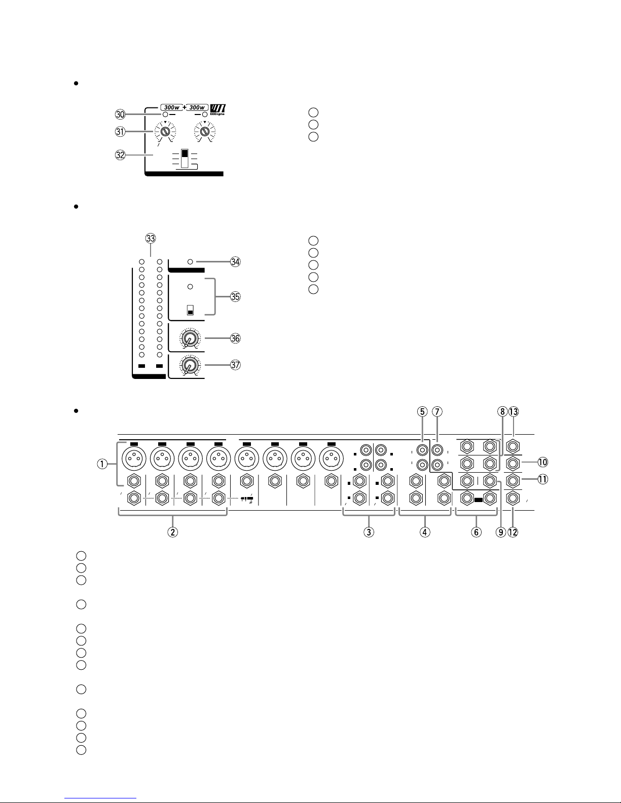
Maximum output power STEREO: 300 W+300 W/4Ω@0.5%THD at 1 kHz
215 W+215 W/8Ω@0.5% THD at 1 kHz
BRIDGE: 600 W/8Ω@0.5%THD at 1 kHz
Frequency response
20 Hz~20 kHz +1 dB, –3 dB
@1 W output into 8Ω
(SPEAKER OUT) Channel Gain control at minimum.
20 Hz~20 kHz +1 dB, –3 dB
@+4 dB output into 600Ω
(ST OUT, MONO OUT, EFFECT
SEND, MONITOR OUT)
Channel Gain control at minimum.
Total harmonic distortion Less than 0.5% @20 Hz~20 kHz, 150 W output into 4Ω(SPEAKER OUT)
Less than 0.3% @20 Hz~20 kHz, +14 dB output into 600Ω
(ST OUT, MONO OUT, EFFECT SEND, MONITOR OUT)
Hum & noise
(Average, Rs=150Ω)
(with 20 Hz~20 kHz BPF)
–128 dB equivalent input noise
–63 dB residual output noise (SPEAKER OUT)
–95 dB residual output noise (ST OUT, MONO OUT, EFFECT SEND, MONITOR OUT)
–87 dB
(ST OUT, MONO OUT) ST master/MONO master fader at maximum level and all
channel fader at minimum.
–64 dB (68 dB S/N)
(ST OUT, MONO OUT) ST master/MONO master fader and 1 channel fader at maxi-
mum level. And 1 channel Gain control at maximum.
–80 dB
(EFFECT SEND, MONITOR OUT) Master fader at maximum level and all channel level control
at minimum.
Maximum voltage gain
91 dB MIC IN to SPEAKER OUT (CH 1~8)
64 dB MIC IN to ST OUT (CH 1~8)
38 dB LINE IN to ST OUT (CH 1~8)
38 dB ST IN to ST OUT (CH 9/10, 11/12)
70 dB MIC IN to EFFECT SEND (CH 1~8)
64 dB MIC IN to MONITOR OUT (CH 1~8)
Crosstalk at 1 kHz –70 dB adjacent input, –70 dB input to output
MIC IN gain control 44 dB variable
POWER AMP level control 14 dB variable
Input channel equalization
HIGH 10 kHz shelving*
MID 2.5 kHz peaking
LOW 100 Hz shelving*
* Turn over/roll off frequency of shelving:3 dB below maximum variable level.
Meters 13 points LED meter
CH peak indicators Red LED on each channel lits when POST EQ signal reaches the level –3 dB below clipping.
Limiter Comp. :THD≥0.5%
LIMIT indicators Turn on THD≥0.5%
Graphic equalizer 7 bands (125, 250, 500, 1k, 2k, 4k, 8k Hz), ±12 dB Maximum
Internal digital effect 16 programs, PARAMETER control
Foot switch Digital effect mute: on/off
Protection circuit (Power amp) POWER switch on/off mute, DC detection,TEMP (heatsink temp. ≥90°C)
Fan circuit stop — low speed (50°C) — variable — high speed (70°C)
Phantom power +48 V is supplied to electrically balanced inputs.
Option FC5 (Foot switch)
Power requirement/
Power consumption
USA and Canada:120V AC 60 Hz, 250 W
Europe: 230 V AC 50 Hz, 300 W
Other: 240 V AC 50 Hz, 300 W
Dimensions (WxHxD) 480
XX
125 454 mm
Weight 16 kg
Accessories Power cord, Owner’s Manual

EMX3000
4
Input terminals Gain
trim Actual load
impedance For use with
nominal
Input level Connectors on mixer
Sensitivity
1
1. Sensitivity is the lowest level that can produce an output of +4 dB (1.23V) or the nominal output level when the unit is set at maximum gain.
(All fader and level controls are at maximum position.)
Max. before clip
MIC INPUT (1–8) MAX
MIN 5 kΩ50~600ΩMics –60 dB (775 µV)
–16 dB (123 mV) –40 dB (7.75 mV)
+4 dB (1.23 V) XLR-3-31 type
2
2. Balanced. (T=HOT, R=COLD, S=GND)
LINE INPUT (1–8) MAX
MIN 50 kΩ
600ΩLines
–34 dB (15.5 mV)
+10 dB (2.45 V) –14 dB (155 mV)
+30 dB (24.5 V) PHONE JACK (TRS)
2
ST INPUT (9–12) MAX
MIN
10 kΩ
–34 dB (15.5 mV)
+10 dB (2.45 V) –14 dB (155 mV)
+30 dB (24.5 V) PHONE JACK
3
3. Unbalanced.
ST SUB IN (1, 2) +4 dB (1.23 V) +20 dB (7.75 V)
TAPE IN (L, R) –10 dBV (316 mV) +10 dBV (3.16 V) PHONO JACK
CH INSERT IN (1–4) 0 dB (775 mV) +20 dB (7.75 V) PHONE JACK (I/O)
4
4. Unbalanced. (T=OUT, R=IN, S=GND)
POWER AMP IN (L, R) +4 dB (1.23 V)
5
5. POWER AMP level control= maximum (+4)
• In these specifications when dB represents a specific voltage, 0 dB is referenced to 0.775 Vrms, 0 dBV is referenced to 1Vrms.
+18 dB (6.16 V)
5
PHONE JACK
3
Output terminals Actual source
impedance For use with
nominal
Output level Connectors on
mixer
Nominal Max. before cliping
ST OUT 1, 2 (L/R)
150Ω600ΩLines +4 dB (1.23 V) +20 dB (7.75 V) PHONE JACK
(TRS)
1
1. Impedance balaned. (T=HOT, R=COLD, S=GND)
MONO OUT
EFFECT SEND
MONITOR OUT 1, 2
REC OUT (L/R) 600Ω10 kΩLines –10 dBV (316 mV) +10 dBV (3.16 V) PHONO JACK
CH INSERT OUT (1–4) 0 dB (775 mV) +20 dB (7.75 V) PHONE JACK (I/O)
2
2. Unbalanced. (T=OUT, R=IN, S=GND)
C-R/PHONES
OUT for PHONES 100Ω40ΩPhones 3 mW 100 mW ST PHONE JACK
3
3. Unbalanced. (T=L, R=R, S=GND)
for C-R OUT 10 kΩLines +4 dB (1.23 V) +20 dB (7.75 V)
SPEAKER OUT 1, 2 (L/R) 0.1Ω4/8ΩSpeaker 300 W/4PHONE JACK
4
4. Unbalanced.
BRIDGE OUT 8ΩSpeaker 600 W/8PHONE JACK
5
5. Balanced. (T=HOT, S=COLD)
• In these specifications when dB represents a specific voltage, 0 dB is referenced to 0.775 Vrms, 0 dBV is referenced 1Vrms.
Input specifications
Output specifications

EMX3000
5

EMX3000
6

EMX3000
7
PANEL LAYOUT
Control Panel
Channel Control Section
PFL PFL
A
B
10
0
10
0
10
0
R
L
+15
-15
GAIN GAIN
MONI 1
MONI 2
EFFECT
PAN
HIGH
MID
LOW
+15
-15
+15
-15
-34
-16 -60
+10 -34
+10
PEAK
10
0
10
0
10
0
R
L
+15
-15
MONI 1
MONI 2
EFFECT
BAL
HIGH
MID
LOW
+15
-15
+15
-15
PEAK
0
5
10
15
20
40
50
25
30
0
5
10
15
20
40
50
25
30
1
910
1
2
3
4
5
6
7
8
9
10
GAIN control
A/B switch (Channels 9/10~11/12 only)
PEAK indicator
Equalizer controls (HIGH, MID, LOW)
Monitor 1/2 controls (MONI 1/2)
Effect control (EFFECT)
PAN (panpot) control (Channels 1~8)
BAL (balance) control (Channels 9/10~11/12)
PFL (pre-fader listen) switch
Channel fader
Stereo Sub Input Section
PFL
10
0
10
0
10
0
10
0
10
0
10
0
MONI 1
MONI 2
ST
MONI 1
MONI 2
ST
ST SUB 2
PFL
ST SUB 1
11
12
13
14
MONI 1 (monitor 1) control
MONI 2 (monitor 2) control
ST (stereo) control
PFL (pre-fader listen) switch

EMX3000
8
15
16
17
18
19
20
Master Control Section
AFLAFLAFLAFLAFL
0
5
10
15
20
40
50
25
30
0
5
10
15
20
40
50
25
30
0
5
10
15
20
40
50
25
30
0
5
10
15
20
40
50
25
30
0
5
10
15
20
40
50
25
30
MONOMONI 2MONI 1 ST 1EFFECT
Tape in Section
TAPE IN
10
0
ST
PFL
Digital effect Section
DIGITAL EFFECT
PARAMETERPROGRAM
8910
3
1
4
2
12
11 1
2
3
4
9
10
11
12
13
14
15
16
5
6
7
8
14
7
16
6
15
13
5
MONI1 MONI2
ON
MAX
MIN
10
0
ST
VOCAL ECHO 1 VOCAL REVERB 1 HALL 1 PLATE 1
PLATE 2
PLATE 3
GATE REVERB
HALL 2
HALL 3
ROOM
VOCAL REVERB 2
VOCAL REVERB 3
VOCAL REVERB 4
VOCAL ECHO 2
VOCAL ECHO 3
VOCAL ECHO 4
10
0
10
0
Graphic equalizer Section
GRAPHIC EQUALIZER
ON
8K4K2K1K500250125
8K4K2K1K500250125
6
0
6
+12
-12
6
0
6
+12
-12
MONI 1 (monitor 1) fader
MONI 2 (monitor 2) fader
EFFECT fader
ST 1 (stereo 1) fader
MONO (monaural) fader
AFL (after fader listen)
21
22
ST (stereo) control
PFL (pre-fader listen) switch
23
24
25
26
27
MONI 1/2 (monitor 1/2) control
ST (stereo) control
PROGRAM selector
ON switch
PARAMETER control
28
29
Graphic equalizer
ON switch

EMX3000
9
1
2
3
4
5
6
7
8
9
10
11
12
13
Power amp Section
POWER AMP
ST1 L
MONI 1
MONO
(BRIDGE)
ST1 R
MONO
LIMITER
LEVEL
BRIDGE
+4
+18 +4
+18
LR
Other indicators and controls
POWER
ST 1
LR
PHANTOM +48V
ON
OFF
C-R/PHONES
ST 2
(1-8ch)
+8
+5
+3
+1
0
-1
-3
-5
-7
-10
-15
-20
10
0
10
0
PEAK
Input/Output pabel
I O I O I O I O
A
A
A
A
B
B
B
B
ST
SUB 1 ST
SUB 2
+4dB +4dB
TAPE REC
ST 1
-10dBV -10dBV
+4dB
ST 2
+4dB +4dB
+4dB
+4dB
+4dB
MONI MONI
MONO
EFFECT
FOOT SW
12
BRIDGE
P.AMP
IN
C-R
PHONES
9 L 11 L L L
LR
LR
RL
9 L
10 R 12 R R R
10 R
11 L
12 R
(MONO) (MONO) (MONO) (MONO)
9 10 11 12
INPUT OUTPUT
L
R
L
R
1
2345678
INSERT
LINE
INSERT
LINE
INSERT
LINE
INSERT
LINE LINE LINE LINE LINE
MIC MIC MIC MIC MIC MIC MIC MIC
INSERT
OUT IN
0dB
I O
30
31
32
LIMITER indicator
LEVEL controls
Power amp select switch
33
34
35
36
37
Peak level indicator
POWER indicator
PHANTOM (+48V) switch and indicator
C-R/PHONES (control room/headphones)control
ST 2 (stereo 2) control
Channel input jacks (MIC, LINE) 1~8
INSERT I/O (insert) jacks 1~4
Channel input jacks 9~12A
Channel input jacks 9~12B
ST SUB 1 (stereo sub 1) jacks
ST SUB 2 (stereo sub 2) jacks
TAPE jacks
P.AMP IN (power amp input) jacks
REC (record) jacks
ST 1 (stereo 1) jacks
ST 2 (stereo 2) jacks
MONI 1 (monitor 1) jack
MONI 2 (monitor 2) jack
MONO (monaural) jack
EFFECT jack
C-R/PHONES (control room/headphones) jack
FOOT SW (foot switch) jack

EMX3000
10
Rear panel
AC IN
21 21
BRIDGE
ON OFF
R/
MONO
L/
MONI1
SPEAKERS
POWER
1
2
3
CIRCUIT BOARD LAYOUT
PFL
10
0
10
0
10
0
10
0
10
0
10
0
MONI 1
MONI 2
ST
MONI 1
MONI 2
ST
ST SUB 2
PFL
ST SUB 1
AFLAFLAFLAFLAFL
0
5
10
15
20
40
50
25
30
0
5
10
15
20
40
50
25
30
0
5
10
15
20
40
50
25
30
0
5
10
15
20
40
50
25
30
0
5
10
15
20
40
50
25
30
MONOMONI 2MONI 1 ST 1EFFECT
TAPE IN
10
0
ST
PFL
DIGITAL EFFECT
PARAMETERPROGRAM
8910
3
1
4
2
12
11 1
2
3
4
9
10
11
12
13
14
15
16
5
6
7
8
14
7
16
6
15
13
5
MONI1 MONI2
ON
MAX
MIN
10
0
ST
VOCAL ECHO 1 VOCAL REVERB 1 HALL 1 PLATE 1
PLATE 2
PLATE 3
GATE REVERB
HALL 2
HALL 3
ROOM
VOCAL REVERB 2
VOCAL REVERB 3
VOCAL REVERB 4
VOCAL ECHO 2
VOCAL ECHO 3
VOCAL ECHO 4
10
0
10
0
GRAPHIC EQUALIZER
ON
8K4K2K1K500250125
8K4K2K1K500250125
6
0
6
+12
-12
6
0
6
+12
-12
POWER AMP
ST1 L
MONI 1
MONO
(BRIDGE)
ST1 R
MONO
LIMITER
LEVEL
BRIDGE
+4
+18 +4
+18
LR
POWER
ST 1
LR
PHANTOM +48V
ON
OFF
C-R/PHONES
ST 2
(1-8ch)
+8
+5
+3
+1
0
-1
-3
-5
-7
-10
-15
-20
10
0
10
0
PEAK
PFL
A
B
GAIN
-34
+10
10
0
10
0
10
0
R
L
+15
-15
MONI 1
MONI 2
EFFECT
BAL
HIGH
MID
LOW
+15
-15
+15
-15
PEAK
0
5
10
15
20
40
50
25
30
PFL
A
B
GAIN
-34
+10
10
0
10
0
10
0
R
L
+15
-15
MONI 1
MONI 2
EFFECT
BAL
HIGH
MID
LOW
+15
-15
+15
-15
PEAK
0
5
10
15
20
40
50
25
30
11 129 10
PFL
10
0
10
0
10
0
R
L
+15
-15
GAIN
MONI 1
MONI 2
EFFECT
PAN
HIGH
MID
LOW
+15
-15
+15
-15
-34
-16 -60
+10
PEAK
0
5
10
15
20
40
50
25
30
PFL
10
0
10
0
10
0
R
L
+15
-15
GAIN
MONI 1
MONI 2
EFFECT
PAN
HIGH
MID
LOW
+15
-15
+15
-15
-34
-16 -60
+10
PEAK
0
5
10
15
20
40
50
25
30
PFL
10
0
10
0
10
0
R
L
+15
-15
GAIN
MONI 1
MONI 2
EFFECT
PAN
HIGH
MID
LOW
+15
-15
+15
-15
-34
-16 -60
+10
PEAK
0
5
10
15
20
40
50
25
30
PFL
10
0
10
0
10
0
R
L
+15
-15
GAIN
MONI 1
MONI 2
EFFECT
PAN
HIGH
MID
LOW
+15
-15
+15
-15
-34
-16 -60
+10
PEAK
0
5
10
15
20
40
50
25
30
PFL
10
0
10
0
10
0
R
L
+15
-15
GAIN
MONI 1
MONI 2
EFFECT
PAN
HIGH
MID
LOW
+15
-15
+15
-15
-34
-16 -60
+10
PEAK
0
5
10
15
20
40
50
25
30
PFL
10
0
10
0
10
0
R
L
+15
-15
GAIN
MONI 1
MONI 2
EFFECT
PAN
HIGH
MID
LOW
+15
-15
+15
-15
-34
-16 -60
+10
PEAK
0
5
10
15
20
40
50
25
30
PFL
10
0
10
0
10
0
R
L
+15
-15
GAIN
MONI 1
MONI 2
EFFECT
PAN
HIGH
MID
LOW
+15
-15
+15
-15
-34
-16 -60
+10
PEAK
0
5
10
15
20
40
50
25
30
PFL
10
0
10
0
10
0
R
L
+15
-15
GAIN
MONI 1
MONI 2
EFFECT
PAN
HIGH
MID
LOW
+15
-15
+15
-15
-34
-16 -60
+10
PEAK
0
5
10
15
20
40
50
25
30
12345678
I O I O I O I O A
A
A
A
B
B
B
B
ST
SUB 1 ST
SUB 2
+4dB +4dB
TAPE REC
ST 1
-10dBV -10dBV
+4dB
ST 2
+4dB +4dB
+4dB
+4dB
+4dB
MONI MONI
MONO
EFFECT
FOOT SW
12
BRIDGE
P.AMP
IN C-R
PHONES
9 L 11 L L L
LR
LR
RL
9 L
10 R 12 R R R
10 R
11 L
12 R
(MONO) (MONO) (MONO) (MONO)
9 10 11 12
INPUT OUTPUT
L
R
L
R
12345678
INSERT
LINE
INSERT
LINE
INSERT
LINE
INSERT
LINE LINE LINE LINE LINE
MIC MIC MIC MIC MIC MIC MIC MIC
INSERT
OUT IN
0dB
I O
MAIN
MAIN
DSP
DSP
2/3PWR2
2/3PWR2
1/3PWR2
1/3PWR2
3/3PWR2
3/3PWR2
PWR1
PWR1
SPEAKERS (speaker output) jacks
POWER switch
AC inlet

EMX3000
11
Units: mm
DIMENSIONS
168
W: 480
D: 454
H: 125
286
CNM01
12pin
13pin
2pin
4pin
6pin
13pin
3pin
3pin
3pin
3pin
12pin
CNM04
CN103
CN105
CN106
CN104
CN101
CN102
CN102
CN301
CN101
MAIN
DSP
PWR1
PWR2 3/3 PWR2 2/3
PWR2 1/3
Power transformer
AC INLET
DC fan
Location
1
2
3
4
5
DSP-PWR1
MAIN-PWR1
MAIN-DSP
PWR1-PWR2 2/3
PWR1-PWR2 3/3
2426&2426 3P 210L
2426&2426 12P
2426&2426 13P
B&C #18 4P
B&C #18 3P
(V705810)
(V705820)
(V705830)
(V702070)
(V702080)
Connector Assembly Remarks Parts No.
2
2
3
3
1
4
4
5
5
1
WIRING

EMX3000
12
IC101,201,301,401IC102, IC302
IC502,IC702
IC104,304
IC103,303
12
2
6
5
5
IC501,601,701,801
6
5
7
(3) (1)
7
IC504,704
IC504, IC704
9ch: IC901, IC902
11ch: IC801, IC802
10ch: IC901, IC902
12ch: IC801, IC802
9ch: IC903
11ch: IC803
10ch: IC903
12ch: IC803
9ch: IC904
11ch: IC804
10ch: IC904
12ch: IC804
6
(2) (1)
7
6
(2) (1)
7
57 57
ST SUB1: ICD01
ST SUB2: ICD02
31
57
ST SUB1: ICD01
ST SUB2: ICD02
31
ICD03
57
ICD03
31
31
57
ICE01 ICE02
6721
ICH01
67
ICH01
21
ICJ01
21
ICK01
67
ICK01
21
ICF01
6721
7
2
4
4
3
3
1
1
2
4
3
1
2
4
3
12
4
31
2
4
31
2
4
31
3
12
3
MAIN
CN101-1
CNM04-1
CN101CN101-2
CN101-4~8
CN101-9~11
CNM0
4
A
A
CNM04-1
CNM04-9~11
CNM04-4~8
BLOCK & LEVEL DIAGRAM

EMX3000
13
1
ICE02
ICF02
ICE04
57
ICE03
57
ICE03
31
ICJ01
CNM01-8
CNM01-10
CN102-10 RY102
RY101
CN102-8 CN103-1
CN103-3
1+
2+
76
ICG01
67
ICG01
21
ICH02
67
ICH02
21
ICJ02
67
ICK02
21
ICK02
67
ICE04
31
ICM01
3
ICM02
3
1
1
2/3
PWR2
PWR1
DSP
CN101-1
CNM04-1
CN101-12 CNM04-12
CN101-13 CNM04-13
CN101-3CN101-2
CN101-4~8
CN101-9~11
CNM04-2
A
A
CNM04-1
1

EMX3000
14
DISASSEMBLY PROCEDURE
Fig.1
[90]: Bind Head Tapping Screw-B 3.0 X 6 MFZN2BL (EP600230)
[100]: Bind Head Tapping Screw-B 3.0 X 6 MFZN2BL (EG340190)
1. Panel Assembly and Bottom Assembly (Manhour
requirement: 5 min.)
1-1. After removing the six (6) screws marked [90] and six
(6)screwsmarked[100],lifttherearsideoftheassembly
and remove it from claws on the front.(Fig.1)
2. MAINCircuitBoard(Manhourrequirement:30min.)
2-1. Remove the panel assembly and the bottom
assembly.(See Procedure 1.)
2-2. Remove the three (3) screws marked [P70] from
each side (front and rear).The shield plate can then
be removed. (Fig. 2)
2-3. Remove all the knobs from the front panel and all
the special hexagon nuts from the jacks.
2-4. Remove the fourteen (14) screws marked [P40] and
eighteen (18) screws marked [P50] (cannon
connector, pin jack).The MAIN circuit board can then
be removed. (Fig. 2)
[100]
[90] [90]
[100]

EMX3000
15
Fig.2
[P40]: Flat Head Tapping Screw-B 3.0 X 25 MFZN2BL (VV095300)
[P50]: Bonding Screw-B 3.0 X 8 MFZN2BL (VN413300)
[P70]: Bind Head Tapping Screw-B 3.0 X 6 MFZN2BL (EP600230)
3. PWR1 CircuitBoard(Manhourrequirement:30 min.)
3-1. Remove the panel assembly and the bottom
assembly.(See Procedure 1.)
3-2. Remove the four (4) screws marked [B130] and
remove the PWR1 circuit board together with the
isolation sheet. (Fig. 3)
3-3. Remove the twenty-eight (28) screws marked
[B60]and four (4) screws marked [B50].The PWR1
circuit board can then be separated from the isolation
sheet. (Fig. 3)
4. DSP Circuit Board (Manhour requirement:10 min.)
4-1. Remove the panel assembly and the bottom
assembly.(See Procedure 1.)
4-2. Remove each PCB support at four (4) locations.The
DSP circuit board can then be removed. (Fig. 3)
5. PWR2 3/3 Circuit Board (Manhour requirement:
10 min.)
5-1 Remove the panel assembly and the bottom
assembly.(See Procedure 1.)
5-2. Remove the one (1) screw marked [B75] and the
electrolytic capacitor holder.The PWR2 3/3 circuit
board can then be removed. (Fig. 3)
6. DC fan (Manhour requirement: 10 min.)
6-1. Remove the panel assembly and the bottom
assembly.(See Procedure 1.)
6-2. Remove the two (2) screws marked [B100].The DC
fan can then be removed.(Fig. 3)
[P40]
[P70] [P70] [P70]
[P70]
[P40]
MAIN
[P40]
[P40]
[P40]
[P70]
[P50]
[P40]
[P70][P70] [P50]
[P50]

EMX3000
16
8. PWR2 2/3 Circuit Board (Manhour requirement:
15 min.)
8-1. Remove the panel assembly and the bottom
assembly.(See Procedure 1.)
8-2. Remove the five (5) special hexagonal nuts and one
(1) screw marked [R30] from the rear panel.The
PWR2 2/3 circuit board can then be remove.(Fig.4)
9. PWR2 1/3 Circuit Board (Manhour requirement:
15 min.)
9-1. Remove the panel assembly and the bottom
assembly.(See Procedure 1.)
9-2. Remove the two (2) screws marked [R60], PSW
knob, PSW escussion and the 2 screws marked
[R20]. The PWR2 1/3 circuit board can then be
removed.
Fig.3 [B50]:Bind Head Screw SP 3.0 X 8 MFZN2Y (FG330290)
[B60]:Pan Head Screw SPK 3.0 X 12 MFZN2Y (VJ470900)
[B75]:Bind Head Tapping Screw-B 3.0 X 6 MFZN2BL (EP600230)
[B100]:Bind Head Tapping Screw-B 4.0 X 8 MFZN2BL (EG340190)
[B130]:Bind Head Tapping Screw-B 4.0 X 8 MFZN2BL (EG340190)
7. Power transformer (Manhour requirement:10 min.)
7-1. Remove the panel assembly and the bottom
assembly.(See Procedure 1.)
7-2. Remove the hexagonal bolt.The power transformer
can then be removed. (Fig. 3)
(See Fig.3 for drawing direction of wiring assembly.)
Fig.4 [R20]:Bind Head Screw 3.0 X 8 MFZN2BL (VB659000)
[R30]:Bonding Screw-B 3.0 X 8 MFZN2BL (EG413300)
[R60]:Bind Head Tapping Screw-B 4.0 X 8 MFZN2BL (EG340190)
PSW1
DSP PWR2 3/3
[B50]
[B130]
[B130]
[B130]
[B75]
[B130]
[B60]
[B60]
[B60]
[B50]
[B100]
[B60]
[B60]
Power transformer
DC fan
PCB support
PWR2 2/3
PWR2 1/3
[R60] [R30]
[R20] PSW knob [R20]
PSW escussion
Hexagonal nut

EMX3000
17
LSI PIN DESCRIPTION
PIN
No. NAME I/O FUNCTION
PIN
No. NAME I/O FUNCTION
1
2
3
4
5
6
7
8
9
10
11
12
13
14
15
16
17
18
19
20
21
22
23
24
25
26
27
28
29
30
31
32
33
34
35
36
37
38
39
40
41
42
43
44
45
46
47
48
49
50
51
52
53
54
55
56
57
58
59
60
61
62
63
64
65
66
67
68
69
70
71
72
73
74
75
76
77
78
79
80
81
82
83
84
85
86
87
88
89
90
91
92
93
94
95
96
97
98
99
100
ED2
ED3
ED4
ED5
ED6
ED7
VSS
VDD
CLKM0
CLKM1
TMS
TDI
TCK
CLKIN
VSS
VDD
CLKO
EA12/ED8
EA13/ED9
EA14/ED10
EA15/ED11
VSS
VDD
EA16/ED12
EA17/ED13
EA18/ES14
EA19/ED15
EA4/ED16
EA5/ED17
EA6/ED18
EA7/ED19
VSS
VDD
EA8/ED20
EA9/ED21
EA10/ED22
EA11/ED23
TEST0
TEST1
TEST2
TEST3
/BIO
/INT1
ARBC1
ARBC2
AX1
AX2
AX3
VSS
VDD
HX/SDA
/EMPTY
AXLR2
AR1
AR2
HRBCK/SA0
HR/SA1
HRS/SA2
VSS
VDD
HXBCK/SCL
HXS/SA3
/CS/SA4
HBCKS/SA5
I2CSEL
VSS
VDD
AXBC1
AXBC2
AXLR1
DIVS
/LAV
/LMV
/DRDY
EMU0
EMU1
TDO
DIV512
ARLR1
ARLR2
HDIR/SA6
SEL5V3V
/MUTE
/TRST
/RS
VSS
VDD
/IOE
/RAS/SRCS
/CAS/SROE
/ROME
/WE
EA0
EA1
EA2
EA3
VSS
VDD
ED0
ED1
I/O
I/O
I/O
I/O
I/O
I/O
S
S
I
I
I
I
I
I
S
S
O
I/O
I/O
I/O
I/O
S
S
I/O
I/O
I/O
I/O
I/O
I/O
I/O
I/O
S
S
I/O
I/O
I/O
I/O
I
I
I
I
I
I
I
I
O
O
O
S
S
I/O/Z
O/Z
I
I
I
I
I
I
S
S
I
I
I
I
I
S
S
I
I
I
O
O
O
O/Z
I/O/Z
I/O/Z
O/Z
O
I
I
I
I
I
I
I
S
S
O
O
O
O
O
O
O
O
O
S
S
I/O
I/O
ZFX-2 (XY297A00)CPU DSP: IC105
External Memory and I/O Data Bus
Ground
Power Supply
Clock Mode
TAP(Test Access Port) Mode Select
TAP Data Input
TAP Clock
Master Clock
Ground
Power Supply
Machine Clock Output
External SRAM and ROM Address Bus/
External DRAM and I/O Data Bus
Ground
Power Supply
External SRAM and ROM Address Bus/
External DRAM and I/O Data Bus
External Memory Address Bus/ External I/O
Data Bus
Ground
Power Supply
External Memory Address Bus/ External I/O
Data Bus
Test Mode Control
Separate Control Input
Interrupt 1
Audio Data Receive Unit 1 bit Clock
Audio Data Receive Unit 2 bit Clock
Audio Data Transmitt Unit 1 Data Output
Audio Data Transmitt Unit 2 Data Output
Audio Data Transmitt Unit 3 Data Output
Ground
Power Supply
Host Interface Data Output/I2C Bus Data
CMEM Update Buffer and HR Resistor Empty Flag Output
Audio Data Transmitt Unit 2/3 Left and
Right Channel Frame Frequency Signal
Audio Data Receive Unit 1 Data Input
Audio Data Receive Unit 2 Data Input
Host Interface Receive Clock / I2C Bus Address 0
Host Interface Data Input/ I2C Bus Address 1
Host Interface Receive Data Frame
Frequency Signal/ I2C Bus Address 2
Ground
Power Supply
Host Interface Transmitt Clock/ I2C Bus Clock
Host Interface Transmitt Data Frame
Frequency Signal/ I2C Bus Address 3
Host Interface Chip Select/ I2C Bus Address 4
HRBCK/HXBCK Active Edge Select/ I2C Bus Address 5
Host Interface Mode Select
Ground
Power Supply
Audio Data Transmitt Unit 1 bit Clock
Audio Data Transmitt Unit 2/3 bit Click
Audio Data Transmitt Unit 1 Left and Right
Channel Frame Frequency Signal
Machine Clock Output then 8 min.
Ruch ALU Overflow Frag Output
Ruch MAC Overflow Frag Output
Host Interface Transmitt Data Ready Frag Output
Emurator Interrupt 0
Emurator Interrupt 1
TAP(Test Access Port) Data Output
Machine Clock then512 min.
Audio Data Receive Unit 1 Left and Right
Channel Frame Frequency Signal
Audio Data Receive Unit 2 Left and Right
Channel Frame Frequency Signal
Host Interface Data Format Select/ I2C Bus Address 6
Input Level Control
Mute Control
TAP(Test Access Port) Reset
Hardware Reset
Ground
Power Supply
External I/O Enable
External DRAM Low Address Strove/External
SRAM Chip Select
External DRAM Culumn Address Strove/External
SRAM Output Enable
External ROM Enable
External Memory and I/O Wright Enable
External Memory and I/O Address Bus
Ground
Power Supply
External Memory and I/O Data Bus
CLKM0
CLKM1
1
0
0
3
1
0
6
0
1
PLL BYPASS
1
1

EMX3000
18
PIN
No. NAME I/O FUNCTION
PIN
No. NAME I/O FUNCTION
1
2
3
4
5
6
7
8
9
10
11
12
13
14
15
16
17
18
19
20
21
22
23
24
25
26
27
28
VINL
Vcc1
AGND1
VREFL
VREFR
VINR
CINPR
CINNR
CINNL
CINPL
VCOM
VOUTR
AGND2
Vcc2
VOUTL
LRCIN
BCKIN
DIN
DOUT
XTI
XTO
CLKIO
VDD
DGND
FMT2
FMT1
FMT0
RSTB
I
I
O
O
I
I
I
O
I
O
I/O
I
I
I
I
PCM3001E/2K(X0053A00) ADA
DSP: IC104
ADC Analog Input, Lch
ADC Analog Power Supply
ADC Analog GND
ADC Reference decouple, Lch
ADC Reference Decouple, Rch
ADC Analog Input, Rch
ADC Anti-areasing Filter Capacitor (+), Rch
ADC Anti-areasing Filter Capacitor (-), Rch
ADC Anti-areasing Filter Capacitior (-), Lch
ADC Anti-areasing Filter Capacitor (+), Rch
DAC Center Voltage Decouple
DAC Analog Output, Rch
DAC Analog GND
DAC Analog Power Supply
DAC Analog Output, Lch
Sampling Clock Input (fs)
Bit Clock Input
Audio Data Input
Audio Data Output
Crystal Oscillator Input, External System Clock Input
Crystal Oscillator Output
Crystal Oscillator Buffer Output, External System Clock Input
Digital Power Supply
Digital GND
Audio Data Format 2 (Pull up to 70k ohm typical)
Audio Data Format 1 (Pull up to 70k ohm typical)
Audio Data Format 0 (Pull up to 70k ohm typical)
Reset Input, Active "L" (Pull up to 70k ohm typical)
PIN
No.
NAME I/O FUNCTION
PIN
No.
NAME I/O FUNCTION
1
2
3
4
5
6
7
8
9
10
11
12
13
14
15
16
17
18
19
20
21
22
23
24
25
26
27
28
29
30
31
32
33
34
35
36
37
38
39
40
41
42
43
44
P12/ANI2
P13/ANI3
P14/ANI4
P15/ANI5
P16/ANI6
P17/ANI7
P72/SCK2/ASCK
P71/SO2/TXD
P70/SI2/RXD
P101/T16/T06
P100/T15/T05
P50
P51
P52
P53
P54
VSS
P55
P56
P57
P30
P31
NC
P32
P33
P34
P35/PCL
P36/BUZ
P37
P00
P01/INTP1
P02/INTP2
P03/INTP3
NC
RESET
IC(VPP)
X2
X1
VDD
AVDD
AVREF
AVSS
P10/ANI0
P11/ANI1
I/O
I/O
I/O
I/O
I/O
I/O
I/O
I/O
I/O
I/O
I/O
I/O
I/O
I/O
I/O
I/O
I/O
I/O
I/O
I/O
I/O
I/O
-
I/O
I/O
I/O
I/O
I/O
I/O
I
I/O
I/O
I/O
-
I
-
-
I
-
-
I
-
I/O
I/O
8 bits input/output port./A/D converter analog input.
Port 7. 3 bits input/output port./Serial clock
input/output of serial interface./Serial clock
input for asynchronus serial interface.
Port 7. 3 bits input/output port./Serial data output for serial
interface./Serial data output for asynchronus serial interface.
Port 7. 3 bits input/output port./Serial data input of serial
interface./Serial data input for asynchronus serial interface
Port 10. 2 bits input/output port./External count
clock input to 8 bits timer(TM6)./8 bits timer output.
Port 10. 2 bits input/output port./External count
clock input to 8 bits timer(TM5)./8 bits timer output.
Port 5. 8 bits input/output port.
Port 3. 8 bits input/output port.
Not connect.
Port 3. 8 bits input/output port.
Port 3. 8 bits input/output port./Clock output.
Port 3. 8 bits input/output port./Buzzer output.
Port 3. 8 bits input/output port.
Input only
4 bits input/output port./Effective edge (Rising
edge, falling edge, both rising and falling
edges) specifiable external interrupt input.
4 bits input/output port./Effective edge (Rising
edge, falling edge, both rising and falling
edges) specifiable external interrupt input.
4 bits input/output port./Effective edge (Rising
edge, falling edge, both rising and falling
edges) specifiable external interrupt input.
Not connect
System reset input
Internal connect
Main system clock oscillator X'tal
Power Supply
A/D Converter Analog Power Supply
A/D Converter Power Supply Input
A/D Converter ground
8 bits input/output port./A/D converter analog input.
UPD78082(XZ312A00) MCU
DSP: IC102

EMX3000
19
IC BLOCK DIAGRAM
74HCU04DT(XZ110A00)
INVERTER
1
1A
2
3
4
5
6
7
1Y
2A
2Y
3A
3Y
V
SS
8
9
10
11
12
13
14
VDD
6A
6Y
5A
5Y
4A
4Y
M5229P (XG203A00)
7-SEG. GRAPHIC
MAIN: ICE02, ICF02
1
2
3
4
5
6
7
8
9
10 11
12
13
14
15
16
17
18
19
20
IN1
IN2
IN3
IN4
IN5
NF1
NF2
NF3
NF4
NF5
-Vcc
GND
+Vcc
OUTPUT
INVERTED
INPUT
NON-INVERTED
INPUT
NF7
NF6
IN7
IN6
-+
-+
-+
-+
-+
-+
-+
-+
47k
560
47k
560
47k
560
47k
560
47k
47k
47k
47k
560
10k
10k
BA682A
(
XS046A00
)
LED LEVEL METER
MAIN: ICM01, ICM02
NJM4558MT-1
(
IG103520
)
OP AMP
DSP: IC103
NJM2068L-D
(
XM356A00
)
OP AMP
MAIN: IC101–104, IC201, IC301–IC304,
IC401, IC501–IC504, IC601,
IC701–704, IC801, IC901–904,
ICB01–04, ICD01–03, ICE01,
ICH01, ICJ01,ICK01
NJM4558L-D
(
XQ212A00
)
OP AMP
PWR1: IC101, IC201
NJM4580L
(
XF195A00
)
OP AMP
MAIN:
ICE03, ICE04, ICG01, ICH02, ICJ02
NJM4556AL
(
XP844A00
)
OP AMP
MAIN: ICK02
1
A
2345678
IN V
+IN
OUT
AAA +VIN
+IN OUT
BBB
+
B
+
BA682A
2 2 2 2
117 16 15 14 13 12 11 10 876 5
Vreg
reg
V
Vcc Vc1 Vc2 Vc3 Vc4 Vc5 Vc6 Vc7 Vc8 Vc9 Vc10 Vc11 Vc12
3
4918 2
to R :Set I LEDGNDGND
INPUT
1
to R3, C2 :
Discharge Constant
Output A
Inverting
Input A
Non-Inverting
Input A
DC Voltage
Supply
DC Voltage
Supply
Output B
Inverting
Input B
Non-Inverting
Input B
1
2
3
4
8
7
6
5
V
DSP: IC101

EMX3000
20
A
INPUT
A
MIC
LINE
INSERT
GAINGAINGAIN
HIGHHIGHHIGH
MIDMIDMID
LOWLOWLOW
MONI 1MONI 1MONI 1
MONI 2MONI 2MONI 2
EFFECTEFFECT
PANPANPAN
PFLPFLPFLPFLPFLPFLPFLPFLPFL PF
L
PANPANPAN PANPANPAN PANPANPAN PANPANPAN PANPANPAN PANPANPAN PANPANPAN BALBALBAL BALBALBAL
EFFECTEFFECTEFFECT EFFECTEFFECT EFFECTEFFECTEFFECT EFFECTEFFECTEFFECT EFFECTEFFECTEFFECT EFFECTEFFECTEFFECT EFFECTEFFECTEFFECT EFFECTEFFECTEFFECT EFFECTEFFECTEFFECT
MONI 2MONI 2MONI 2 MONI 2MONI 2MONI 2 MONI 2MONI 2MONI 2 MONI 2MONI 2MONI 2 MONI 2MONI 2MONI 2 MONI 2MONI 2MONI 2 MONI 2MONI 2MONI 2 MONI 2MONI 2MONI 2 MONI 2MONI 2MONI 2
MONI 1MONI 1MONI 1 MONI 1MONI 1MONI 1 MONI 1MONI 1MONI 1 MONI 1MONI 1MONI 1 MONI 1MONI 1MONI 1 MONI 1MONI 1MONI 1 MONI 1MONI 1MONI 1 MONI 1MONI 1MONI 1 MONI 1MONI 1MONI 1
LOWLOWLOW LOWLOWLOW LOWLOWLOW LOWLOWLOW LOWLOWLOW LOWLOWLOW LOWLOWLOW LOWLOWLOW LOWLOWLOW
MIDMIDMID MIDMIDMID MIDMIDMID MIDMIDMID MIDMIDMID MIDMIDMID MIDMIDMID MIDMIDMID MIDMIDMID
HIGHHIGHHIGH HIGHHIGHHIGH HIGHHIGHHIGH HIGHHIGHHIGH HIGHHIGHHIGH HIGHHIGHHIGH HIGHHIGHHIGH HIGHHIGHHIGH
GAINGAINGAIN GAINGAINGAIN GAINGAINGAIN GAINGAINGAIN GAINGAINGAIN GAINGAINGAIN GAINGAINGAIN GAINGAINGAIN
I/O
1
INSERT
I/O
2
INSERT
I/O
3
INSERT
I/O
4
5678
LINE LINE LINE LINE LINE LINE LINE
MIC MIC MIC MIC MIC MIC MIC
9L
10R
11L
12R
9L
10R
9/10 11/12
11L
12R
GAINGAINGAIN
HIGHHIGHHIGH
CIRCUIT BOARDS
MAIN Circuit Board
Other manuals for EMX3000
3
Table of contents
Other Yamaha Recording Equipment manuals

Yamaha
Yamaha MDR-3 User manual

Yamaha
Yamaha TG-33 User manual

Yamaha
Yamaha QY10 Manual

Yamaha
Yamaha GEP50 User manual

Yamaha
Yamaha SPX1000 User manual

Yamaha
Yamaha CRD-HD1300 User manual

Yamaha
Yamaha YRM-502 User manual

Yamaha
Yamaha QY 300 User manual

Yamaha
Yamaha FX900 User manual

Yamaha
Yamaha QY20 User manual

Yamaha
Yamaha NAI48-ES User manual

Yamaha
Yamaha EMT-10 User manual

Yamaha
Yamaha EME-1 User manual

Yamaha
Yamaha MW10 User manual

Yamaha
Yamaha ACD1 User manual

Yamaha
Yamaha GEP50 User manual

Yamaha
Yamaha D1030 User manual

Yamaha
Yamaha TX16W User manual

Yamaha
Yamaha SPX900 User manual

Yamaha
Yamaha VCJ5740 User manual