Zenith SM-Z-89 User manual

SM-Z-B9/90
Computer
System
Service
Manual
2.I'N
data
~
systems
ZENITH DATA SYSTEMS
SAINT JOSEPH, MICHIGAN 49085
585-7
Copyright ©1982
Zenith Data Systems
All Rights Reserved
Printed in the United States of America

The
Z-89/90 Computer
System
This
Z-89/90 ComputerSystem Service
Manual
contains
service
information
for
the
following six
Zenith
Data Systems products:
1.
The
Z-89/90 Computers.
2.
The
Z-89-37 Double-Density Disk Controller.
3.
The
H-88-1 Single-Density Disk Controller.
4.
The
H-17-1
Floppy
Disk Drive.
5.
The
H-17-4
Floppy
Disk Drive.
6.
The
WH-88-16
Memory
Expansion.
T

Z-89/90
Computers
Service
Manual
ZENITH
DATA
SYSTEMS
SAINT
JOSEPH,
MICHIGAN
49085
I I
585-7
Copyright ©1982
Zenith Data Systems
All Rights Reserved
Printed in the United Statee of America

nl
COMPUTER
Table
of
Contents
SPECIFICATIONS 1-1
CPU Boards Z-89/90 , , 1-2
SETUP AND TESTING
2-1
Power Line Considerations
,.........
2-1
Cabinet Removal ,2-2
ZDS SYSTEM CONFIGURATION , .
..
3-1
Terminal Logic Circuit Board 3-1
CPU Logic Circuit Board 3-4
Serial Interface 3-20
Memory
Map
3-22
I/O Port Usage 3-22
OPERATION "4-1
Command
Summary
4-1
Keyboard
Operation.
. . . . . . . . . . . . . . . . . . . .
..
4-3
Normal Modes
and
Keys
.,
4-5
CIRCUIT DESCRIPTION 5-1
Power
Supply
Circuit
B~~~d'
:::::::::::::
::
5-2
Video Deflection Circuit Board 5-3
Video Driver Circuit Board
:::::::::::::
5-6
Terminal Logic Circuit Board 5-6
CPU Logic Circuit Board 5-15
Serial Interface I/O Circuit Board 5-21
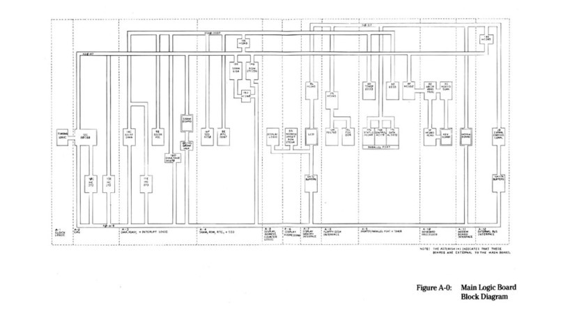
Block Diagrams fold-outs
SERVICE ,6-1
CRT
Adjustment
6-2
Switch
Configurations 6-4
CPU Logic Circuit Board 6-6
Rotational
Speed
Test 6-22
Memory Testing
..
, , 6-23
Troubleshooting Charts 6-25
CIRCUIT BOARD X-RAY VIEWS
7-1
SEMICONDUCTOR IDENTIFICATION CHARTS 8-1
Component
Number
Index
,8-1
Part
Number
Index
8-4
REPLACEMENT PARTS LIST 9-1
Power
Supply
9-1
Video Deflection Circuit Board 9-1
Video
Driver Circuit Board 9-3
Terminal Logic Circuit Board 9-3
CPU Logic Circuit Board 9-4
Chassis Parts 9-5
Serial Interface I/O Circuit
Board.
. . . . . . . .
..
9-6
SCHEMATIC DIAGRAMS fold-in

COMPUTER
11-1
Specificalions
CPU
AND
MEMORY
Processor .
Clock .
Memory .
DISPLAY
CRT
.
Display Format .
Display Size .
Character Size .
Character
Type
.
Keyboard .
Cursor .
Cursor Controls .
Cursor
Addressing
.
Tab .
Refresh Rate .
Edit
Functions
.
Erase
Functions
.
Bell .
Video .
Z-80.
2.048 MHz.
48K bytes
user
RAM
(expandable
to
64K), Z-89 series
64K bytes
user
RAM, Z-90 series
8K
System
for ROM
and
RAM. 8K reserved.
12" diagonal -green
phosphor.
24 lines of 80 characters (with access
to
25th line).
6.5"
high
x8.5" wide.
0.2"
high
x0.1"
wide
(approximate).
5 x 7
dot
matrix
(upper
case); 5 x 9
dot
matrix
(lower
case
with
descenders); 8 x 10
dot
matrix
(graphics).
84 keys (60
alphanumeric,
12 function/control)
plus
a
12-key
numeric/control
pad.
Blinking,
nondestructive,
underline,
block, or dis-
abled
(DIP
switch
selectable).
Up,
down,
left, right,
home,
CR,
LF,
back
space, tab,
and
cursor off.
Relative
and
direct.
Standard
8-column
tab.
60 Hz at 60 HZ/50 Hz at
50
Hz
line
frequency.
Insert
and
delete character or line.
Erase page, erase to
end
of line,
and
erase
to
end
of
page.
Audible
alarm
on
receipt
of ASCII
BEL.
Normal
and
reverse by character.

1-
21
COMPUTER
SERIAL
INTERFACE
Channels.
'" " .
Output
Levels .
Input
Levels .
Character Length .
Parity .
Stop Bits .
Baud Rates .
GENERAL
Power
Requirements .
Size .
Weight .
Operating
Temperature
.
Storage
Temperature
.
3
EIA
RS-232C.
Each
channel
provides serial
data
and
primary
RS-
232C
handshake.
RS-232C.
RS-232C compatible.
5,6,7,
or 8bits.
Even, odd, stick, or none.
1,
1-1/2 or
2.
All
standard
rates
to
57,600 baud.
115/230 volts at 90
watts
max.
13"
high
x
17"
wide
x
20"
deep
(3:3
x43.2 x50.8 em).
46 lbs. (20.7 kg).
10° to 35° Celsius.
0°
to 50° Celsius.
CPU BOARDS
Z·89/90
The
CPU boards for
the
Z-89 (HE 181-3396)
and
the
Z-90
(HE
181-3615) are basically
the
same,
with
the
following exceptions:
Z-89
Z-90
IC
U516
HE 444-41
HE 444-83
IC
U518
HE 444-62
HE 444-84
IC
U549
HE
443-904
See
note
1.
IC
U557
HE
443-912
See
note
2.
IC
U558
HE 443-754
HE 100-1817
NOTE
1:
The
memory
chip
is left
out
to receive
the
cable from
the
16K Memory
Expansion
Board.
NOTE
2:
U557 is left
open
to
receive
the
interface cable from
the
Z-89-37 Controller Board.
The
Z-90 CPU boardhas
the
JJ505
jumper
plug
removed. Cable (HE 134-1159) is
connected
from JJ505
to
Pin
14 of P508,
to
enable
the
4K ROM
at
U518.
JJ501
must
be
jumpered
for correct
memory
size (48K or 64K).
Theseboardsmay be
interchanged
if
the
above modificationsare made.
The
Z-90 CPU
board
may
be
used
as
a
direct
replacement
if
the
proper
IC's are
inserted
at
U549, U557,
and
U558. U516
and
U518
do
not
have
to
be
changed.
Zenith
Data Systemsreserves
the
right
to
discontinue
products
and
to
change
specifications
at
any
time
without
incurring
any
obligation
to
incorporate
new
features
in
products
previously sold.

COMPUTER,
12-1
Setup
and
l'esting
POWER LINE CONSIDERATIONS
If
you
need
to
change
the
position
of
the
115/230
switch (located
on
the
bottom of
the
Computer), be
sure
you
change
rear
panel
fuse F1 to
the
proper
value
as follows:
For 115 VAC, use a1.5-ampere, 125-volt, slow-
blow
fuse.
For 230 VAC, use a
I-ampere,
250-volt, slow-
blow
fuse.
The
plug
on
the
power
cord is for
standard
115 V
AC
outlets. For 230 VAC operation
in
the
U.S.A.,
cut
off
and
replace
in
a
manner
such
that
your
power
connec-
tion conforms
with
section 210-21
(b)
ofthe
National
Electric Code,
which
reads,
in
part:
"Receptacles
connected
to
circuits having dif-
ferent voltages, frequencies, or types of
current
(AC
or
DC)
on
the
samepremises shall beof
such
design
that
attachment
plugs
used
on
such
cir-
cuits are
not
interchangeable."
When you install the
new
plug, make sure it is con-
nected according to your local electrical code. Units
with three-wire line cords must
always
have the
green wire connected to chassis ground.
Be
sure
the
NORM/LOW
switch
(on
the
bottom of
the
Computer) is set
in
its
proper
position
to
match
your
line
voltage as follows:
NORM range -110 Vto 130 V
rms
or 220 Vto
260 Vrms.
LOWrange-100
Vto
120
Vrms
or 200
Vto
240
Vrms.
NOTE:
If
you
do
not
know
the
value
ofthe
line
voltage
in
your
area, set
the
NORM/LOW
switch
to NORM.

2-2IL-
------COMPUTER
CABINET REMOVAL
Whenever you
need
to
remove
the
cabinet
top:
•Refer to
the
inset
drawing
on
Figure
2-1,
insert
the
blade
of a
small
screwdriver
into
the
notch
in
the
latch plate,
and
then,
as
you
lift
upward
on
the
front,
slide
the
latch
plate
toward
the
front
ofthe
Computer
about
1/4".
•Likewise,
open
the
latch
plate
on
the
other
side of
the
cabinet
top.
•
WARNING:
When
the
line
cord
is
con-
nected
to
an
AC outlet,
hazardous
voltages
can
be
present
inside
your
Computer. See
Figure 2-1.
•Carefully
tilt
the
cabinet top back.
•
Unplug
the
fan.
•
When
the
top
is tilted straight
up,
carefully
lift
the
hinges
out
of
the
rear
panel.
Simply
reverse
this
procedure
to close
and
lock
the
cabinet top back
on
the
Computer.
WARNING:
Boxed-In
areas
show
~
hazardous
voltage
locations.
~
~
~
TI
LT
BACK
Figure 2-1

COMPUTER_-----------------------13-1
ZDS System Configuration
This
section of
the
Manual
shows
you
the
normal
switch
and
jumper
positions. Check
them
to
be
sure
they are
in
their
proper
positions, or set
them
(as
explained) for
the
operation
that
is desired.
The
Computer
communicates
with
the
peripherals
at
RS-232C signal levels. 25-pin
"D"
connectors
on
the
rear
panel
conform
to
RS-232C
standards
and
mate
with most
equipment
that
conforms
to
this
standard.
Refer
to
the
following sections
that
pertain
to
your
Computer.
TERMINAL LOGIC CIRCUIT
BOARD
Carefully tilt
back
the
cabinet
top. See
Figure
2-1.
Be
sure
the
POWER
switch
is off.
Then
remove
the
screws
that
hold
the
terminal
logic
circuit
board
(the
rear circuit board). Remove
the
two
screws
that
hold
the
top of
the
CPU logic
circuit
board.
Disconnect
the
cables, as necessary,
and
lift
the
circuit
boards
up
out
of
the
Computer.
SWITCH S402 (Secondary power-up configura-
tion)
Push
all of
the
switches
on
S402
up
(0)
as
shown
in
Figure 3-1
on
Page 3-2.
If
you ever
want
to
change
these
switch
positions,
they are
defined
as follows:
SWITCH
SECTION DESCRIPTION
0o=
underscore
cursor; 1=block
cursor
1o=key click; 1=
no
key click
2o=
discard
past
end
of line; 1=
wrap
around
3o=
no
auto
LF
on
CR;
1=
auto
LF
on
CR
4o=
no
auto
CR
on
LF;
1=
auto
CR
on
LF
5o=ZDS mode; 1=ANSI
mode
6o=
keypad
normal; 1=
keypad
shifted
7o=60 Hz refresh; 1=50 Hz refresh

3-
2
11.-
,
COMPUT;£R
SWITCH S401 (Primary
power-up
configura-
tion)
Refer to
Figure
3-1
for
the
following steps.
This
switch
(located
on
the
terminal
logic circuit
board) sets
the
following
power-up
and
reset modes:
SWITCH
SECTION DESCRIPTION
0-3 Baud Rate
4Parity Enable
5
Odd/Even
Parity
6Normal/Stick Parity
7Half/Full
Duplex
The
particular
configuration
that
you
select is ini-
tialized
when
you
power-up
the
Computer
or
when
you
perform a
Computer
Reset.
Figure
3-1
shows
the
location of
switch
S401.
Remember
that, as
you
look
at
switch
S401 from
the
front of
the
Computer,
you
select
the
one
(1)
positions
of
the
switch
by
pushing
the
switches
down,
and
you select
the
zero
(0)
posi-
tions
by
pushing
the
switches
up.
Set
switch
S401 for:
MODE SWITCH SECTION
0 1 234567
--
9600 Baud 001 1
No Parity 0
Odd
Parity 0
Normal Parity 0
Full
Duplex
1
L--_
When
no
parity
is selected,
you
can
set
the
even
and
normal
parity
switch
sections to
either
position
since
they
will be ignored.
Each
function
of
switch
S401 is
explained
in
the
fol-
lowing
text.
"",
r®l
==[JI==@==T
m,
~
,-
Figure
3·1
o5402
~n~~e~~~~~
1
10
12
34_.?
.6_
7
(ON).
.';
:
<---------.',
........
J
";"
..;
;',
; ,
..
:,'"
•
!
~_
•.
-
•.•
_.
- _
...
._.
__
. .
.-l
•....•..
,_.
•...
..
__
•..•.
_-_.
5401
o '
..
<
.•
:_
1
aa~~~8B~
~!u:/_:
1
0'
234567
.-----
---
-
-.-
(ON)-
-------
!
.:
•

COMPUTERL-
13-3
Baud Rate
When
used
asa
Computer,
the
baud
rate
must
be
set
to
9600.
If
you
use
your
Computer
as a
terminal,
you
can
reset
the
baud
rate as
explained
below.
Odd/Even Parity
If
section 4=1,
then
section
5of
switch
S401 selects
odd
or even parity.
Normal/Stick Parity
ZDS Software
supports
full
duplex
operation. Setsec-
tion
7
to
1for full
duplex
operation.
Section
7of
switch
S401 selects
either
full or
half
duplex
communications
between
the
Computer
and
the
terminal
sections.
If
section 4=1,
then
section
6of
switch
S401 sets
the
ACE to
transmit
and
receive
either
stick
or
normal
parity.
You
can
select any of 12 different
baud
rates (110-
9600).
To
do
this,
place
sections 0, 1, 2,
and
3of
switch
S401
to
the
proper
positions
as
shown
below.
The
baud
rate
will
be
initialized
(or
updated)
upon
Reset or
during
power-up.
BAUD SWITCH SECTION
RATE 0 1 2 3
N/A
0 0 00
110 1 0 0 0
150 0 1 0 0
300 1 1 0 0
600 00 1 0
1200 10 1 0
1800 0 1 1 0
2000 1110
2400 000 1
3600 100 1
4800 0 1 0 1
7200 1101
9600 00 1 1
19200* 10 1 1
Down
(1)
Up
(0)
Down
(1)
Up
(0)
Half/Full Duplex
Down
(1)
Up
(0)
Even
Parity
Odd
Parity
Stick Parity
Normal
Full
Duplex
Half
Duplex
Parity
You
can
program
the
ACE
(Asynchronous
Communi"
cation
Element) to
either
generate
or
eliminate
the
parity
bit.
Section
4of
switch
S401 selects
the
parity
bit.
Replace
the
circuit
boards
and
reconnect
their
cables.
Down
(1)
Up
(0)
Parity
No Parity
ZDS Software
does
not
check
parity.
*Not currently supported (may drop characters)

3-
4
IL
COMPUTER
CPU LOGIC CIRCUIT BOARD
Switch SW501
The
functions
that
switch
SWSOl selects
are
deter-
mined
by
integrated
circuit
U518. See
Figure
3-2.
5-1/4/1 HARD-SECTORED FLOPPY
USAGE
When
you
use
a
5-1/4/1
hard-sectored
floppy
disk,
integrated
circuits
part
numbers
HE 444-40,
HE
444-
62,
or
HE 444-84
must
be
installed
at
U518. Set
SW501
switch
sections
as
directed
in
the
next
two
steps.
Then
proceed
directly
to
"Programming
Jum-
pers."
See
Figure
3-2.
Set
SW501 section 5
to
"i."
Set
the
remaining
seven
SWSOl
sections
to
"0."
L...---t
U-uuu
uuu
Figure
3-2
CPU board.
I I

COMPUTER
13-5
8"
FLOPPY DISK (Z-47) USAGE
When
you
use
an
8"
floppy
disk
(Z-47),
integrated
circuit
part
numbers
HE
444-62 or
HE
444-84
must
be
installed
at
U518.
•
When
you
boot
up
from
a5-1/4"
hard-
sectored
floppy
disk
to
enable
your
8"
floppy disk,
set
SW501
switch
sections as
directed
in
the
next
two
steps.
Then
proceed
directly
to
"Programming
Jumpers."
See
Figure
3-2.
Set SW501
switch
sections 2
and
5to
"1."
Set
the
remaining
six SW501 sections to
"0."
•
When
you
boot
up
from
the
left-hand
8"
floppy
disk
drive, set SW501
switch
sec-
tions as
directed
in
the
next
two
steps.
Then
proceed
directly
to
"Programming
Jumpers."
Set SW501
switch
sections 2, 4,
and
5to
"1."
Set
the
remaining
five SW501
switch
sections
to
"0."
8"
FLOPPY DISK (Z-67) USAGE
There
are four ways of
installing
the
Interface Board.
How
you
install
yours
depends
on
what
equipment
you
already
have.
If
you have:
1.
AZ-89-37 Double-Density
Controller,
you
must
install
your
Interface Board as
shown
in
Figure
3-3
on
Page
3-6.
Switch
SW501
on
the
CPU Board
must
be
set
as
shown
in
inset
drawing
#1.
The
jumpers
on
the
Interface Board
must
be
set
as
shown
in
inset
drawing
#2.
2.
An
H-88-1 Disk
Controller,
you
must
install
your
Z-89-67 InterfaceBoard as
shown
in
Figure
3-4
on
Page
3-7. Set
switch
SW501 as
shown
in
inset
drawing
#1,
and
the
jumpers
as
shown
in
inset
drawing
#2.
3.
AZ-89-47
Interface
Board,
you
must
install
your
Z-89-67 InterfaceBoard as
shown
in
Figure
3-5
on
Page 3-8. Set
switch
SW501 as
shown
in
inset
drawing
#1,
and
the
jumpers
as
shown
in
inset
drawing
#2.
4.
None
of
the
Above,
install
your
InterfaceBoard as
shown
in
Figure
3-6
on
Page
3-9.
Set
switch
SW501 as
shown
in
inset
drawing
#1,
and
the
jumpers
as
shown
in
inset
drawing
#2.
You
may
set
the
DIP
switches
on
the
Interface Board
in
any
position
when
you
are
using
Zenith
software.

3-
6
IL
COMPUTER
CPU
LOGIC
CI
RCU
IT
BOARD
___
--I
NS
ET
#2
---
.....
z::-....
....
~
~
•
JUMPERS
ON
Z-89-67
BOARD
•
•
•
•
DO
NOT
MOVE
D7E~;
IiDd1IUDD'
'----\.i--
JUMPER
THESE
WHEN
US
ING
P506
AND
P512
n
~~
~
~~
on
O
S
l)
~to~
0-89-37
SERIAL
'-89-67
HERE
BOAR
D
HERE
HERE
Figure 3-3

COMPUTERI-
13-7
CPU
LOGIC
CIRCU
IT
BOARD
~
.......
---INSET
#2---
__
~
JUMPERS
ON
Z-89-67
BOARD
SWITCH
SW501
•
•
•
•
•
DO
NOT
MOVE
D~
THESE
JUMPERS
:/~D
liD
dDooo'
-----\.7·-
.....
JUMPER
THESE
WHEN
US
ING
P504
AND
P510
H-88-1
J-
HERE
-,
i
c:-
t-
SERIAL
BOA
RD
HERE
I
i~
(J-!
Z
-89-67
HERE
r-
~
rC
i-1
rL,
I'
Iu
Ll
lSI
I
LJ
Figure 3-4

CPU
LOGIC
CIRCUIT
BOARD
~
....
---INSET
#2--
...........
~
~
JUMPERS
ON
Z-89-67
BOARD
•
•
•
•
•
DO
NOT
MOVE
D7[~:
liD
ClDooo
.
'----~.i,-
....
JUMPER
THESE
WHEN
US
ING
P506
AND
P512
I I
n
T
§L~
I
Z-89-67
HERE
SERIAL
BOARD
HERE
lJ
~
n
rB
l-
ULJ
HERE
I~
(d-
I
I
U
[cue
i-L"
i~
II
Figure 3·5
II

COMPUTERI-------
,
3·9
CPU
LOGIC
CIRCUIT
BOARD
~
....
-----INSET
#2
--
__
~
.........
JUMPERS
ON
Z-89-67
BOARD
SWITCH
SW501
•
•
•
••
DO
NOT
MOVE
D~
THE
SE JUM
PER
S
:J~D'
• • •
IiDcmUOO'
'----\.i-
....
JUMPER
THESE
WHEN
US
ING
P506
AND
P512
Z-89-67=:1-
HERE)
-l
I
I
----@~
HERE
-I--l-
II
I
:~
-c-
iV-I
I0
'"
ICL
~J
~J:-
I
I
~~I
,'
I I
LI
Figure
3·6
II

3-101~
roMM~
Z-89-37 INTERFACE BOARD USAGE
Z-89·47
For asystem to operate
properly
with
the
Z-89-37,
the
Z-89-47 I/O board
should
be
installed
at
plugs
P506
and
P512. However, before
the
Z-89-47 will
operate
properly
when
plugged
into
plugs
P506
and
P512. a
resistor
must
be
added
to
the
Z-89-47 circuit board.
To make
the
modification
use
a4700
n.
1/4-watt
resistor. HE-6-472 (yellow-violet-red),
slide
a
length
of sleeving over
the
resistor
and
solder
the
resistor
between
pins
1
and
12 of
plug
P2
on
the
foil
side
(not
the
component
side) of
the
Z-89-47 circuit board.
Refer to
Figure
3-7.
Set
the
170/174
programming
plug
to 174.
Install
the
Z-89-47 board at
plugs
P506
and
P512.
NOTE:
If
you ever move
this
board
to
another
set of
plugs, be
sure
to remove
the
4700 nresistor
that
you
just installed.
H-
88-l
FLOPPY
DISK
110
CIRCUIT
BOARD
• • •
·.
'.'
· .
..
Figure 3-7

COMPUTERI-
---J13-11
PROGRAMMING MODULES
Refer
to
Figure
3-8
on
Page
3-12 as
you
read
the
following information.
Use
the
following
information
for
any
special
configurations
that
you
may
want.
Programming
modules:
We
recommend
that
you
do
not
use
both
48
and
96 TPI drives
in
the
same
system,
since
the
precompensation
will
be
wrong
for at least
one
of
the
drives.
This
can
result
in
reduced
data reliability.
When
precompensa-
tion
is selected,
it
is factory pre-set
to
300
nanoseconds.
J1
&
J2
13
Select port 170 or 174. (Both
jumpers
must
be
at
170, or
both
jumpers
must
be
at 174. 170 is normal.)
1=No precompensation; 0=pre-
compensation.
(1
position
is normal.)
Use
"0"
if
any
of
your
drives are 48
TPI Wangco Model 82 (HE 150-71)
drives. Otherwise,
use
"1."
J4
-
J7
Selects
which
drive is
connected
to
plug
P3. (Drive
numbers
are
deter-
mined
by
how
the
drive
program-
ming
modules
are
cut.
See
Figure
3-8.)
J4
=DS1
J5
=DS2
J6
=DS3
J7
=DS4 (presently
not
supported)

COMPUTER
3-
12
1
-----
Figure 3-8
Z-89-37 Interface Board
iI I I
This manual suits for next models
3
Table of contents
Other Zenith Desktop manuals

Zenith
Zenith Z-100 Series User manual

Zenith
Zenith Z-100 Series User manual

Zenith
Zenith Z-171 Service manual

Zenith
Zenith Z-100 Series User manual

Zenith
Zenith Z-171 User manual

Zenith
Zenith Z-200 series User manual

Zenith
Zenith H-100 User manual

Zenith
Zenith Z-150 User manual

Zenith
Zenith Z-100 Series User manual