Actel Silicon Explorer II User manual

Actel®Silicon Explorer II
User’s Guide
Windows®Environments

For more information about Actel’s products, call 888-99-ACTEL
or visit our Web site at http://www.actel.com
Actel Corporation • 955 East Arques Avenue • Sunnyvale, CA USA 94086
U.S. Toll Free Line: 888-99-ACTEL • Customer Service: 408-739-1010 • Customer Service FAX: 408-522-8044
Customer Applications Center: 800-262-1060 • Customer Applications FAX: 408-739-1540
Actel Europe Ltd. • Maxfli Court, Riverside Way • Camberley, Surrey GU15 3YL • United Kingdom
Tel: +44 (0)1276.401452 • Fax: +44 (0)1276.401490
Actel Japan • EXOS Ebisu Bldg. 4F • 1-24-14 Ebisu Shibuya-ku • Toyko 150 • Japan
Tel: +81 (0)334-457-671 Fax: +81 (0)334-457-668 5029134-0

Actel® Silicon Explorer II
User’s Guide
Windows Environments

iv
Actel Corporation, Sunnyvale, CA 94086
© 2001 Actel Corporation. All rights reserved.
Printed in the United States of America
Part Number: 5029134-0
Release: October 2001
No part of this document may be copied or reproduced in any form or by any
means without prior written consent of Actel. Actel makes no warranties with re-
spect to this documentation and disclaims any implied warranties of merchantabil-
ity or fitness for a particular purpose. Information in this document is subject to
change without notice. Actel assumes no responsibility for any errors that may ap-
pear in this document. This document contains confidential proprietary informa-
tion that is not to be disclosed to any unauthorized person without prior written
consent of Actel Corporation.
Trademarks
Actel and the Actel logotype are registered trademarks of
Actel Corporation.
Microsoft, Windows, WindowsNT, and Windows 2000 are trademarks or registered
trademarks of Microsoft Corporation.
All other products or brand names mentioned are trademarks or registered trade-
marks of their respective holders.

v
Table of Contents
Introduction . . . . . . . . . . . . . . . . . . . . . . . . 1
System Requirements . . . . . . . . . . . . . . . . . . . . . 2
Connecting to the PC . . . . . . . . . . . . . . . . . . . . . 2
Software Settings . . . . . . . . . . . . . . . . . . . . . . . 2
1Connecting Silicon Explorer II . . . . . . . . . . . . . . 3
Powering Silicon Explorer II . . . . . . . . . . . . . . . . . . 3
Connector Types . . . . . . . . . . . . . . . . . . . . . . . 4
Connecting Silicon Explorer II . . . . . . . . . . . . . . . . . 6
2Silicon Explorer Software . . . . . . . . . . . . . . . . . 9
Using the Command Module . . . . . . . . . . . . . . . . . 10
Using the Analyze Module . . . . . . . . . . . . . . . . . . 13
ADebugging SX/SX-A/eX Devices
Using Silicon Explorer II . . . . . . . . . . . . . . . . 17
Probe Circuit Control Pins . . . . . . . . . . . . . . . . . . 17
Diagnostic Pin Consideration . . . . . . . . . . . . . . . . . 18
BLocation of the SDO Pin . . . . . . . . . . . . . . . . 21
CTermination of the VPP and Mode Pin for ACT1 Devices
in a Radiation Environment . . . . . . . . . . . . . . 23
MODE Pin . . . . . . . . . . . . . . . . . . . . . . . . . 23
VPP Pin . . . . . . . . . . . . . . . . . . . . . . . . . . . 24
DTroubleshooting . . . . . . . . . . . . . . . . . . . . . 27
Errors and Troubleshooting . . . . . . . . . . . . . . . . . 27
General Information . . . . . . . . . . . . . . . . . . . . . 31
Software Setup . . . . . . . . . . . . . . . . . . . . . . . 32
Hardware Setup . . . . . . . . . . . . . . . . . . . . . . . 32
Index . . . . . . . . . . . . . . . . . . . . . . . . . . . 35


1
Introduction
This manual describes procedures for connecting and using Silicon
Explorer II (SE II), debugging, and analyzing devices. For a more
detailed description, refer to the online help system included with the
software (select the Help command from the Help menu).
Silicon Explorer II enables control of the ActionProbe circuitry, a
patented architectural feature built into all of Actel’s antifuse devices
that allows access to any internal node from selected external pins. SE
II integrates two diagnostic tools, the Command module and the
Analyze module, into a single diagnostic and logic analysis device that
attaches to a PC’s standard COM port.
The Command module of the Explore software lists all the observable
nets in the FPGA. Select the desired net in the list and click the PRA or
PRB button to display the signal on the Analyze module. The
Command module also reads back the design's checksum. You can use
the design’s checksum to verify that you programmed the correct
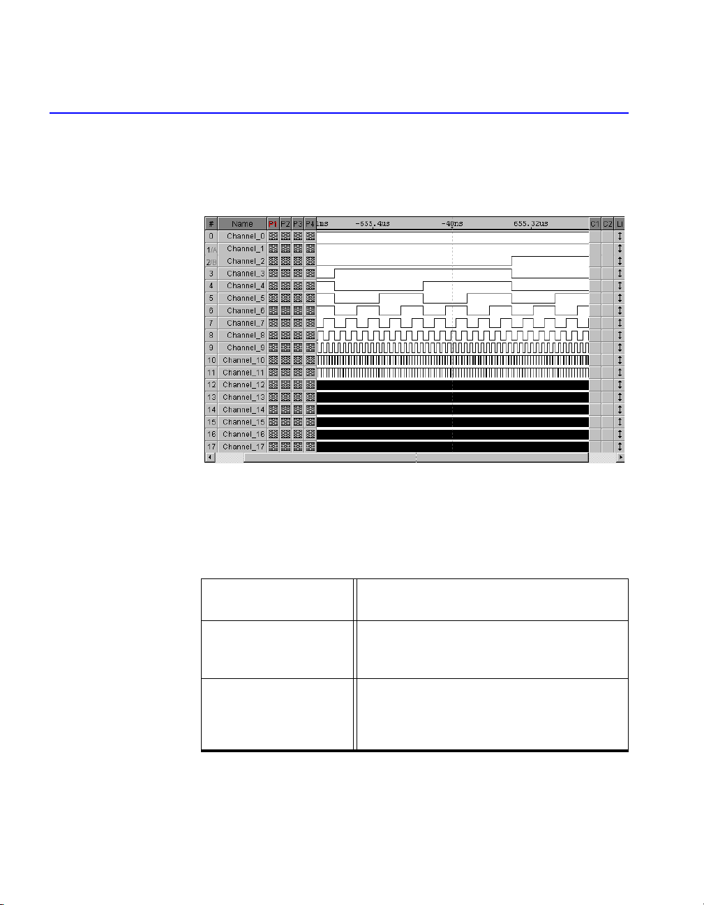
design in the FPGA. The Analyze module is an 18-channel logic
analyzer that automatically displays the signals for both probe outputs
(and up to 16 additional signals) on the target system. You may sample
data asynchronously or synchronously at 100 MHz. Channel 1 and 2 of
the logic analyzer connect to the PRA and PRB signals on the FGPA
automatically. Silicon Explorer II uses the remaining 16 channels of the
logic analyzer to examine other signals on the board.
Actel also offers Silicon Explorer II Lite. SE II Lite enables only the
Command module and relies on an external scope or logic analyzer for
viewing signals.

2
System Requirements
The system requirements for Silicon Explorer II and Silicon Explorer II
Lite are:
• Designer R1-2000 or later
• Pentium-133 or equivalent
•Microsoft
®Windows 95, 98 or NT™4.0
• 8 MB RAM (minimum); 16 MB recommended
Connecting to the PC
Silicon Explorer II and Silicon Explorer II Lite connect to a standard
serial port using an 8250 or 16550 UART. Establish communication via
the 9-Pin D-Sub connector.
Software Settings
Silicon Explorer II sets itself to Demo mode on installation. From the
Device menu, select Silicon Explorer II or Silicon Explorer, depending
on your version of the software. Choose the desired port (COM1
through COM4) from the Port drop-down list in the Device menu. The
software continuously polls the hardware for activity. Setting the port
to the Demo mode prevents the application from opening any COM
ports on your system. The serial port saves information in the
“analyze.ini” file found in your Windows directory. The default data
transfer speed is 115,200 baud. At this speed data transfer for the entire
buffer is less than 15 seconds.
You can download the latest version of the Explorer software from the
Actel website at http://www.actel.com/support/updates or at
http://www.actel.com/custsup/updates/siliexp/index.html
Note: Many notebook computers share the external COM port with a
built-in infrared (IR) port. You may have to enter your CMOS
setup menu to enable the external COM port.

3
1
Connecting Silicon Explorer II
This section describes the procedures required to connect Silicon
Explorer II to your device, powering Silicon Explorer II, SE II
connector types, logic analysis, and the Explore software.
Powering Silicon Explorer II
SE II draws power from the external power supply (provided) or by
connecting the VIO pin to a power source (such as might exist on a
PCB). You must connect VIO to a reference voltage when using the
external power supply. Actel recommends using the external power
supply when the target system cannot supply enough current to run SE
II. See Table 1-1 for a list of possible power configurations.
When you apply power, the yellow “heart beat” LED on Silicon
Explorer II begins to blink.
Actel designed Silicon Explorer II hardware to withstand abuse
normally found in a lab environment. However, long term exposure to
out-of-range conditions can cause failure. In particular, long term
connection to reverse- or over-voltage power conditions can cause
thermal failure.
Table 1-1. Power Configurations for Silicon Explorer II
I/O Power Supply External SE II Power
Supply VIO
2.5V Required 2.5V
3.3V Optionala
a. If your current system is limited, you must use the external power supply
and use VIO as the reference voltage. See Table 1-2 for more information
about SE II current requirements.
3.3V
5.0V Optionala5.0v
Chapter 1: Connecting Silicon Explorer II
4
Current
Consumption
Silicon Explorer II is a CMOS device and exhibits very low current
consumption when idle. Current consumption rises rapidly to several
hundred milliamps during acquisition. If your power supply is unable
to supply the necessary current, SE II or your target may reset.
Table 1-2 is a guide to typical current consumption based on an
acquisition rate at 5V — current will be proportionately higher at 3V.
Connector Types
Silicon Explorer II has a 22-pin (18 channels, a clock, VIO, GND, and
clock GND) and a 16-pin connector for controlling the ActionProbe
circuitry and reading the design checksum. Silicon Explorer II Lite has
only the 16-pin and 26-pin connector (the large 26-pin connector is not
used). Table 1-3 is a summary of the connector pins and their
functions.
Logic Analysis Note: This section does not apply to Silicon Explorer II Lite.
Table 1-2. Typical Current Consumption
Acquisition Rate Current@5V
IDLE 75ma
10 MHz 300ma
20 MHz 400ma
50 MHz 500ma
100 MHz 700ma
Table 1-3. Connector Types
Connector Type Mode
22-pin Logic Analysis
16-pin ActionProbe Control

Connector Types
5
Actel Silicon Explorer II ships with a replaceable target cable assembly
(TCA-8020A) that interfaces Silicon Explorer II with your target system.
To connect Silicon Explorer II, align the short red wire on the TCA-
8020 with the red dot on the case and fully insert the 2mm header. The
contacts on the TCA-8020 accept standard 0.025" round or square test
accessories.
Connect any of Silicon Explorer IIs 18-channel leads to the desired
target signals using standard test accessories. For synchronous
sampling, connect the CLKIN lead to the target clock, which requires a
continuous signal. If the clock is greater than 20 MHz, connect the CLK
GND (twisted pair) to a ground point near the CLK lead.
Probe Leads Connect the probe leads by attaching one of two supplied cable
assemblies.
One 16-pin cable assembly terminates in individual 0.025 connectors
that connect to 0.025 headers or microclips according to the labels on
the wires. The other assembly interfaces directly to the target board
with a 16-pin header when you install the target according to the pin-
out shown in Figure 1-1.
Figure 1-1. Silicon Explorer II Probe Connector Pin-Out
SDI/TDI
DCLK/TCK
SDO/TDO
TMS
PRB
PRA
MODE/CSn
V
IO
GND
GND
GND
2
3 4
1
5 6
7 8
910
11 12
13 14
15 16
COSn
ERRORn
M0
M1
M2

Chapter 1: Connecting Silicon Explorer II
6
Connect the probe leads according to Table 1-4 below.
Connecting Silicon Explorer II
The diagrams below describe, in detail, how to connect the Silicon
Explorer II for the various device families. Figure 1-2 shows how to
connect Silicon Explorer II to the ACT1/A40MX devices, Figure 1-3
Table 1-4. Matching Probe Pins to Device Pins a
a. ERRORn, CONn, M2, M1, M0 pins are not required for use with Silicon
Explorer II.
Probe Act1, 40MX ACT2, 42MX,
3200DX SX/SX-A/eX
Mode Mode Mode Not Used
GNDb
b. You may connect any or all GND pins.
GND GND GND
SDI/TDI SDI SDI TDI
DCLK/TCK DCLK DCLK TCK
SDO/TDO PRA SDO TDO
TMS Not Used Not Used TMS
VIO VCCI VCCI VCCI
PRA PRA PRA PRA
PRB PRB PRB PRB
Connecting Silicon Explorer II
7
shows the setup for ACT2/XL/ACT3/DX and A42MX devices, and
Figure 1-4 shows the correct setup for SX/SX-A and eX devices.
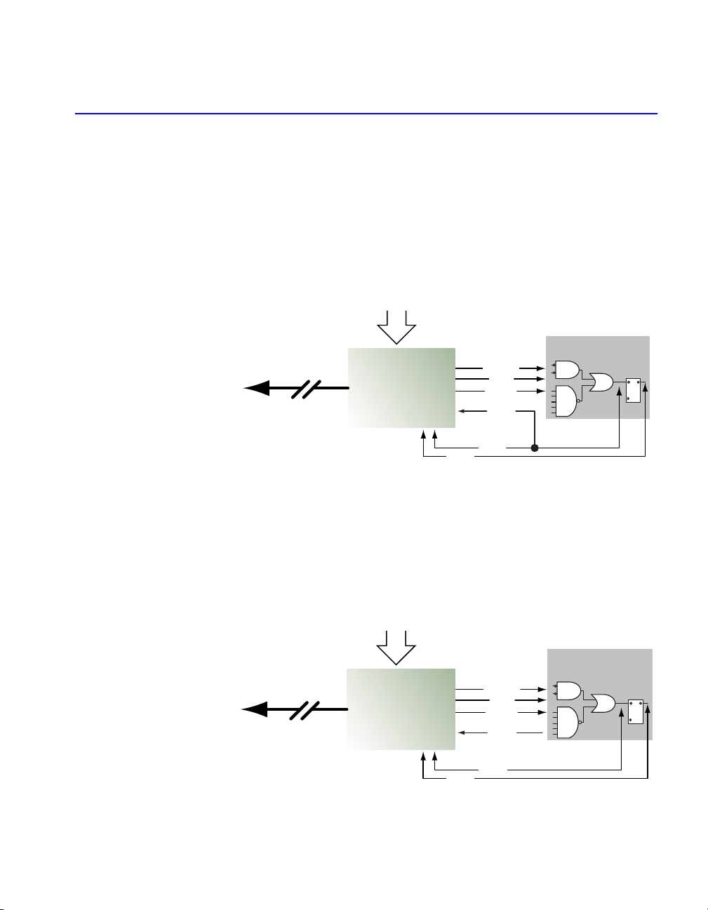
Figure 1-2. ACT1/A40MX Silicon Explorer II Setup
Figure 1-3. ACT2/XL/ACT3/DX/A42MX Silicon Explorer II Setup
ACT1/A40MX
Silicon Explorer Setup
Silicon
Explorer
MODE
SDI
DCLK
SDO
PRA
PRB
Serial Connection
to Windows PC
16 Logic Analyzer Channels
ACT1/A40MX
ACT2/XL/ACT3/DX/A42MX
Silicon Explorer Setup
Silicon
Explorer
MODE
SDI
DCLK
SDO
PRA
PRB
Serial Connection
to Windows PC
16 Logic Analyzer Channels
ACT2/XL/DX/ACT3
A42MX

Chapter 1: Connecting Silicon Explorer II
8
Figure 1-4. SX/SX-A/eX Silicon Explorer II Setup
The probing of an SX-A or eX device may require special setup
because it Actel recommends that you use a series 70 ohm termination
on all the probe connectors (TDI, TDO, TCK, TMS, PRA, PRB). The 70
ohm series termination is used to prevent data transmission corruption
during probing and reading checksum.
SX/SX-A/eX
Silicon Explorer Setup
Silicon
Explorer
TMS
TDI
TCK
TDO
PRA
PRB
Serial Connection
to Windows PC
16 Logic Analyzer Channels
SX/SX-A/eX

9
2
Silicon Explorer Software
The Explorer software consists of two components, the Command
module and the Analyze module. The Command module of the
Explore software lists all the observable nets in the FPGA. Use the
Command module to verify that you programmed the correct design in
the FPGA. The Analyze module is an 18-channel logic analyzer that
automatically displays the signals for both probe outputs (and up to 16
additional signals) on the target system.
Figure 2-1. Silicon Explore Window
Signal Name
Bus Control
Zoom Buttons Trigger Position
Status COM port Silicon Explorer
Status

Chapter 2: Silicon Explorer Software
10
Using the Command Module
The Command module is the interface used to select internal nodes in
the Actel FPGA family. The following sections describe exploring with
the probe.
Figure 2-2. Command Module
Explore the
FPGA
The following procedures describe how to use the Command module
to examine an Actel FPGA.
To open a probe file:
1. Launch Silicon Explorer. Select Silicon Explorer from the
Designer menu under Programs in the Start menu.
2. Select a Probe (.prb) file to open. Select the Open command
from the File menu. Choose (*.prb) as the File type and double-click
Using the Command Module
11
the desired probe file. You may also open a probe file in Silicon
Explorer by double-clicking the “Open Actel Probe File” icon.
Explore uses a .prb file exported from Designer during analysis.
The exported file contains device information, net names, and node
location information. After the .prb file opens, verify the
information displayed in the tree structure in the Analyze window.
To export a probe file from Designer:
1. Launch Designer.
2. Open your design file.
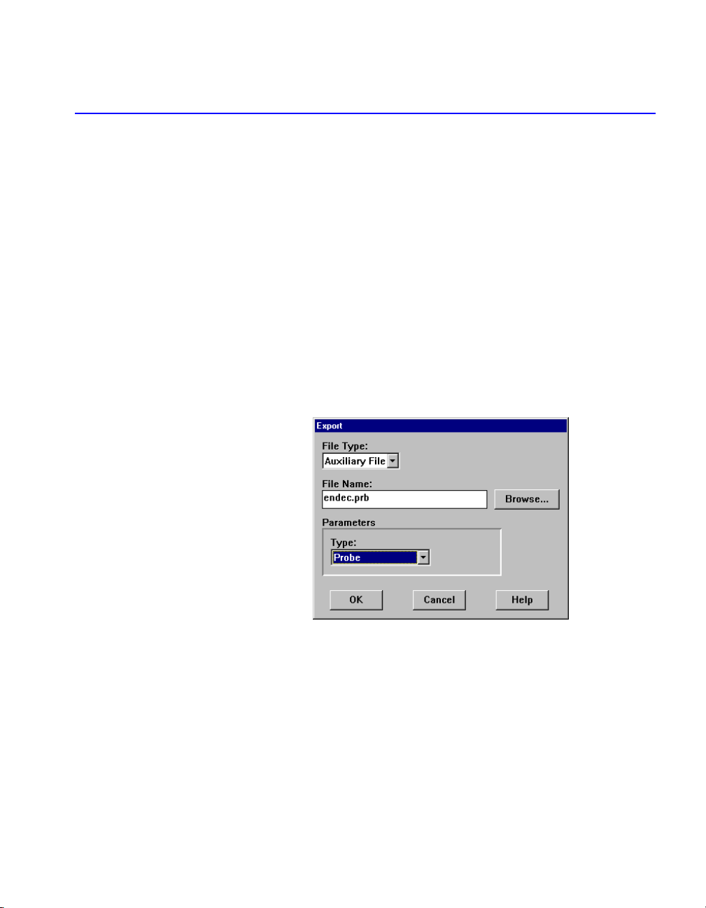
3. Open the Export dialog box. Select Export from the File menu to
view the Export dialog box (Figure 2-3).
Figure 2-3. Designer File Export Dialog Box
4. Select Auxiliary File from the File Type pull-down menu.
5. Select Probe from the Type pull-down menu.
6. Select OK to continue.
To verify the checksum:
First, ensure that that the SDO/TDO is connected. Then click the
Checksum button. Once you open a Probe file and make a device
connection, read the checksum of the target device and compare it to

Chapter 2: Silicon Explorer Software
12
the checksum in the Probe file by double-clicking the Checksum
button. Table 2-1 lists and explains the error messages.
To probe a node:
1. Select the desired signal from the tree by clicking the net
name (see Figure 2-1). You can use the filter box to search nets
quickly. Use multiple wildcard characters (“*”) to restrict your
search.
2. Click the PRA or PRB button. Silicon Explorer II routes the
selected node to the probe pin and switches the corresponding
analyzer input to the probe connector. The Analyze module
displays the net name.
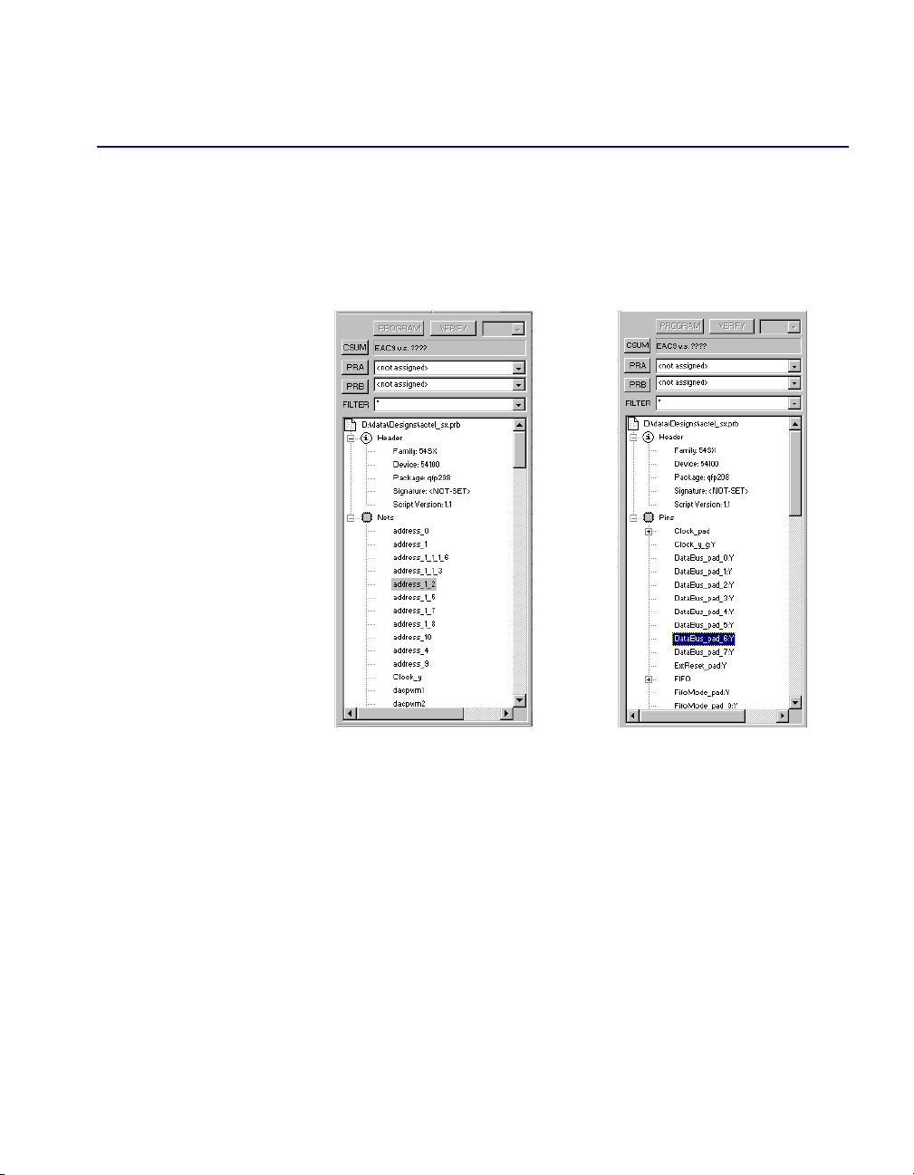
You can modify the tree information to reflect the design’s internal net
names or pin names by right-clicking the Nets icon and selecting either
Table 2-1. Checksum Error Messages
Error Message Explanation
Checksum: 383A vs. ???? Checksum is not readable because the probe
is disconnected or not powered.
Checksum: 383A vs. 0000
The checksum does not match the file.
or
The SDO/TDO probe-side pin is not properly
connected to the device. Please see Table 1-4
on page 6 for the proper connection.
Using the Analyze Module
13
“Show Nets” or “Show Pins”. See Figure 2-4 for examples of the two
types of displays.
Figure 2-4. Command Module Display Styles
If you cannot find a net, it is possible that the net was optimized by
Designer. Refer to “Troubleshooting” on page 27 for more information
about the limitations in probing Actel devices using Silicon Explorer.
Using the Analyze Module
Note: This section does not apply to Silicon Explorer II Lite, since it
does not contain the Analyze module.
Open Silicon Explorer II and check the status in the lower right corner
of the display. If you have properly selected the COM port and
powered up Silicon Explorer II, then the status is IDLE. The Analyze
“Show Nets” Display “Show Pins” Display
Chapter 2: Silicon Explorer Software
14
module captures 64K samples of each channel and uploads them to
the host over the serial port.
Figure 2-5. Analyze Module
Set acquisition parameters from the tool bar or the pull-down menus.
See Table 2-2 for a summary of the parameters.
Once you set the acquisition parameters, click the Run button (red
triangle) to begin acquisition. The analyzer begins capturing data. After
you acquire the initial 64K samples, sampling continues until Silicon
Table 2-2. Acquisition Parameters
Acquisition Speed 10 Khz to 100 MHz asynchronous or
synchronous to 100 MHz
Trigger Position
25% to 75%
50% to 50%
75% to 25%
Trigger Pattern
Click on individual signals in the T column to
specify don’t care, low, high, rising, falling or
either edge. The trigger pattern is the logical
AND of the 18 patterns.
Other manuals for Silicon Explorer II
1
Table of contents


