manuals.online logo
Brands
  1. Home
  2. •
  3. Brands
  4. •
  5. Agilent Technologies
  6. •
  7. Power Supply
  8. •
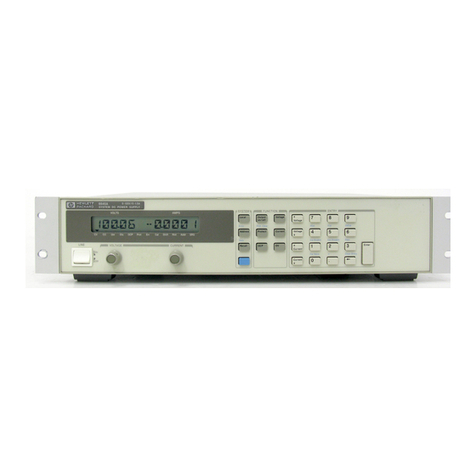
  9. Agilent Technologies 6625A User manual

Agilent Technologies 6625A User manual

(217) 352-9330 | [email protected] | artisantg.com
-~
ARTISAN
®
~I
TECHNOLOGY
GROUP
Your definitive source
for
quality
pre-owned
equipment.
Artisan Technology
Group
Full-service,
independent
repair
center
with
experienced
engineers
and
technicians
on staff.
We
buy
your
excess,
underutilized,
and
idle
equipment
along
with
credit
for
buybacks
and
trade-ins
.
Custom
engineering
so
your
equipment
works
exactly as
you
specify.
•
Critical
and
expedited
services
•
Leasing
/
Rentals/
Demos
• In
stock/
Ready-to-ship
•
!TAR-certified
secure
asset
solutions
Expert
team
ITrust
guarantee
I
100%
satisfaction
All
tr
ademarks,
br
a
nd
names, a
nd
br
a
nd
s a
pp
earing here
in
are
th
e property of
th
e
ir
r
es
pecti
ve
ow
ner
s.
Visit our website - Click HERE
MULTIPLE OUTPUT LINEAR SYSTEM
DC POWER SUPPLY
6628A, and 6629A
* For instruments with higher Serial Numbers, a change page may be included.
5
SERVICE MANUAL
Agilent Part No 06626-90003
AGILENT MODELS 6625A, 6626A,
Microfiche Part No. 06626-90004 Printed in Malaysia: September, 2001
Agilent Model 6625A, Serial 3738A-01389 through 01408
US37380101 and up
Agilent Model 6626A, Serial 3737A-02259 through 02328
US37370101 and up
Agilent Model 6628A, Serial 3738A-00683 through 00727
US37380101 and up
Agilent Model 6629A, Serial 3738A-00968 through 00997
US37380101 and up
Artisan Scientific - Quality Instrumentation ... Guaranteed | (888) 88-SOURCE | www.artisan-scientific.com
CERTIFICATION
Agilent Technologies certifies that this product met its published specifications at time of shipment from the factory. Agilent
Technologies further certifies that its calibration measurements are traceable to the United States National Bureau of
Standards, to the extent allowed by the Bureau’s calibration facility, and to the calibration facilities of other International
Standards Organization members.
WARRANTY
This Agilent Technologies hardware product is warranted against defects in material and workmanship for a period of three
years from date of delivery. Agilent software and firmware products, which are designated by Agilent for use with a
hardware product and when properly installed on that hardware product, are warranted not to fail to execute their
programming instructions due to defects in material and workmanship for a period of 90 days from date of delivery. During
the warranty period Agilent Technologies will, at its option, either repair or replace products which prove to be defective.
Agilent does not warrant that the operation of the software, firmware, or hardware shall be uninterrupted or error free.
For warranty service, with the exception of warranty options, this product must be returned to a service facility designated
by Agilent. Customer shall prepay shipping charges by (and shall pay all duty and taxes) for products returned to Agilent
for warranty service. Except for products returned to Customer from another country, Agilent shall pay for return of
products to Customer.
Warranty services outside the country of initial purchase are included in Agilent’s product price, only if Customer pays
Agilent international prices (defined as destination local currency price, or U.S. or Geneva Export price).
If Agilent is unable, within a reasonable time to repair or replace any product to condition as warranted, the Customer shall
be entitled to a refund of the purchase price upon return of the product to Agilent.
LIMITATION OF WARRANTY
The foregoing warranty shall not apply to defects resulting from improper or inadequate maintenance by the Customer,
Customer-supplied software or interfacing, unauthorized modification or misuse, operation outside of the environmental
specifications for the product, or improper site preparation and maintenance. NO OTHER WARRANTY IS EXPRESSED
OR IMPLIED. Agilent SPECIFICALLY DISCLAIMS THE IMPLIED WARRANTIES OF MERCHANTABILITY AND
FITNESS FOR A PARTICULAR PURPOSE.
EXCLUSIVE REMEDIES
THE REMEDIES PROVIDED HEREIN ARE THE CUSTOMER’S SOLE AND EXCLUSIVE REMEDIES. Agilent
SHALL NOT BE LIABLE FOR ANY DIRECT, INDIRECT, SPECIAL, INCIDENTAL, OR CONSEQUENTIAL
DAMAGES, WHETHER BASED ON CONTRACT, TORT, OR ANY OTHER LEGAL THEORY.
ASSISTANCE
The above statements apply only to the standard product warranty. Warranty options, extended support contracts, product
maintenance agreements and customer assistance agreements are also available. Contact your nearest Agilent
Technologies Sales and Service office for further information on Agilent’s full line of Support Programs.
Artisan Scientific - Quality Instrumentation ... Guaranteed | (888) 88-SOURCE | www.artisan-scientific.com
SAFETY SUMMARY
The following general safety precautions must be observed during all phases of operation, service, and repair of this
instrument. Failure to comply with these precautions or with specific warnings elsewhere in this manual violates safety
standards of design, manufacture, and intended use of the instrument. Agilent Technologies assumes no liability for the
customer’s failure to comply with these requirements.
BEFORE APPLYING POWER.
Verify that the product is set to match the available line voltage and the correct fuse is installed.
GROUND THE INSTRUMENT.
This product is a Safety Class 1 instrument (provided with a protective earth terminal). To minimize shock hazard, the instrument chassis
and cabinet must be connected to an electrical ground. The instrument must be connected to the ac power supply mains through a three-
conductor power cable, with the third wire firmly connected to an electrical ground (safety ground) at the power outlet. For instruments
designed to be hard-wired to the ac power lines (supply mains), connect the protective earth terminal to a protective conductor before any
other connection is made. Any interruption of the protective (grounding) conductor or disconnection of the protective earth terminal will
cause a potential shock hazard that could result in personal injury. If the instrument is to be energized via an external autotransformer for
voltage reduction, be certain that the autotransformer common terminal is connected to the neutral (earthed pole) of the ac power lines
(supply mains).
FUSES.
Only fuses with the required rated current, voltage, and specified type (normal blow, time delay, etc.) should be used. Do not use repaired
fuses or short circuited fuseholders. To do so could cause a shock or fire hazard.
DO NOT OPERATE IN AN EXPLOSIVE ATMOSPHERE.
Do not operate the instrument in the presence of flammable gases or fumes.
KEEP AWAY FROM LIVE CIRCUITS.
Operating personnel must not remove instrument covers. Component replacement and internal adjustments must be made by qualified
service personnel. Do not replace components with power cable connected. Under certain conditions, dangerous voltages may exist even
with the power cable removed. To avoid injuries, always disconnect power, discharge circuits and remove external voltage sources before
touching components.
DO NOT SERVICE OR ADJUST ALONE.
Do not attempt internal service or adjustment unless another person, capable of rendering first aid and resuscitation, is present.
DO NOT EXCEED INPUT RATINGS.
This instrument may be equipped with a line filter to reduce electromagnetic interference and must be connected to a properly grounded
receptacle to minimize electric shock hazard. Operation at line voltages or frequencies in excess of those stated on the data plate may
cause leakage currents in excess of 5.0 mA peak.
SAFETY SYMBOLS.
Instruction manual symbol: the product will be marked with this symbol when it is necessary for the user to refer to the
instruction manual (refer to Table of Contents) .
Indicates hazardous voltages.
Indicate earth (ground) terminal.
The WARNING sign denotes a hazard. It calls attention to a procedure, practice, or the like, which, if not correctly
performed or adhered to, could result in personal injury. Do not proceed beyond a WARNING sign until the
indicated conditions are fully understood and met.
The CAUTION sign denotes a hazard. It calls attention to an operating procedure, or the like, which, if not correctly
performed or adhered to, could result in damage to or destruction of part or all of the product. Do not proceed
beyond a CAUTION sign until the indicated conditions are fully understood and met.
DO NOT SUBSTITUTE PARTS OR MODIFY INSTRUMENT.
Because of the danger of introducing additional hazards, do not install substitute parts or perform any unauthorized modification to the
instrument. Return the instrument to an Agilent Technologies Sales and Service Office for service and repair to ensure that safety features
are maintained.
Instruments which appear damaged or defective should be made inoperative and secured against unintended operation until they can be
repaired by qualified service personnel
Artisan Scientific - Quality Instrumentation ... Guaranteed | (888) 88-SOURCE | www.artisan-scientific.com
SAFETY SUMMARY (continued)
GENERAL
Any LEDs used in this product are Class 1 LEDs as per IEC 825-1.
ENVIRONMENTAL CONDITIONS
This instrument is intended for indoor use in an installation category II, pollution degree 2 environment. It is designed to
operate at a maximum relative humidity of 95% and at altitudes of up to 2000 meters. Refer to the specifications tables for the
ac mains voltage requirements and ambient operating temperature range.
SAFETY SYMBOL DEFINITIONS
Symbol Description Symbol Description
Direct current Terminal for Line conductor on permanently
installed equipment
Alternating current Caution, risk of electric shock
Both direct and alternating current Caution, hot surface
Three-phase alternating current Caution (refer to accompanying documents)
Earth (ground) terminal In position of a bi-stable push control
Protective earth (ground) terminal Out position of a bi-stable push control
Frame or chassis terminal On (supply)
Terminal for Neutral conductor on
permanently installed equipment Off (supply)
Terminal is at earth potential
(Used for measurement and control
circuits designed to be operated with
one terminal at earth potential.)
Standby (supply)
Units with this symbol are not completely
disconnected from ac mains when this switch is
off. To completely disconnect the unit from ac
mains, either disconnect the power cord or have
a qualified electrician install an external switch.
Herstellerbescheinigung
Diese Information steht im Zusammenhang mit den Anforderungen der
Maschinenläminformationsverordnung vom 18 Januar 1991.
* Schalldruckpegel Lp <70 dB(A) * Am Arbeitsplatz * Normaler Betrieb
* Nach EN 27779 (Typprüfung).
Manufacturer’s Declaration
This statement is provided to comply with the requirements of the German Sound Emission Directive,
from 18 January 1991.
* Sound Pressure Lp <70 dB(A) * At Operator Position * Normal Operation
* According to EN 27779 (Type Test).
Edition2September, 2001
© Copyright 2001 Agilent Technologies, Inc.
Artisan Scientific - Quality Instrumentation ... Guaranteed | (888) 88-SOURCE | www.artisan-scientific.com
CONTENTS
Section I
INTRODUCTION
1-1 SCOPE ……………………………………………………1-1
1-2 SAFETY CONSIDERATIONS…………………………..1-1
1-3 INSTRUMENT AND MANUAL
IDENTIFICATION……………………………………….1-1
1-4 FIRMWARE REVISIONS ……………………………….1-1
Section II
PRINCIPLES OF OPERATION
2-1 INTRODUCTION………………………………………..2-1
2-2 OVERALL BLOCK DIAGRAM DESCRIPTION
(Figure 2-1)………………………………………………..2-1
2-3 AC Input Circuits………………………………………..2-1
2-4 GPIB Board.……………………………………………... 2-1
2-5 FrontPanel ……………………………………………….2-1
2-6 Output Boards …………………………………………2-1
2-7 GPIB BOARD (Figure 2-3)……………………………...2-3
2-8 GPIB Interface …………………………………………...2-3
2-9 System MicroComputer…………………………………2-4
2-16Output Boards Interface………………………………...2-4
2-20FrontPanel Interface…………………………………...2-5
2-23BiasSupply and StartUp ……………………………….2-5
2-24OUTPUT BOARD ……………………………………… 2-7
2-25 SecondaryInterfaceCircuits
(Figure 2-4)……………………………………………… 2-7
2-37Powermesh and Control Circuits
(Figure 2-5)…………………………………………… 2-10
Section III
VERIFICATION
3-1 INTRODUCTION………………………………………..3-1
3-2 TEST EQUIPMENT REQUIRED ………………………3-1
3-3 OPERATION VERIFICATION TESTS ………………. 3-1
3-4 PERFORMANCE TESTS ………………………………..3-1
3-5 Introduction………………………………………………3-1
3-6 Measurement Techniques ………………………………3-1
3-10Constant Voltage (CV) Tests……………………………3-4
3-19Constant Current (CC) Tests…………………………..3-10
3-27EXTENDTED TESTS…………………………………...3-13
3-28Output Drift Tests ……………………………………...3-13
Section IV
TROUBLESHOOTING
4-1 INTRODUCTION………………………………………..4-1
4-2 ELECTROSTATIC PROTECTION……………………..4-1
4-3 REMOVAL AND REPLACEMENT …………………...4-2
4-4 Top Cover Removal…………………………………….4-2
4-5 Gaining Access to Assemblies in the Supply …………4-2
4-6 GPIB Board Removal..………………………………….4-2
4-8 DUSTCOVERS …………………………………………..4-4
4-9 Replacing the Power Module U338……………………4-4
4-10FrontPanel Removal…………………………………….4-4
4-11Chassis Mounted Components………………………...4-5
4-12TEST EQUIPMENT REQUIRED……………………….4-5
4-13FUSE REPLACEMENT………………………………….4-5
4-14INITIAL TROUBLESHOOTINGAND BOARD
ISOLATION PROCEDURES ..…………………………4-8
4-15 Power-On Self Test………………………………………4-8
4-16 Connector P201 Jumper Positions……………………...4-9
4-17 ERROR Codes and Messages…………………………...4-9
4-18GPIB BOARD AND FRONT PANEL
TROUBLESHOOTING PROCEDURES ……………...4-13
4-19 Test Setup ……………………………………………….4-13
4-20 Post Repair Calibration………………………………...4-13
4-21 Setting the Model Number
(MODEL Command)…………………………………...4-13
4-22 Signature Analysis Testing …………………………4-14
4-23 Test Setup for S.A.……………………………………...4-14
4-24 Firmware Revisions (ROM? Command)……………..4-14
4-25 OUTPUT BOARD TROUBLESHOOTING
PROCEDURES ………………………………………….4-30
4-26 Test Setup ……………………………………………….4-30
4-27 Post Repair Calibration ………………………………..4-30
4-28 Self Exercise Routine on the Output Board ………….4-30
4-29 Troubleshooting Analog Multiplexer U323 and
Readback Using VMUX? Command …………………4-49
4-30 Understanding and Troubleshooting the Signal
Processor (U327)………………………………………...4-50
4-33 Power Module Signals…………………………………4-54
4-34 Miscellaneous Trouble Symptoms and Remedies ….4-54
Section V
REPLACEABLE PARTS
5-1 INTRODUCTION………………………………………..5-1
5-2 HOW TO ORDER PARTS………………………………5-1
i
Artisan Scientific - Quality Instrumentation ... Guaranteed | (888) 88-SOURCE | www.artisan-scientific.com
CONTENTS (Cont. )
Section VI
CIRCUIT DIAGRAMS
6-1 INTRODUCTION………………………………………..6-1
6-2 FUNCTIONAL SCHEMATIC DIAGRAMS …………..6-1
6-3 COMPONENT LOCATION ILLUSTRATIONS ……...6-1
Appendix A
LOGIC SYMBOLOGY
ii
Artisan Scientific - Quality Instrumentation ... Guaranteed | (888) 88-SOURCE | www.artisan-scientific.com
iii
LIST OF FIGURES
Figure Page
2-1 Agilent 6625A, 6826A, 6628A and 6629A Multiple Output Power Supplies, Block Diagram ……………………………...2-2
2-2 Output Operating Ranges for Agilent Models 6625A, 6626A, 6628A and 6629A …………………………………………2-3
2-2 HP-IB Board, Block Diagram ……………………………………………………………………………………………………..2-6
2-4 Output Board, Secondary Interface Circuits, Block Diagram ………………………………………………………………….2-9
2-5 Output Board, Power Mesh and Control Circuits, Block …………………………………………………………………….2-12
2-6 Voltage and Current Control Circuits, Simplified Schematic ………………………………………………………………..2-13
2-7 Typical Output Range Characteristics ………………………………………………………………………………………….2-14
2-8 Typical Downprogramming Characteristics Below 2.0 V …………………………………………………………………….2-16
2-9 Overvoltage Protection Circuits, Block Diagram ……………………………………………………………………………...2-17
3-1 Operating Ranges Available in Models 6625A, 6626A, 6820A and 6629A …………………………………………………..3-3
3-2 Current Monitoring Resistor Setup ………………………………………………………………………………………………3-4
3-3 Basic Test Setup …………………………………………………………………………………………………………………….3-5
3-4 Transient Recovery Time Test Setup …………………………………………………………………………………………….3-6
3-5 Transient Response Waveform. …………………………………………………………………………………………………..3-7
3-6 Negative Current Limit (- CC) Readback Accuracy ……………………………………………………………………………3-9
3-7 Down Programming Speed Test Setup ………………………………………………………………………………………3-12
3-8 CV Down Programming Speed Test Waveform ………………………………………………………………………………3-13
3-9 CV Up Programming Speed Test Setup ………………………………………………………………………………………..3-13
3-10 CV Up Programming Test Waveform ………………………………………………………………………………………….3-14
3-11 Fixed OV Protection Test Setup …………………………………………………………………………………………………3-14
3-I2 OV External Trip Test Connection ……………………………………………………………………………………………3-14
4-1 Agilent 6625A, 6626A, 6628A and 6629A Multiple Output Supplies, Assembly Locations ……………………………….4-3
4-2 HP-IB, Board, Fuse and Test Point Locations …………………………………………………………………………………...4-6
4-3 Output Board 1 and 2 Fuse and Test Point Locations ………………………………………………………………………….4-7
4-4 Output Board 3 and 4 Fuse and Test Point Locations ………………………………………………………………………….4-9
4-5 Initial Troubleshooting and Board Isolation …………………………………………………………………………………..4-13
4-6 HP-IB Board and Front Panel Troubleshooting ……………………………………………………………………………….4-15
4-7 Signature Analysis Test Setup ………………………………………………………………………………………………….4-17
4-8 Output Board Troubleshooting …………………………………………………………………………………………………4-29
4-9 Output Board Waveform During Self Exercise Routine ……………………………………………………………………4-35
4-10 DAC/Amplifier Circuit Troubleshooting ……………………………………………………………………………………...4-36
4-11 Overvoltage Troubleshooting …………………………………………………………………………………………………4-37
4-12 Output Held Low Troubleshooting……………………………………………………………………………………………..4-39
4-13 Output Held High Troubleshooting…………………………………………………………………………………………….4-42
4-14 OV Circuit Will Not Trip Troubleshooting……………………………………………………………………………………..4-43
4-15 Signal Processor U327, Overvoltage Circuit, Simplified Schematic …………………………………………………………4-46
4-16 Signal processor U327, Power-On/Start-Up Circuit, Simplified Schematic ………………………………………………4-46
4-17 Signal processor U327, Status Monitor Circuit, Simplified Schematic ………………………………………………………4-52
4-18 Status Problems Troubleshooting ……………………………………………………………………………………………….4-53
6-1 Power Distribution Schematic….…………………………………………………………………………………………………6-3
6-2 GPIB Board, ComponentLocation ……………………………………………………………………………………………….6-5
6-2 GPIB Board, Schematic Diagram ...……………………………………………………………………………………………….6-6
6-3 Output 1& 2 Board,ComponentLocation..…………………………………………………………………………………..…6-7
6-3 Output 1&2Board,SchematicDiagram.....…………………………………………………………………………………..…6-8
6-4 Output 3& 4 Board,ComponentLocation ..……………………………………….…………………………………………..6-13
6-4 Output 3& 4 Board,Schematic Diagram.………………………………………….…………………………………………..6-14
Artisan Scientific - Quality Instrumentation ... Guaranteed | (888) 88-SOURCE | www.artisan-scientific.com
LIST OF TABLES
Table Page
3-1 Test Equipment Required for Verification ………………………………………………………………………………………… 3-2
3-2 Low Range Voltage and Current Values …………………………………………………………………………………………… 3-4
3-3 Performance Test Record for Agilent 6625A and 6628A ...………………………………………………………………………. 3-15
3-4 Performance Test Record for Agilent 6626A and 6629A ………………………………………………………………………… 3-16
4-1 Test Equipment Required for Troubleshooting …………………………………………………………………………………… 4-5
4-2 Fuses …………………………………………………………………………………………………………………………………….4-6
4-3 Tests Performed at Power-On ..……………………………………………………………………………………………………… 4-8
4-4 Power-On Self Test Error Message ………………………………………………………………………………………………….. 4-9
4-5 ERROR Codes and Messages.………………………………………………………………………………………………………. 4-10
4-6
4-8 GPIB Board S.A. Test No. 3………………………………………………………………………………………………………… 4-20
4-9 GPIB Board S.A. Test No. 4………………………………………………………………………………………………………… 4-21
4-10GPIB Board S.A. Test No. 5………………………………………………………………………………………………………… 4-22
4-11GPIB Board S.A. Test No. 6………………………………………………………………………………………………………… 4-23
4-12GPIB Board S.A. Test No. 7………………………………………………………………………………………………………… 4-24
4-13GPIB Board S.A. Test No. 8………………………………………………………………………………………………………… 4-25
4-14Keyboard SignalPaths………………………………………………………………………………………………………………. 4-27
4-15Microcomputer (U312) Signal Measurements During theSelf Exercise Routine …………………………………………… 4-44
4-16U368 Signal Levels…………………………………………………………………………………………………………………… 4-45
4-17SignalProcessor (U327) SignalLevels …………………………………………………………………………………………….. 4-47
4-18Typical Power Module Voltage Levels ……………………………………………………………………………………………. 4-49
4-19Miscellaneous Trouble Symptoms …………………………………………………………………………………………………. 4-50
5-1 Output Board Configurations ……………………………………………………………………………………………………….. 5-1
5-2 Reference Designators………………………………………………………………………………………………………………… 5-1
5-3 Abbreviations …………………………………………………………………………………………………………………………...5-2
5-4 Federal Manufacturer Codes………………………………………………………………………………………………………… 5-3
5-5 Chassis Parts…………………………………………………………………………………………………………………………… 5-4
5-6 Output Board Replacement Part List…………………………………………………………………………………………………5-7
5-7 25W/.5AReplacement Parts List ……………………………………………………………………………………………………. 5-9
5-8 50W/2A Replacement Parts List …………………………………………………………………………………………………… 5-18
iv
GPIB Board S.A. Test No. 1………………………………………………………………………………………………………… 4-18
4-7 GPIB Board S.A. Test No. 2………………………………………………………………………………………………………… 4-19
Artisan Scientific - Quality Instrumentation ... Guaranteed | (888) 88-SOURCE | www.artisan-scientific.com
Section I
1-1 SCOPE
Wherever applicable, the service instructions given in this
manual refer to pertinent information provided in the
Operating Manual. The information in each manual covers
model 6625A, 6626A, 6628A, and 6629A. The main
differences between the models are the number and type of
outputs each model contains. These differences are specified
in each of the manuals.
The following is a listing of the information contained in this
manual with a brief description concerning its scope and
purpose.
Principles of Operation: Section II provides block diagram
level descriptions of the supply’s circuits. The GPIB
interface (digital circuits), the power control (analog and
digital circuits), and power output (analog circuits) are
described. These descriptions are intended as an aid in
troubleshooting.
Verification: Section III contains test procedures that check
the operation of the supply to ensure that it meets the
specifications given in Section I of the Operating manual.
Troubleshooting: Section IV contains board level
troubleshooting procedures to isolate a malfunction to a
defective board (GPIB or output board) or assembly (front
panel, power transformer, or cable assembly). Additional
troubleshooting procedures are provided to isolate the fault
to a defective component on the board. Board and assembly
level removal and replacement procedures are also given in
this section.
NOTE
Calibration is generally required after a repair is made.
Software calibration procedures are given in Appendix A
of the Operating Manual. After calibration is completed,
perform the applicable test(s) given in Section III of this
manual to ensure that the supply meets all specifications.
Replaceable Parts: Section V provides a listing of
replaceable parts for all electronic components and
mechanical assemblies.
Circuit Diagrams: Section VI contains functional schematics
on the functional schematics also appear on the block
diagrams in Section II. Thus, the descriptions in Section II
can be correlated with both the block diagrams and the
schematics.
Logic Symbology: Appendix A gives a brief description of
the logic symbols used on the functional schematics.
Fault Indicator (FLT) and Remote Inhibit (INH): A fault
indicator and remote inhibit circuit, which provide
additionalshutdownprotection should eitherthe GPIB
and/or controller fail, are available optionally. See a
separate document entitled, "Appendix E Option 750
Operating Instructions" for the Multiple Output Linear
System DC Power Supply Agilent Models 662xA (Agilent
P/N 5957-6372).
1-2 SAFETY CONSIDERATIONS
This product is a Safety Class 1 instrument, which means
that it is provided with a protective earth terminal. The
instrument and this manual should be reviewed for safety
markings and instructions before operation. Refer to the
Safety Summary page at the beginning of this manual for a
summary of general safety information. Safety information
for specific procedures is located at appropriate places in the
manual.
1-3 INSTRUMENT AND MANUAL
IDENTIFICATION
Agilent Techonologies instruments are identified by a two-
part Serial number, i.e. 2601A-00101. The first part of the
serial number (the prefix) is a number/letter combination
that denotes either the date of manufacture or the date of a
significant design change. It also indicates the country of
manufacture. The first two digits indicate the year (25 =
1985, 26 = 1986, etc), the second two digits indicate the week,
and “A” designates the U.S.A. The second part of the serial
number is a different sequential number assigned to each
instrument.
and component location diagrams. The names that appear
INTRODUCTION
1-1
This manual contains principles of operation, verification,
and troubleshooting information for the power supply.
Replaceable parts lists and circuit diagrams are also
provided. Installation, operation, programming, and
calibration procedures as well as detailed specifications are
given in a separate Operating Manual, Agilent Part No.
06626-90001.
Artisan Scientific - Quality Instrumentation ... Guaranteed | (888) 88-SOURCE | www.artisan-scientific.com
If the serial number prefix on your power supply differs
from that shown on the title page of this manual, a yellow
Manual Change sheet that is supplied with the manual
add/or manual backdating changes in Appendix A of this
manual define the differences between your supply and the
supply described in this manual. The yellow change sheet
may also contain information for correcting errors in the
manual.
The serial number prefixes listed on the front of this manual
indicate the versions of the supplies that were available
when the manual was issued. If the serial prefix of your
supply is not listed in this manual, the manual may include
a yellow “Manual Changes” sheet. That sheet updates this
manual by defining any differences between the version of
your supply and the versions included here, and may also
include information for correcting any manual errors. Note
that because not all changes to the product require changes
to the manual, there may be no update information required
for your version of the supply.
1-4 FIRMWARE REVISIONS
The Read Only Memory (ROM) chip inside of your supply is
identified with a label that specifies the revision of the
supply’s firmware, see paragraph 4-24
1-2
Artisan Scientific - Quality Instrumentation ... Guaranteed | (888) 88-SOURCE | www.artisan-scientific.com
SectionII
PRINCIPLES OF OPERATION
2-1 INTRODUCTION
The following paragraphs provide block diagram level
descriptions of the power supplies. Differences between the
models are given as required. The descriptions provide a
basic understanding of circuit operation and are intended as
an aid in troubleshooting . It is assumed in the following
discussions that you are familiar with the operating and
programming instructions presented in the Operating
Manual (Agilent Part No. 06626-90001).
2-2 OVERALL BLOCK DIAGRAM DESCRIPTION
(FIGURE 2-1)
Figure 2-1 is a block diagram that illustrates the major
assemblies contained within the power supply. As shown in
the figure, each supply includes acinput circuits, anGPIB
board, front panel display and keyboard, and two or more
output boards.
2-3 AC Input Circuit
2-4 GPIB Board
The GPIB board contains the GPIB interface, system
microcomputer, output boards interface, and front panel
interface. These circuits provide the interface between the
user and the multiple outputs of the power supply. Each
output board is actually an output channel that can be
individuallyselected and controlled over the GPIB or from
thesupply’sfront panel.TheGPIBboardinterprets
commands from the GPIB or from the front panel to
control the selected output. The GPIB boardalso processes
boards. This data may be read back to the controller over
the GPIB and/or displayedon the supply’s front panel.
Also, each output board can be individually calibrated over
the GPIBusing calibration commands (See Appendix A in
Operating Manual). Correction factors are calculated during
calibration and stored in non-volatile memory onthe GPIB
board. The GPIB board is described in greater detail in
paragraph 2-7.
2-5 Front Panel
Most of the remote operations that can be performed via the
GPIB canalso be performed from the supply’s frontpanel.
In addition to the ON/OFF switch already mentioned, the
front panel contains an LCD display and a keypad. The LCD
display consists of an alphanumeric display and status
annunciators. The LCD normally displays the measured
output voltage and current of the selected output. When
programming an output from the front panel keypad, the
selected output channel, the function being programmed,
and the present value will be displayed. The annunciators
indicatewhich outputchannel has been selected and give
GPIB and power supply status information. The keypad
allows control of the supply’s system functions as well as
individual control of each output channel. Detailed
instructions on using the front panel’s display and keypad
are given in the Operating Manual.
2-6 Output Boards
The Agilent 6625A and 6628A contain two output boards
and the Agilent 6626A and 6629A contain four output
boards. The output combinations that correspond to each
model are shown in Figure 2-1. Each isolated output can
supply power in two ranges as shown in Figure 2-2. This
flexibility allows you to use the same output to power loads
with different voltage and current requirements. The output
ranges and operating characteristics of each output are
described in greater detail in Section IV of the Operating
Manual.
As shown in Figure 2-1, each output board contains a
rectifier/filter, power module, control circuit, secondary
interface circuit, and bias supplies.
The ac input to each output board is rectified, filtered, and
applied to the power module regulator. Each output board
employs series regulation techniques. The regulator element
is connected in series with the load and operates in the linear
region (between saturation and cutoff) of the transistor
characteristic curve. Regulation is achieved by varying the
conduction of the series element in response to changes in
the line voltage or the load. The constant voltage CV control
circuit compares the voltage at the output with a reference
voltage and generates a control signal which varies the
conduction of the series regulator to raise or lower the
output voltage as required. The constant current CC control
measurement and status data received from the output
2-1
The ac input circuit consists of a line module on the rear
panel of supply, front panel ON/OFF switch S1, power
transformer (T1), located in the front of the chassis, and a
cooling fan located in the rear of the chassis. The line module
contains a voltage selector card that selects the applicable ac
input voltage: 100 Vac, 120 Vac, 220 Vac, or 240 Vac. The
voltage card selection must match the nominal line voltage
that is connected to the unit. The line module also contains
the main fuse F1. An 8 A fuse (normal blow) must be
installed for a 100/120 VAC input; a4 fuse (normal blow)
must be installed for a 220/240 VAC input. The ac input is
applied to the power transformer when S1 is ON.
Depending on the line module setting, the 120 Vac cooling
fan either runs directly from the line module setting, the 120
VAC cooling fan either runs directly from the line or from
the appropriate transformer tap. The power transformer
provides the main ac inputs to the output boards and also
provides the ac inputs for the bias voltage supplies located
on the GPIB board and eachoutputboard. Acpower
distribution is shown in detail in Figure 6-1 in the rear of this
manual.
Artisan Scientific - Quality Instrumentation ... Guaranteed | (888) 88-SOURCE | www.artisan-scientific.com
2-2
Artisan Scientific - Quality Instrumentation ... Guaranteed | (888) 88-SOURCE | www.artisan-scientific.com
Circuitcompares the voltage at the current monitor resistor
with areferenceandlikewisevariestheconductionofthe
series regulator.
Theinterfacecircuit ontheoutput boardreceivesdigital
signals fromthe GPIBboard and convertsthemtoanalog
signals (reference voltages) which aresent tothe control
circuit to program theoutput voltageandcurrent.
The output boards can be commanded to send measurement
andstatus data back to theGPIBcontrollerand/orto the
displayonthefront panel.Thedata issent back viathe
secondary interfacecircuitand the appropriatecircuitson
the GPIB board.
The outputboard is able tosink current as well as source
current. Current sink limits are fixed at values slightly
higherthanthe maximum currentsource limitfor the
particular outputvoltage operating point.SeeFigure2-7 for
typicalcurrentsource andsinkcharacteristics.The output
board circuits are described in greater in paragraph 2-24.
2-7 GPIB BOARD (FIGURE 2-3)
Figure 2-3 illustrates the major circuits and signalflow on
theGPIBboard.Complete circuit detailsareshownonthe
functionalschematic in therear ofthismanual.
The functional names on the block diagram correspond with
thoseontheschematic sothatthediagrams canbe
correlated. Asshown in Figure2-3, the major circuitsconsist
of the GPIB interface, the system micro-computer, the
output boardsinterface,andthefront panelinterfacecircuit.
2-8 GPIB Interface
These circuits consist of theGPIB bus connector (J201),
transceivers (U203) for the 8 datalinesand 8 control lines,
and the GPIB talker/listener chip (U202). All GPIB (IEEE-
488) functionsareimplementedby theGPIBchipwhich
handlesdata transferbetweenthemicroprocessorandthe
GPIB, handshake protocol, and talker/listener addressing
procedures. The GPIB talker/listener chip is connected to
thedata bus and appears asmemorylocationsto the
microprocessor.
The eight datalines(DIO1-DIO8) of theGPIB are reserved
forthetransferofdata andothermessagesina byte serial,
bitparallel manner. Dataand message transfer is
asynchronous, coordinated bythe three handshakelines
(DAV, NRFD, and NDAC).The power supply canbe atalker
or a listener on theGPIB. The controller dictates the role of
anGPIBdevice by settingtheATN (attention)linetrue and
sending talk or listen addresses on the datalines (DIO1-
DIO8). The powersupply’s GPIB address is stored in the
EEPROM (electrically erasable programmable memory) chip
along withother system variables. You can find outyour
supply’s GPIB address byusing the front panel ADDR key
as described in the operating manual. Asshipped fromthe
factory, the power supply’s address is set to5. Any address
from0 through 30 is a valid address.
There are five GPIB control lines: ATN,IFC, REN,SRQ, and
EOI (IEEE-488). When the controller sets the ATNline true,
all devices on the bus must “listen” to the addresses and
universal commands placed on the bus. When ATN is false,
only devices that are addressed will actively send or receive
data. All unaddressed devices will ignore the data lines
when ATN is false.
2-3
Artisan Scientific - Quality Instrumentation ... Guaranteed | (888) 88-SOURCE | www.artisan-scientific.com
2-9 System Micro-Computer
The system micro-computer decodes and executes all
instructions, and controls all datatransfers. Itconsistsof a
microprocessor, an address decoder, RAM and ROM
memories, databuffers/latches, and a real timeclock as
shown in Figure 2-3.
2-10 Microprocessor and Clock Circuits. These circuits
contain a high performance 8-bitmicroprocessor(U201) and
associated clock circuits.The microprocessoroperates on a1
MHz cycle,whichit derives froma 4 MHz ceramicresonator
oscillator(Y201). The 1MHz Q signal is generated by the
microprocessor for use by other circuit.
A4 millisecond (approximately) clock signal, applied tothe
microprocessorinterrupt input, enablesthemicroprocessor
to keeptrackofrealtime.This allows themicroprocessorto
form necessary tasks on a regular basis. The real timeclock
signalis alsousedto keeptrack ofthetime that haselapsed
since the outputwas last changed. This enables
microprocessor todetermine if a CV/CCmode change
occurred before the selected time delay(see Reprogramming
Delay discussionin Section V of the Operating Manual). The
microprocessorinhibits theOCP functionuntilthedelay is
over.
The microprocessor also uses the 4 millisecond clock to
determinewhento refreshthefront paneldisplay andto
perform other regularly scheduled jobs.
The R/W (read/write) output from the microprocessor
indicatesthedirectionofflowonthedata bus,eitherto or
from the microprocessor. A low level R/W signal indicates
that themicroprocessoriswritingdata onto thedata bus.A
high level R/W signal indicates that the microprocessor is
readingdata that wasplacedonthebus by theaddressed
circuit. The microprocessoruses the addressdecodercircuit
andtheaddressbus to specifythedata transferlocations.
Addresses are valid on the rising edge of the Q signal.
2-11 Data Bus latches (U217) and Buffers(U216). The
timingsequence ofthemicroprocessor issuch thatthe
circuits providingdata for themicroprocessorarede-
selected (address disappears) before the microprocessor can
read the data. The databus latches (U217) latch the datato
be readbythe microprocessor.The datais updated on every
falling Q pulse. Dataputon the databus bythe
microprocessor goesaroundthelatchesthoughbuffers
(U216).
2-12 Free-Run and SignatureAnalysis Jumpers. The data
bus isconnected to the microprocessorthroughajumper
pack (W202). For somesignature analysis tests of the
microprocessor kernel (microprocessor, RAM, ROM), the
databusisbrokenbymovingW202fromtheNORMAL
positionto theNOP position(seeparagraph4-23).This
connects a NOP(no operation) code (free run) tothe
microprocessordata inputs.The NOP codedoes not contain
an address for the next instruction so the microprocessor
goes tothe next highest address. Therefore, the address bus
looks like a 16-bitcounter thatcontinuously rolls overand
startsat zero. The contentsofeach address appear
sequentiallyonthedatabus(othersideofthebreak)In
addition,forallsignatureanalysistests,jumperW201
mustbe movedfromtheNORM RUN positionto theSIG
ANALYSISposition (seeparagraph4-23).
2-13 Address Bus and Address Decoder. The
microprocessor has 16 address lines(A0-A15) allowing it to
address 65,536 locations. The address decoder (U208) allows
each addressablecircuittolookat a shorter address.The
chip select signals (CS0-CS8) are decoded from the higher
order address lines (A12-A15). When a databuffer’s CS is
decoded, it places itsdataon the databus lines. When adata
latch’s CS is decoded, the outputof eachlatch will beset to
the logic state thatis present onthe associated databus line.
If the chip select for the RAM (random accessmemory),
ROM (read only memory),or talker/listener chip is
decoded, the selected circuit will decode the lower order
address bits supplied toit onthe address bus.
2-14 Memory(ROMand RAM). The system microcomputer
contains both ROM(U206) and RAM(U207) devices. The
32KKnon-volatile ROM contains the operating program and
parameters. The 2 K static RAMstoresvariables voltageto
beprogrammed, outputcurrent readback, etc. A third
memorychip,shownin theoutput boardinterfaceblockof
Figure 2-3, is the EEPROM (electrically erasable
programmable memory).The EEPROM(U230) storesall of
thesystemconstants includingcalibrationconstants,the
supply’s GPIB address,and model number (see paragraph
2-19).
2-15 Real Time Clock. The real timeclock (U209) consists
ofa14-stageripplecounterthat dividesthe1MHzQclock
signalfrom the microprocessor to produce a pulse every 4
milliseconds. The real-time clock is used bythe
microprocessor toschedule regular jobs as described
previously.TheTIMER ENABLEsignalresets thecounterto
zero.
2-16 OutputBoardsInterface
2-17 Data Buffers. These3-statebuffers (U212) placethe
serialdata fromeach output board andtheEEPROMonthe
supply’s system microcomputer databus lines whenchip
selectCS3 is decoded. Serial datafrom outputboards 1-4
appears ondatabus lines D0-D3, respectively, and EEPROM
2-4
_
__
__
__
___
___
___________
___
This circuit provides the interface between the system
microcomputer and each of the output boards (up to 4) in
thepowersupply.Data istransferredseriallyonebit at a
time betweenlatches/buffersontheGPIBboardand
optoisolators on the output boards. As shown in Figure 2-3,
the latches/buffers use data bus lines D0-D3 to send/receive
data from the applicable output. Data line D0 is used for
output board 1, D1 for output board 2, D2 for output board
3 (if present), and D3 for output board 4 (if present). A
controlled and regulated 5 volt line is also generated on the
GPIBboardto operate artoftheopto-isolatorsonthe
output boards. In addition to interfacing with the output
boards, the latches/buffers interface with the 4 K bit serial
EEPROM in which system constants are stored.
Artisan Scientific - Quality Instrumentation ... Guaranteed | (888) 88-SOURCE | www.artisan-scientific.com
impedance state when CS3 is not decoded.
2-18 Data Latches. Thesestages(U213) are edge-triggered
D-typeflip-flops.OntherisingedgeoftheCS2chipselect,
the outputof eachstage will beset tothe logic state that is
present on the associated databus line. Databus line D0-D3
are the serial datainputlinesfor outputboards 1-4,
respectively. Databus line D4 controls the TIMER ENABLE
signallineto therealtime clock circuit; D5isthechipselect
linefortheEEPROM;D6istheclocksignalforthe
EEPROM; and D7 is the datainputline for the EEPROM.
Thedata that istransferredbetweentheGPIBboardand
theoutput boards(upto 4)passes through opticalisolators
located on each output board.
2-19 EEPROM.This 4Kbit serial EEPROM (electrically
erasable programmable memory) stores the power supply’s
GPIB address and model number as well as the constants
used in calibratingthe supply. The EEPROM (U230) is
nonvolatile allowing it toretain the stored information after
poweriscycled off andon.
Because the RAM operates faster thanthe EEPROM, at
poweron,thestoreddata isreadinto RAM inthesystem
microcomputer via databus line D7.
The EEPROM’s 4096bits of read/writememory are divided
into 2 pagesof 8X256 each. Each register can be serially
readfromorwrittento using data bus lineD7.Input data is
receivedviaa data latch andoutput data issent viaadata
buffer.
Datawritten tothe EEPROM is stored in a location until it is
updated bya write cycle. The CHIPSELECT and CLOCK
signals are use by the microprocessor tocontrol the
EEPROM’s programmingmodes.AT poweron,the
EEPROM signal holds the EEPROM’s CLOCKsignal off to
protectagainst accidental datawrites when power is initially
applied.
2-20Front PanelInterface
These circuitsprovide theinterface between the supply’s
system microcomputer and the front panes (keyboard and
LCDdisplay).Themicroprocessorusesthedata latches
(U210 ) and databuffers (U214) totransfer databetween the
supply’s system microcomputer and the front panel.
2-21 Data Latches. On the rising edge of the CS5chip select
these D-type flip-flops will beset tothe logic states that are
present onthedata bus lines.
Data bus lineD0-D2arefed to the3to 8linekeyboard
decoder (U211). The microprocessor successively drives
each of the eight open collector outputs of the decoder and
monitorsthefour readback linesfromthekeyboardto
determine which key was pressed. The readback lines are
held high until a depressed key pulls the line low.
2-22 DataBuffers. These 3-state buffers place the keyboard
readbackdataondatabuslinesD4-D7whenchipselectCS4
is decoded. Asstated above, the microprocessor will use this
information todetermine which key was pressed. In
addition buffersprovidethefollowing data onbus lines D0-
D3 when CS4 is decoded:
D0-Alogic 1 (JumperW201 is notinstalled in the
Skip Self Test position) –tells the
microprocessor toperform the self test at
power on;
or
a logic 0 (Jumper W201is installed in the Skip
Self Test position) – tells the microprocessor
not to perform self test at power on.
D1-Alogic 1 (JumperW201 is notinstalled in the
CalLockout position)– tellsthe
microprocessor torespond tocalibration
commands;
or
a logic 0 (Jumper W201 is installed in the Cal
Lockout position)–tellsthemicroprocessor
toignore calibration commands. This jumper
providessecurity against unauthorized
calibration.
D2-A logic 0 indicatesRemote Inhibit istrue
(OPTION750).
D3 - Alogic 1 indicates OPTION 750is installed in
powersupply.
All buffer outputs are held in the high impedance state
disconnecting it from the databus when CS4is not decoded.
2-23BiasSupplyand Start-Up Circuit
The bias supply (U218) provides+5 V bias power tooperate
the circuitson the GPIB board. The start-upcircuit(U220,
U222) generates the OPTOPONsignal (delayed+5V)which
isusedto power theoptical-isolatorsontheoutput boards.
The OPTO PONsignal is initially held low for
approximately100ms to prevent theerroneoustransferof
data atpoweron.Thestart-up circuit alsogeneratesPCLR
(power clear) and EEPON(EEPROM power on) signals
when power is turned on. The PCLR signal is held low at
power on toinitialize the talker/listener and microprocessor
chips. The EEPONsignal is held low at power ontodisable
the EEPROM clock. Thus, the start up circuit delays turning
on the microprocessor and optoisolators until the bias
voltages have stabilized. If the line voltage drops after the
unit has been turned on, the start-up circuit will again
generate the low level signals to disable the interface and
remove power from the supply’s outputs.
2-5
__
_
__
_
___________
__
_
__
_
__
_
__
_
__
_
__
_
__
_
__
_
serial output data appears on data bus line D7. Logic 0’s will
always appear on data bus lines D4-D6 when CS3 is
decoded because these buffer inputs are connected to
COMMON. All buffer output are held in the high
__
_
Data bus lines D2-D7 are fed directly to the front panel
display to indicate power supply conditions The LCD
display may indicate the output voltage and current for a
selected output board, the present function being
programmed, a programmed message, or an error message.
The annunciators provide operating and status information.
The microprocessor uses the real time clock to determine
when update/refresh the display.
Artisan Scientific - Quality Instrumentation ... Guaranteed | (888) 88-SOURCE | www.artisan-scientific.com
2-6
Artisan Scientific - Quality Instrumentation ... Guaranteed | (888) 88-SOURCE | www.artisan-scientific.com
2-24 OUTPUT BOARD
The followingparagraphs provide block diagramlevel
descriptions of the outputboard. The descriptions cover the
twooutputboardtypes.Differencesbetweentheboard
types are givenas required. Figure 2-1 shows whichoutput
board types are usedin the power supplies.
2-25Secondary InterfaceCircuits (Figure2-4)
These circuitsreceive digital signals from the GPIB board
and convert themtoanalog signals (voltages) which are sent
to thepowermeshandcontrolcircuits to program the
output voltage, output current, and overvoltage.
Measurement and statussignals aresent back tothe
secondaryinterfacecircuits fromthepowermeshand
controlcircuits to be processedbeforetheyaresent onto the
GPIB board and then totheGPIB controller and/or the
front panel. Thefollowing paragraphsdescribe theinterface
circuitsshown in Figure 2-4.
2-26 Microcomputer.This 8-bitmicrocomputer (U312)
contains a CPU,ROM,and RAM.Theseinternal circuits
processalldata thatistransferredbetweentheGPIBboard
andthepowermeshandcontrolcircuits ontheoutput
board. GPIB board datais transferred serially via optical
isolators whichconnectincoming datatoan inputport on
themicrocomputerandoutgoingdata to anoutput port on
the microcomputer.
Ontheoutput boardside,themicrocomputerusesan8-bit
parallelbi-directionaldata bus to program DACs which
controltheoutput voltage,output current,overvoltage
setting, and sets the readback DAC. Various status and
operating conditions are read back on the databus. The
microcomputer also generates addressand controlsignals
which are used by other interface circuits. The interrupt
input to themicrocomputerisusedinconjunctionwith
readback monitor switches(U365, U366, and U368)analog
multiplexer (U323) and DAC(U321) toperform a successive
approximation A/D conversionin order toreadback output
voltage and current valuesas wellas various test point
voltages.
2-27 Address Decoder. This circuit(U320) decodes
addressessent by themicrocomputerandgeneratesthe
appropriate chip selectsignal (CS0–CS6) toselectwhich
circuit sends or receives data. CS0 selects the status monitor
(part ofU327)to sendstatus data back to themicrocomputer
on databus lines D0-D5. CS1-CS4 determine which DAC
will receive data. CS1 selects the 14-bit CV (Constant
Voltage)DAC,CS2 selects the 14-bitCC(Constant Current)
DAC,CS3 selects the 14-bit Readback DACand CS4 selects
the 8-bitOV(Over Voltage)DAC.C55 selects the
programming latches (U367),and CS6 selects the readback
monitor switches(U365, U366,and U368). The digital inputs
(D0–D7)to theDAC’sarederivedfromtheGPIB
controller or from the front panel depending upon whether
the supply is in the remote or local mode.
2-28 CV DAC. The 14-bit CV DAC (U313) and amplifier
(U360) convert the digitalinputsignal fromD0–D7
supplied through latches (U369) into an analog signal (CV
PROG) in the range of 0 to – 10 Volts. This output signal is
used as a reference voltage and is send to the voltage control
circuits (see paragraph 2-46) to set the output voltage to the
programmed value.
The most significant bits (MSB’s) are loaded intothe input
register of U313 from the data bus when: address line A3
goes high, address line A4 goes low, and CS1 goes low. The
least significant bits (LSB’s) are loaded into the input register
of U313 from the data bus when: address line A3 goes low,
address line A4 goes high, and CS1 goes low. The data in the
input register in transferred to the DAC of U313 when:
address line A3 is high, address line A34 is high, and CS1 is
low.
CV PROG is also sent to the analog multiplexer so that it can
be measured during power on self test.
U369 and U370 provide isolation between the 8-bit data bus
and the CV/CC DAC’s. This isolation assures that signals on
the data bus will not be capacitively coupled through the CV
and CC DAC’s as noise.
2-29 CC DAC. The 14-bit CC DAC (U314) and amplifier
(U361) convert the digital input signals in a similar manner
as the CV DAC into a analog signal (CC PROG) in the range
of 0 to - 10 Volts. This signal is used as a reference voltage
and is sent to the current control circuits (see paragraph 2-
47) to set output current to the programmed value.
The most significant bits (MSB’s) are loaded intothe input
register of U313 from the data bus when: address line A3
goes high, address line A4 goes low, and CS1 goes low. The
least significant bits (LSB’s) are loaded into the input register
of U313 from the data bus when: address line A3 goes low,
address line A4 goes high, and CS2 goes low.
This data in the input register is transferred to the DAC of
U314 when: address line A3 is high, address line A4 is high
and CS2 is low. CC PROG signal is also sent to the analog
multiplexer (U323) seo that it can be measured during
power on self test.
2-30 OV DAC. The 8-bit OV DAC (U363) and amplifier
(U319) convert the digital input into an analog signal (OV
DAC) in the range of 0 to – 10 Volts. This signal is compared
with the output voltage exceeds the programmed OV
setpoint (see paragraph 2-44).
2-7
__
___
_
__
___
_
__
_
__
_
__
_
__
___
_
__
_
__
_
__
_
__
_
__
_
__
_
__
_
The descriptions that follow are divided into two main block
diagram discussions: Secondary Interface Circuits and
Control Circuits. The block diagrams illustrate the major
circuits and signal flow on an output board. Complete
circuit details are shown on the output board functional
schematic Figure 6-3 in the rear of the manual. The
functional names on the block diagrams correspond with
those on the functional schematic.
Artisan Scientific - Quality Instrumentation ... Guaranteed | (888) 88-SOURCE | www.artisan-scientific.com
The OV signals is also sent to the analog multiplexer so that
it can be measured during power on self test.
2-31 Readback Amplifier and Analog Multiplexer. The
analog multiplexer (U323) selects one of eight inputs (value
of these inputs are from 0 to 10 Volts) to be applied to the
readback signal comparator (U324) for the A-to-D converter.
The selected signal is determined by address lines (A0-A2)
which are received from the microcomputer. The analog
inputs to the multiplexer indicate the following:
COM - hardwired to common to reduce noise when no
signals are being sampled.
FUSE - output board’s return fuse status (read back
during power-on self test)
VFS - Readback amp output (U315A)
V/I MUX - Range amp output (U315C)
CV DAC - voltage DAC output
CC DAC - current DAC output
OV DAC - overvoltage DAC output
U315C can be configured as an inverting or non-inverting
amplifier. Swiches (U365) determine it’s configuration as
well as the input to amplify. U366 is use to determine the
gain of the amplifier.
U315B is used as a buffer. For current readback, inputs from
the 4 terminal shunt resistor R408 are select via U365. For
voltage readback low range, U366 (D) is used as the input to
U315C.
2-32 Readback DAC and Signal Comparator. The
readback DAC (U321), amplifier (U362), readback signal
comparator (U324), and analog multiplexer (U323) along
with the microcomputer (U312) form an analog-to-digital
converter (ADC) which monitors the output board signals
sent to the analog multiplexer.
The readback DAC (U321) and amplifier U362 convert the
digital input signal from the microcomputer to an analog
signal in the range of 0 to – 10 volts. The DAC internally
formulates the 14-bit DAC data from the 8-bit (DB0-DB7)
data bus (same as the CV DAC described above).
The output of the DAC and the output of the analog
multiplexer are applied to the signal comarator U324. The
readback DAC, under the control of the microcomputer,
successively approximates the value of the multiplexer’s
output to a 14-bit resolution,. Starting from the most
significant bit, each bit is successively compare to the
multiplexer’s output and is kept or discarded depending on
whether its value is less than (kept) or greater than
(discarded)themultiplexer’soutput.
Each comparison (successive approximation) is evaluated by
the microprocessor via its INT input. The microcomputer
maintains a running total of the approximations (sum of the
kept bits) which, when complete, represents the value of the
analog multiplexer’s output.
2-33 CV and CC Programming Range Switching. U367,
U364, and resistor pack U381 determine the attenuation
factor for the CV and CC signals. Programming range
latchU367 receives information via the data bus (DO0 and
DO1), which determines if the power supply will operate in
the low or high voltage and current ranges. Using this
information, U367 sets analog switches U364 for the proper
divider tap for the desired range (full DAC output O to – 10
V for high range, or a portion of the 10 V for the low range).
2-34 Readback Range Switching. U365, U366, and U368
provide readback of the output of the power supply to the
analog multiplexer (U323), except for the 50 V range (VFS).
Readback latch U368 receives information via data lines
DO0 and DO1 which set up monitor switches U365 and gain
select switches U366 to readback the output parameters.
2-35 Signal Processor. This special purpose IC (U327)
processes both analog and digital signals to interface the
microcomputer with the power mesh and control circuits.
The circuits can be functionally divided into status monitor,
overvoltage detector and driver, and power-on/start-up
circuits.
Status Monitor – this circuit consists of comparators to monitor
the control loops, logic to decode these input line, and flip-
flops to catch and hold changes. The inputs to the status
comparators are the CV LOOP, + CL LOOP, and – CL LOOP
signals from the power control circuits (see Figure 2-5). The
outputs of the comparators are combined in logic circuits
which then go into the set inputs of flip-flops which hold the
status of CVO, + CLO, - CLO, and UNREG outputs. UNREG
is decoded if the output is not regulated by a CV or CL
control loop.
The flip-flops are set by any transition into a decoded state.
This generates a record of whether any of the conditions
(CV, + CL, - CL, UNREG) existed since the last time the flip-
flops were reset. The STATUS RESET input line from the
microcomputer resets the flip-flops.
The status monitor circuit also receives OV SENSE and
THERM inputs. The THERM signal is received from the
power module(s) in the power mesh (see Figure 2-5) and
indicates when an overtemperature condition exists. Note
that when the microcomputer senses the overtemperature
(OT) condition via data bus line D4, it shuts down the
output. This circuit resets automatically and restores the
output approximately 30 seconds after the temperature
drops sufficiently for safe operation.
The OV SENSE input signal indicates when the output’s
overvoltage detector circuit has been tripped and the output
has been shut-down (see overvoltage detector description
below). The THERM and OV SENSE inputs control the OT
and OV outputs of the status monitor. Note that the OT and
OV status are not held in flip-flops. All of status monitor’s
outputs (CVO, CLO, - CLO, OV, OT, and UNREG are
returned to the microcomputer via data bus lines D0-D5
when chip select CS0 is decoded.
2-8
________
__
___
___
______ _____
________
_____ _____
________
________
_____
_____
__
___
___
_
__
_
Artisan Scientific - Quality Instrumentation ... Guaranteed | (888) 88-SOURCE | www.artisan-scientific.com
2-9
Artisan Scientific - Quality Instrumentation ... Guaranteed | (888) 88-SOURCE | www.artisan-scientific.com

Other manuals for 6625A

1

This manual suits for next models

3

Other Agilent Technologies Power Supply manuals

Agilent Technologies E3647A User manual

Agilent Technologies

Agilent Technologies E3647A User manual

Agilent Technologies U8030A Series User manual

Agilent Technologies

Agilent Technologies U8030A Series User manual

Agilent Technologies N2775A User manual

Agilent Technologies

Agilent Technologies N2775A User manual

Agilent Technologies E3631A User manual

Agilent Technologies

Agilent Technologies E3631A User manual

Agilent Technologies N6751A User manual

Agilent Technologies

Agilent Technologies N6751A User manual

Agilent Technologies 654xA Series User manual

Agilent Technologies

Agilent Technologies 654xA Series User manual

Agilent Technologies 6111A User manual

Agilent Technologies

Agilent Technologies 6111A User manual

Agilent Technologies 6201B User manual

Agilent Technologies

Agilent Technologies 6201B User manual

Agilent Technologies 6443B Service manual

Agilent Technologies

Agilent Technologies 6443B Service manual

Agilent Technologies 6012B User manual

Agilent Technologies

Agilent Technologies 6012B User manual

Agilent Technologies U8001A Manual

Agilent Technologies

Agilent Technologies U8001A Manual

Agilent Technologies 6680A Quick start guide

Agilent Technologies

Agilent Technologies 6680A Quick start guide

Agilent Technologies E3646A/47A User manual

Agilent Technologies

Agilent Technologies E3646A/47A User manual

Agilent Technologies 729-0800 User manual

Agilent Technologies

Agilent Technologies 729-0800 User manual

Agilent Technologies 6023A User manual

Agilent Technologies

Agilent Technologies 6023A User manual

Agilent Technologies 654xA Series User manual

Agilent Technologies

Agilent Technologies 654xA Series User manual

Agilent Technologies E3610A Service manual

Agilent Technologies

Agilent Technologies E3610A Service manual

Agilent Technologies 6032A User manual

Agilent Technologies

Agilent Technologies 6032A User manual

Agilent Technologies E3630A Service manual

Agilent Technologies

Agilent Technologies E3630A Service manual

Agilent Technologies 66000A User manual

Agilent Technologies

Agilent Technologies 66000A User manual

Agilent Technologies E3631A User manual

Agilent Technologies

Agilent Technologies E3631A User manual

Agilent Technologies E3633A User manual

Agilent Technologies

Agilent Technologies E3633A User manual

Agilent Technologies 6622A User manual

Agilent Technologies

Agilent Technologies 6622A User manual

Agilent Technologies 66312A User manual

Agilent Technologies

Agilent Technologies 66312A User manual

Popular Power Supply manuals by other brands

Allen-Bradley 1606-XLS960F-3 Reference manual

Allen-Bradley

Allen-Bradley 1606-XLS960F-3 Reference manual

CIOKS DC5 user manual

CIOKS

CIOKS DC5 user manual

iseg NHS Series Programmer's guide

iseg

iseg NHS Series Programmer's guide

NEUTRIK NPS-30W-F user manual

NEUTRIK

NEUTRIK NPS-30W-F user manual

Moeller SN 4-024-DI7 installation instructions

Moeller

Moeller SN 4-024-DI7 installation instructions

FujiFilm DR-ID 1200PB Operation manual

FujiFilm

FujiFilm DR-ID 1200PB Operation manual

Marathon Power Vault HP Series user manual

Marathon Power

Marathon Power Vault HP Series user manual

TDK-Lambda DDA Series installation manual

TDK-Lambda

TDK-Lambda DDA Series installation manual

Whelen Engineering Company CSP8120 installation guide

Whelen Engineering Company

Whelen Engineering Company CSP8120 installation guide

Monster PowerCenter Signature PRO5100 owner's manual

Monster

Monster PowerCenter Signature PRO5100 owner's manual

TDK-Lambda ZBM-AC Series instruction manual

TDK-Lambda

TDK-Lambda ZBM-AC Series instruction manual

Dukane iQ Series user manual

Dukane

Dukane iQ Series user manual

M-system R3-PS3 instruction manual

M-system

M-system R3-PS3 instruction manual

PS Audio PS POWER Owner's reference

PS Audio

PS Audio PS POWER Owner's reference

EcoFlow DELTA 2 MAX user manual

EcoFlow

EcoFlow DELTA 2 MAX user manual

Poppstar 1010372 Instructions for use

Poppstar

Poppstar 1010372 Instructions for use

Omega HB1700S instruction manual

Omega

Omega HB1700S instruction manual

Vertiv NetSure 5100 Series user manual

Vertiv

Vertiv NetSure 5100 Series user manual

manuals.online logo
manuals.online logoBrands
  • About & Mission
  • Contact us
  • Privacy Policy
  • Terms and Conditions

Copyright 2025 Manuals.Online. All Rights Reserved.