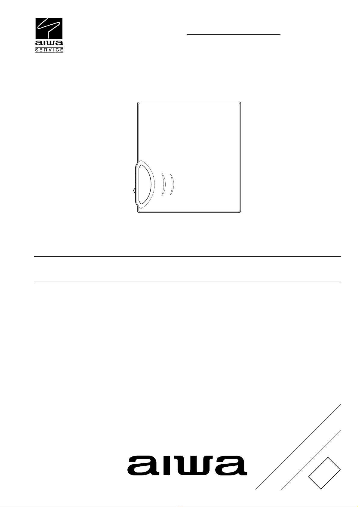
Aiwa AM-HX100 User manual

SERVICE MANUAL
DATA
MINIDISC PLAYER
AM-HX100
AHK
S/M Code No. 09-018-446-0R2
REVISION
BASIC MD MECHANISM: BZG-8 A
• This Service Manual is the “Revision Publishing” and replaces
“Simple Manual” of AM-HX100 <AHK>, (S/M Code No. 09-015-446-0T2).

2
SPECIFICATIONS
Main unit
Playback system MiniDisc digital audio system
Encoding methods ATRAC, ATRAC 3 LP2, ATRAC 3 LP4
Laser pickup Semiconductor laser
Sampling Frequency 44.1 Hz
Number of channels Stereo: 2 channels
Monaural: 1 channel
D/ converter 1-bit
Frequency response 40 20,000 Hz ± 4dB
20 20,000 Hz ± 1dB (10 ohms)
Wow and Flutter Below measurable limit
(± 0.001 % W.PEAK)
Output Phone jac
Maximum output level 8 mW + 8 mW (16 ohms)
Power requirements DC 1.2 V using the supplied Ni-MH
rechargeable battery
DC 1.5 V using an LR6 (size AA) dry
cell battery
AC house current using the supplied AC
adaptor and charger
Battery life POWER SAVE switch set to ON
(approx. hours)
SP LP2 LP4
Rechargeable 29 38 45
battery
LR6 (size AA) 40 72 75
al aline battery
Rechargeable 75 107 125
battery and LR6
al aline battery
POWER SAVE switch set to OFF
(approx. hours)
SP LP2 LP4
Rechargeable 22 24 27
battery
LR6 (size AA) 31 40 43
al aline battery
Rechargeable 55 66 68
battery and LR6
al aline battery
Maximum outside Approx. 71.1 (W) X 12.6 (H) X 77.2 (D) mm
dimensions (excluding projecting parts and controls)
Weight Approx. 56g, excluding batteries
< C adaptor C-D401 K>
Rated voltage AC 230 V, 50 Hz
Design and specifications are subject to change without notice.

– 3 –
CLASS 1 LASER PRODUCT
KLASSE 1 LASER PRODUKT
LUOKAN 1 LASER LAITE
KLASS 1 LASER APPARAT
This set employs laser. Therefore, be sure to follow carefully
the instructions below when servicing.
WARNING!!
WHEN SERVICING, DO NOT APPROACH THE LASER
EXIT WITH THE EYE TOO CLOSELY. IN CASE IT IS
NECESSARY TO CONFIRM LASER BEAM EMISSION.
BESURETOOBSERVEFROMADISTANCEOFMORE
THAN 30cm FROM THE SURFACE OF THE OBJEC-
TIVE LENS ON THE OPTICAL PICK-UP BLOCK.
sCaution: Invisible laser radiation when
open and interlocks defeated avoid
exposure to beam.
sAdvarsel: Usynliglaserstålingvedåbning,
nårsikkerhedsafbrydereerudeaffunktion.
Undgå udsættelse for stråling.
VAROITUS!
Laiteen Käyttäminen muulla kuin tässä käyttöohjeessa
mainitulla tavalla saataa altistaa käyt-täjän
turvallisuusluokan 1 ylittävälle näkymättömälle
lasersäteilylle.
VARNING!
Om apparaten används på annat sätt än vad som
specificeras i denna bruksanvising, kan användaren
utsättas för osynling laserstrålning, som överskrider
gränsen för laserklass 1.
PROTECTION OF EYES FROM LASER BEAM DURING SERVICING
CAUTION
Use of controls or adjustments or performance of proce-
dures other than those specified herin may result in
hazardous radiation exposure.
ATTENTION
L’utillisation de commandes, réglages ou procédures
autresque ceuxspécifiés peutentraîner unedangereuse
exposition aux radiations.
ADVARSEL
Usynliglaserstålingvedåbning,nårsikkerhedsafbrydereer
ude af funktion. Undgå udsættelse for stråling.
This Compact Disc player is classified as a CLASS 1
LASER product.
The CLASS 1 LASER PRODUCT label is located on the
rear exterior.
Precaution to replace Optical block
(KMS-330A)
Body or clothes electrostatic potential could
ruin laser diode in the optical block. Be sure
ground body and workbench, and use care the
clothes do not touch the diode.
1) After the connection, remove solder shown in
right figure.
PICK-UP Assy PWB
Solder

4
DISASSEMBLY INSTRUCTIONS
a
a
a
a
a
Removingonly thePANEL,BOT canmakethe serviceposition.
1. How to remove PANEL, BOT
(1) Remove the 5 screws a1-a5 (1.4-1.8) and the 2 screws b1,b2 (1.4-1.4).
(2) Take out PA EL, BOT.
* When assembling, put the PA EL, BOT from HP JACK side with care for strap hole and HOLD SW. Install the screws from 1 to 5 as shown in
the diagram.
2. How to remove PANEL, TOP
(1) Remove the 5 screws (a).
(2) Remove PA EL, TOP.
b2
a2
a1
a5
a4
a3
b1

5
b
cBOSS
BOSS
c
c
a
a
a
PICK UP
SHORT LAND
HINGE, BATT
3. How to remove HLDR, BATT/PWB, MAIN
(1) Short the PICKUP Shortland.
(2) Remove the solders of HI GE, BATT and disconnect the 3 connectors (a).
(3) Remove the screw at b, 3 screws at c and then take out PWB, MAI .
* Check that the 2 BOSS are inside the circuit board when assembling. Tighten the screw at b first.

6
BOSS
BOSS
BOSS
BOSS
BOSS
4. How to remove the mech nism nd FRAME, CENTER
(1) Remove the screw a and the HI GE, BATT.
(2) Remove the 5 BOSS and take out the mechanism.
* When assembling, make sure that all the BOSS are fixed.
HINGE, BATT
a

5. How to remove PICK-UP
(1) Remove the poly washer PW and then GEAR, A.
(2) Remove the screw a, and the SPR-P, LEAD.
(3) Remove the shaft and PICK-UP together.
a
PW GEAR, A
SPR-P, LEAD
PICK-UP
6. How to remove the SLED MOTOR
(1) Remove the poly washer PW and then GEAR, A.
(2) Remove the solder fixed at a.
(3) Remove the 2 screws at b and the SLED MOTOR.
a
b
PW
GEAR, A
SLED MOTOR

8
7. How to remove the SPINDLE MOTOR
(1) Remove the solder fixed at a.
(2) Remove the 3 screws at b1, b2 and b3 and SPI DLE MOTOR.
* Follow the direction of the arrow to tighten the screws from b1 onwards to install the SPI DLE MOTOR.
b3
a
b1
b2
SPINDLE MOTOR

– 9 –
ELECTRICAL MAIN PARTS LIST
DESCRIPTIONREF. NO. KANRI
NO.
PART NO. DESCRIPTIONREF. NO. KANRI
NO.
PART NO.
IC
87-A22-099-080 C-IC,LA9607T
87-A21-835-010 C-IC,LC896431
87-A21-526-010 C-IC,GM71VLS17403CTL-1
8B-HM4-603-010 C-IC,LC875164A-5V90
87-A22-051-040 C-IC,AK93C55BH
87-A21-038-040 C-IC,NJU7014R-TE2
87-A21-842-010 C-IC,CXA8110TQ
87-A22-057-080 C-IC,S-8328E20MC
87-A20-861-040 C-IC,S-80808ANNP
87-A21-566-040 C-IC,S-80820ANNP
87-017-596-080 C-IC,NJM2107F
87-A21-914-040 C-IC,XC6368B102MR
87-A21-341-040 C-IC,TA2131FL
87-A21-445-040 C-IC,TC7W66FK
87-A21-357-040 C-IC,AK4352VT
TRANSISTOR
87-026-645-080 C-TR,DTC144EE
87-A30-147-080 C-TR,2SA1832GR
89-115-884-080 CHIP -TRANSISTER 2SA1588Y
87-026-644-080 C-TR,DTA144EE
87-A30-604-080 C-FET,FDG311N
87-A30-261-080 C-FET,FDC633N
87-A30-606-080 C-FET,SSM6J06FU
89-332-654-080 C-TR,2SC3265Y
87-A30-605-080 C-FET,SSM3K05FU
87-A30-634-080 C-FET,SSM3J05FU
87-026-524-080 C-TR,HN1C03FUB
DIODE
87-017-850-080 C-DIODE,DAP222
87-A40-687-080 C-DIODE,M1FH3
87-A40-124-080 C-DIODE,RB501V-40
MAIN C.B
C101 87-A10-770-080 C-CAP,V 0.1-10 K B
C102 87-A10-765-080 C-CAP,V 0.033-10 K B
C103 87-A10-766-080 C-CAP,V 0.047-10 K B
C104 87-A10-765-080 C-CAP,V 0.033-10 K B
C105 87-A10-765-080 C-CAP,V 0.033-10 K B
C106 87-A10-765-080 C-CAP,V 0.033-10 K B
C107 87-A10-765-080 C-CAP,V 0.033-10 K B
C108 87-A10-531-080 C-CAP,V 10P-50 D CH
C109 87-A10-524-080 C-CAP,V 3.0P-50 C CH
C110 87-A11-170-080 C-CAP,S 4.7-6.3 K B
C111 87-A10-561-080 C-CAP,V 0.01-16 K B
C112 87-A10-561-080 C-CAP,V 0.01-16 K B
C113 87-A10-770-080 C-CAP,V 0.1-10 K B
C114 87-A10-770-080 C-CAP,V 0.1-10 K B
C115 87-A10-556-080 C-CAP,V 2200P-50 K B
C116 87-A11-049-080 C-CAP,U 1-6.3 K B
C117 87-A11-049-080 C-CAP,U 1-6.3 K B
C118 87-A11-050-080 C-CAP,TN 47U-4 M F95 A
C119 87-A11-049-080 C-CAP,U 1-6.3 K B
C120 87-A10-770-080 C-CAP,V 0.1-10 K B
C121 87-A11-170-080 C-CAP,S 4.7-6.3 K B
C122 87-A10-561-080 C-CAP,V 0.01-16 K B
C123 87-A10-554-080 C-CAP,V 1000P-50 K B
C124 87-A10-554-080 C-CAP,V 1000P-50 K B
C125 87-A10-770-080 C-CAP,V 0.1-10 K B
C126 87-A11-058-080 C-CAP,U 0.22-10 K B
C127 87-A11-049-080 C-CAP,U 1-6.3 K B
C200 87-A10-770-080 C-CAP,V 0.1-10 K B
C201 87-A11-170-080 C-CAP,S 4.7-6.3 K B
C202 87-A10-770-080 C-CAP,V 0.1-10 K B
C203 87-A10-758-080 C-CAP,V 3300P-50 K B
C204 87-A10-671-080 C-CAP,V 0.022-16 K B
C206 87-A10-770-080 C-CAP,V 0.1-10 K B
C208 87-A10-770-080 C-CAP,V 0.1-10 K B
C209 87-A10-770-080 C-CAP,V 0.1-10 K B
C212 87-A11-049-080 C-CAP,U 1-6.3 K B
C213 87-A10-556-080 C-CAP,V 2200P-50 K B
C216 87-A10-770-080 C-CAP,V 0.1-10 K B
C300 87-A11-049-080 C-CAP,U 1-6.3 K B
C301 87-A10-561-080 C-CAP,V 0.01-16 K B
C302 87-A10-561-080 C-CAP,V 0.01-16 K B
C303 87-A10-561-080 C-CAP,V 0.01-16 K B
C304 87-A10-561-080 C-CAP,V 0.01-16 K B
C305 87-A11-170-080 C-CAP,S 4.7-6.3 K B
C306 87-A10-561-080 C-CAP,V 0.01-16 K B
C307 87-A10-554-080 C-CAP,V 1000P-50 K B
C308 87-A10-770-080 C-CAP,V 0.1-10 K B
C400 87-A11-049-080 C-CAP,U 1-6.3 K B
C401 87-A11-049-080 C-CAP,U 1-6.3 K B
C402 87-A10-561-080 C-CAP,V 0.01-16 K B
C403 87-A10-561-080 C-CAP,V 0.01-16 K B
C404 87-A10-561-080 C-CAP,V 0.01-16 K B
C405 87-A11-049-080 C-CAP,U 1-6.3 K B
C406 87-A10-353-080 C-CAP,U0.22-10KB
C407 87-A10-353-080 C-CAP,U0.22-10KB
C408 87-A11-170-080 C-CAP,S 4.7-6.3 K B
C409 87-A10-591-080 C-CAP,TN 47-6.3 M F95-BCASE
C410 87-A10-902-080 C-CAP,U 0.47-10 K B
C411 87-A10-559-080 C-CAP,V 6800P-25 K B
C417 87-A11-170-080 C-CAP,S 4.7-6.3 K B
C600 87-A11-806-080 C-CAP,TN 47U-6.3 M PSLB
C601 87-A10-557-080 C-CAP,V 3300P-25 K B
C602 87-A11-806-080 C-CAP,TN 47U-6.3 M PSLB
C603 87-A10-770-080 C-CAP,V 0.1-10 K B
C604 87-A10-770-080 C-CAP,V 0.1-10 K B
C606 87-A11-170-080 C-CAP,S 4.7-6.3 K B
C607 87-A11-049-080 C-CAP,U 1-6.3 K B
C608 87-A11-751-080 C-CAP,TN 22U-4 M P
C609 87-A10-539-080 C-CAP,V 47P-50 J CH
C610 87-A10-663-080 C-CAP,V 270P-25 J CH
C611 87-A11-049-080 C-CAP,U 1-6.3 K B
C613 87-A11-049-080 C-CAP,U 1-6.3 K B
C614 87-A10-561-080 C-CAP,V 0.01-16 K B
C701 87-A10-770-080 C-CAP,V 0.1-10 K B
C702 87-A10-543-080 C-CAP,V 100P-50 J CH
C703 87-A10-543-080 C-CAP,V 100P-50 J CH
C704 87-A10-543-080 C-CAP,V 100P-50 J CH
C705 87-A10-543-080 C-CAP,V 100P-50 J CH
C706 87-A11-049-080 C-CAP,U 1-6.3 K B
C707 87-A11-170-080 C-CAP,S 4.7-6.3 K B
C708 87-A11-170-080 C-CAP,S 4.7-6.3 K B
C709 87-A11-058-080 C-CAP,U 0.22-10 K B
C710 87-A11-058-080 C-CAP,U 0.22-10 K B
C711 87-A11-049-080 C-CAP,U 1-6.3 K B
C712 87-A11-049-080 C-CAP,U 1-6.3 K B
C713 87-A11-170-080 C-CAP,S 4.7-6.3 K B
C715 87-A11-318-080 C-CAP,TN 220U-2.5 SVB2
C716 87-A11-318-080 C-CAP,TN 220U-2.5 SVB2
C717 87-A11-049-080 C-CAP,U 1-6.3 K B
C720 87-A11-058-080 C-CAP,U 0.22-10 K B
C721 87-A10-770-080 C-CAP,V 0.1-10 K B
C722 87-A11-170-080 C-CAP,S 4.7-6.3 K B
C723 87-A10-770-080 C-CAP,V 0.1-10 K B
C724 87-A11-049-080 C-CAP,U 1-6.3 K B
C725 87-A10-770-080 C-CAP,V 0.1-10 K B
C726 87-A10-770-080 C-CAP,V 0.1-10 K B
C728 87-A10-770-080 C-CAP,V 0.1-10 K B
C729 87-A11-049-080 C-CAP,U 1-6.3 K B
C750 87-016-449-080 C-CAP,TN 10-4 M S
C751 87-A10-770-080 C-CAP,V 0.1-10 K B

– 10 –
C752 87-A11-170-080 C-CAP,S 4.7-6.3 K B
C753 87-A11-170-080 C-CAP,S 4.7-6.3 K B
CN100 87-A61-315-080 C-CONN,20P H XF2L-2035
CN401 87-A61-316-080 C-CONN,8P H XF2L-0835
CN700 87-A61-317-080 C-CONN,8P H XF2L-0825
D300 87-A40-556-080 C-LED,CL-270HR RED
L100 87-A50-360-080 C-COIL, 47UH K NLFC252018
L101 87-003-245-080 C-COIL,2125 22UH K MLF2012
L200 87-003-245-080 C-COIL,2125 22UH K MLF2012
L300 87-005-769-080 C-COIL,2125 100UH K MLF2012
L400 87-A50-475-080 C-COIL, 10UH K NLFC201614
L401 87-A50-475-080 C-COIL, 10UH K NLFC201614
L402 87-A50-475-080 C-COIL, 10UH K NLFC201614
L403 87-A50-475-080 C-COIL, 10UH K NLFC201614
L404 87-A50-537-080 C-COIL, 100UH C4-K3L
L405 87-003-245-080 C-COIL,2125 22UH K MLF2012
L600 87-A50-324-080 C-COIL,47UH C4-K3L
L601 87-A50-012-080 C-COIL,100UH LQH3C
L701 87-005-769-080 C-COIL,2125 100UH K MLF2012
L750 87-003-245-080 C-COIL,2015 22UH K MLF2012
PR600 87-A91-769-080 C-PROTECTOR,0.75A ERY32SB075
PR601 87-A91-769-080 C-PROTECTOR,0.75A ERY32SB075
R224 87-A92-239-080 C-F-BEAD, BLM10A102SG
R305 87-A00-756-080 C-RES,V 10K-1/16W F
R306 87-A00-759-080 C-RES,V 27K-1/16W F
R331 87-A00-757-080 C-RES,V 12K-1/16W F
R332 87-A00-758-080 C-RES,V 22K-1/16W F
R334 87-A00-760-080 C-RES,V 68K-1/16W F
R335 87-A00-755-080 C-RES,V 6.8K-1/16W F
R615 87-A01-014-080 C-RES,V 330K-1/16W F
DESCRIPTIONREF. NO. KANRI
NO.
PART NO. DESCRIPTIONREF. NO. KANRI
NO.
PART NO.
R616 87-A01-015-080 C-RES,V 560K-1/16W F
R629 87-A01-013-080 C-RES,M/F V 220K-1/16W D
R630 87-A01-012-080 C-RES,M/F V 34K-1/16W D
R701 87-A91-879-080 C-F-BEAD, BK1608TS102
R702 87-A91-879-080 C-F-BEAD, BK1608TS102
R716 87-A91-879-080 C-F-BEAD, BK1608TS102
R717 87-A91-878-080 C-F-BEAD, BK1608HS241
R718 87-A91-878-080 C-F-BEAD, BK1608HS241
R719 87-A91-878-080 C-F-BEAD, BK1608HS241
R723 87-A91-879-080 C-F-BEAD, BK1608TS102
S300 87-A91-436-080 C-SW,PUSH 2-1-1 SPVE3.8
S301 87-A92-166-080 C-SW,SL 1-1-2 HSW4512-31
S302 87-A91-979-080 C-SW,TACT SOT-152HST
S303 87-A91-979-080 C-SW,TACT SOT-152HST
S304 87-A91-979-080 C-SW,TACT SOT-152HST
S305 87-A91-979-080 C-SW,TACT SOT-152HST
S306 87-A91-979-080 C-SW,TACT SOT-152HST
X200 87-A70-343-080 C-VIB,CER 16.934MHZ CSTCE
X300 87-A70-212-080 C-VIB,3.00MHZ PBRC-B
FLEX JACK C.B
8A-HM5-602-110 PWB,FLEX JACK
J700 87-A60-682-010 JACK,3.5 ST 7P
88
A
Resistor Code
Chip Resistor Part Coding
Figure
Value of resistor
Chip resistor
Wattage Type Tolerance
1/16W
1/10W
1/8W
1608
2125
3216
5%
5%
5%
CJ
CJ
CJ
Form
LW t
1.6 0.8 0.45
2 1.25 0.45
3.2 1.6
108
118
128
: A
: A
CHIP RESISTOR PART CODE
0.55
Resistor Code
Dimensions (mm)
Symbol
1/16W 1005 5% CJ
1.0 0.5 0.35 104
Lt
W
!
!

– 11 –
TRANSISTOR ILLUSTRATION
B
C
E
2SA1588Y
2SA1832GR
2SC3265Y
DTA144EE
DTC144EE
G
D
S
SSM3J05FU
SSM3K05FU FDC633N
FDG311N
SSM6J06FU
D1 G
D2
S
D4 D3
HN1C03FUB
E1 C2
B1
E2
C1 B2

WIRING – 1 (MAIN) <1 / 2>
1 2 3 4 5 6 7 8 9 1011121314151617181920212223242526272829303132
– 12 –
A
B
C
D
E
F
G
H
I
J
K
L
M
N
O
P
Q
R
S
T
U

WIRING 1 (MAIN) <2 / 2>
32 31 30 29 28 27 26 25 24 23 22 21 20 19 18 17 16 15 14 13 12 11 10 9 8 7 6 5 4 3 2 1
13
A
B
C
D
E
F
G
H
I
J
K
L
M
N
O
P
Q
R
S
T
U

14
SCHEMATIC DIAGRAM (MAIN / FLEX JACK)

WIRING 2 (FLEX JACK)
151413121110987654321
A
B
C
D
E
F
G
H
I
J
K
L
M
N
O
P
Q
R
S
T
U
15

16
IC BLOCK DIAGRAM

17
IC DESCRIPTION
IC, LC875164A-5V90
Pin No. Pin Name I/O Description
1 WSEL O Select signal terminal or writing lash memory (Normally L output).
2 WCLK O CLOCK terminal or writing lash memory (Normally L output). (Not used)
3 WDATA O DATA I/O terminal or writing lash memory (Normally L output). (Not used)
4 EMP I Electricity reduction interrupt input.
5 INTB I Interrupt request input rom LC896431.
6 CHG-INT I Interrupt request input rom battery charge stand loading cast (both edges).
7 ECO I Energy saving mode switch (interrupt eature possible).
8 RESET I Reset micro computer.
9 XT1 Connected to VDD.
10 XT2 Not used.
11 VSS1 Connected to GND.
12, 13 CF1, CF2 3MHz clock.
14 VDD1 Connected to VDD.
15 KEY0 I Main unit KEY A/D input.
16 KEY1 I Remote control KEY A/D input.
17 BATT I Power voltage A/D input.
18 VDET I For detecting V during charging.
19 BATT2 I Charged battery voltage A/D input.
20 ~ 22 NC Not connected.
23 PD O External DAC power down control.
24 PE O EEPROM error writing prevention port (L= disable write).
25 VDSW O ON/OFF control output or V detection ampli ier. L turns ON. H turns OFF.
26 CE3 O Chip select signal output o EEPROM (IC303).
27 CEQ O Chip select signal o LC896431.
28 DATA0 O Serial data output to LC896431.
29 DATAD I Serial data input rom LC896431.
30 SCK0 O Serial clock output to LC896431.
31 DATA2 O Serial data output to EEPROM.
32 DATAE I Serial data input rom EEPROM.
33 SCK2 O Serial clock output to EEPROM.
34 CE2 O Chip select signal output o EEPROM (IC301).
35 BEEP O BEEP signal output.
36 B-DISP1 O Battery remaining output 1. (Not used)
37 B-DISP2 O Battery remaining output 2. (Not used)
38 B-DISP3 O Battery remaining output 3. (Not used)
39 STALL O Power supply control output o motor driver.
40 NC Not connected.
41 SLPWM O PWM output or VM control o motor driver.
42 VDD Connected to VDD.
43 VSS Connected to GND.
44 KEY0 I Standby cancel signal input by the main unit KEY.
45 KEY1 I Standby cancel signal input by remote control KEY.

18
Pin No. Pin Name I/O Description
46 FOK I FOK signal input.
47 VP I VP (CLV servo lock check) signal input.
48 MON3 I Monitor 3 signal input rom LC896431.
49 MON2 I Monitor 2 signal input rom LC896431.
50 MON1 I Monitor 1 signal input rom LC896431.
51 MON0 I Monitor 0 signal input rom LC896431.
52 DEFECT I DEFECT signal input.
53 PPIT I PPIT signal input.
54 READ O Output H when reading data.
55 PLG-I I Insertion detection signal input o head phone jack (L: inserted).
56 RESET O LC896431 reset signal output.
57 HOLDER I Holder OPEN (H)/CLOSE (L) signal input & standby release.
58 FSEQ I FSEQ signal input o LC896431.
59 SHOCK I SHOCK detection o LC896431.
60 WRQB I Signal input rom LC896431.
61 CHG-O O Battery charge stand control output.
62 NIHM-O O Battery charge output.
63 BSTSW O Head phone ampli ier bus boost ON/OFF switch (BST on with H).
64 BST2 O DSL 3 STEP switch output.
65 BST3 O DSL 3 STEP switch output.
66 HP/LINE O Head phone ampli ier/line switch output.
67 LED1 O Operation LED control signal output (LED on with H).
68 VSS3 Connected to GND.
69 VDD3 Connected to VDD.
70 CHG-1 O Battery charge stand LED control output.
71, 72 NC Not connected.
73 P-CONT O System power supply control (L: turn on the power supply).
74 AMUTE O AUDIO MUTE signal output (H: turn on MUTE).
75 RMCDT O Serial data output to liquid crystal remote controller.
76 PWSTB O Standby signal output o headphone driver (L: standby).
77 DNSW O L when BATT is above 1.8V. H when CHGINT = L.
78 DRAMSW O Power supply control output o DRAM (L: turn on the power supply o DRAM).
79 JAPAN I Domestic/Overseas version switch input (H: domestic).
80 TEST I Test mode/Main mode switch input (L: test mode).

19
Pin No. Pin Name I/O Description
1 VCC2 Power supply output.
2 SHOCK O SHOCK/RFNG output terminal.
3 SLCO O Slice level output terminal o HF signal.
4 SLCIST I Bias resistance terminal o slice level adjustment ampli ier.
5 EFMIN I HF signal input terminal.
6 RESET I System Reset.
7 HFL I Track detection signal input terminal.
8 TEST2 I Test input terminal. (Connected to VCC)
9 PDO O Electric current charging pump output terminal o VCEC.
10 VCVSS Ground terminal or VCEC.
11 FR I Bias resistance terminal o VCEC oscillation requency.
12 ISET I Bias resistance terminal o VCEC electric current charging pump.
13 VCVDD Power supply terminal or VCEC.
14 AVSS1 Ground terminal or digital servo.
15 PEAK I PEAK signal input terminal.
16 BOTTOM I BOTTOM signal input terminal.
17 ABCD I Main beam light amount o signal input terminal.
18 TE I Tracking error signal input.
19 FE I Focus error signal input terminal.
20 VC I Intermediate electric potential input terminal.
21 AVDD1 Power supply terminal or digital servo.
22 DSW1 O Disc mode switch output.
23 DSW0 O Disc mode switch output.
24 SGC O AGC control signal output terminal.
25 AOFFSET O ABCD o set control signal output terminal.
26 FOFFSET O Focus o set control signal output terminal.
27 TOFFSET O Tracking o set control signal output terminal.
28 TBAL O Tracking balance control signal output terminal.
29 LDREF O Laser control signal output.
30 VSS Ground terminal.
31 VDD Internal power supply terminal.
32 FBAL O Focus balance control signal output terminal. (Not used)
33 SPPWMF O Spindle PWM output.
34 SPPWMR O Spindle PWM output.
35 MD7
I/O Data input and output terminal to DRAM. (Not used)
36 MD6
37 MRAS I/O Data input and output terminal to DRAM.
38 MWE I/O Data input and output terminal to DRAM.
39 VCC2 Power supply terminal.
40 MD1 I/O Data input and output terminal to DRAM.
41 NC O Not connected.
42 MD0 I/O Data input and output terminal to DRAM.
IC, LC896431

20
Pin No. Pin Name I/O Description
43 NC I/O Not connected.
44 PCK O VCEC system clock signal output terminal. (Not used)
45 VCC2 Power supply terminal.
46 VSS Ground terminal.
47 DEFECT I/O De ect signal input and output terminal.
48 MD3 I/O Data input and output terminal to DRAM.
49 NC I/O Not connected.
50 MD2 I/O Data input and output terminal to DRAM.
51 NC I/O Not connected.
52 VSS Ground terminal.
53 MCAS O Data input and signal output terminal to DRAM.
54 MOE O Data input and signal output terminal to DRAM.
55 MD9
O Data input and signal output terminal to DRAM. (Not used)
56 MD8
57 ~ 59 S1 ~ S3 O Sled PWM output terminal.
60 VSS Ground terminal.
61 VCC2 Power supply terminal.
62 BEMFU I/O Sled control signal input and output terminal.
63 VDD Internal power supply terminal.
64 BEMFV
I Sled control signal input terminal.
65 BEMFW
66 FOPWMF O Focus PWM output terminal.
67 FOPWMR O Focus PWM output terminal.
68 TRPWMF O Tracking PWM output terminal.
69 TRPWMR O Tracking PWM output terminal.
70 FG I Speed pulse input terminal.
71 VP O LCV servo lock recognition output.
72 FOK O Focus OK signal output terminal.
73 FAST O FAST signal output terminal. (Not used)
74 CL I Data trans er clock input terminal or CPU inter ace.
75 CE I Chip enable signal input terminal or CPU inter ace.
76 DI I Data input terminal or CPU inter ace.
77 DO O Data output terminal or CPU inter ace.
78 WRQ O Interrupt signal output terminal or CPU inter ace.
79 INT O Interrupt signal output terminal or CPU inter ace.
80 FSEQ O Frame period detection signal output.
81 F16M I 16.934 MHz input terminal.
82 ENH O De-emphasis indicator output.
83 LRCO O LR clock output.
84 DDATA O Expanded audio data output.
85 BCO O Bit clock output.
86 DDOUT O Digital audio output. (Not used)
Table of contents
Other Aiwa Mini Disc Player manuals