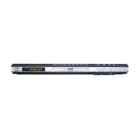
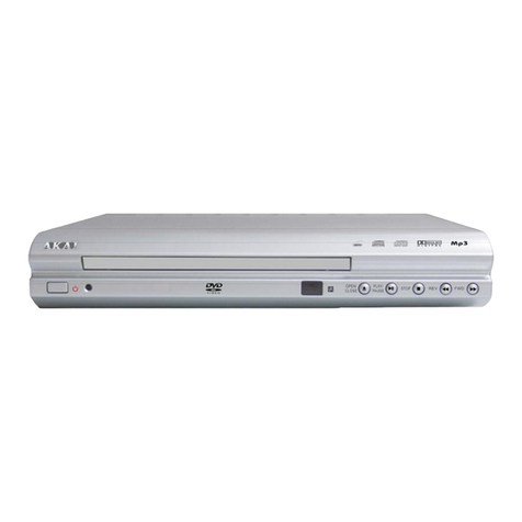
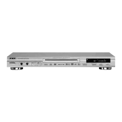
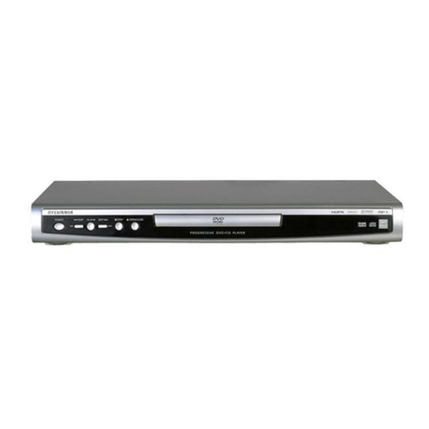
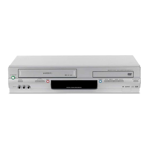
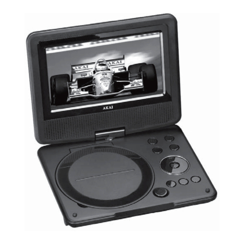
Akai DV-R4015VSS User manual

SERVICE MANUAL
Model:
DVR4015VSS
DVD PLAYER
www.akai.ru

目录
▲ Safety information ----------------------------3
1.General guid-----------------------------3
2.Low zeta potential leaking inspection ---3
3.High zeta potential leaking inspection --3
▲ Device avoiding ES(Electric Susceptible)
Influence of ESD (Electric Susceptible
Discharge)-----------------------------------------3
▲ Technical specification ----------------------4
▲ Mechanical diagram ------------------ ------8
Mechanical Parts------------------------- 9
▲ Packing and accessories ---------------------10
▲ Disassemble and assemble-------------------11
1.Take out disc from trouble player ----11
2.PCB position ------------------------11
▲ Disassemble and assemble parts of the unit
-----------------------------------------------12
1.Can open the tray by electricity -----12
2.Can not open the tray by electricity --12
3.Assemble the unit -------------------12
▲ Attachment 1----------------- 13
▲ Block Diagram/Electric circuit diagram
1.Block diagram ------------------------14
2.Electric circuit diagram ---------------15
3.Decoder board diagram ---------------16
4.AV output board diagram -------------20
5.Control board diagram ----------------23
▲ Attachment 2------------------24
▲ PCB Diagram
1.Upper decode board PCB diagram ----25
2.Lower decoder board PCB diagram ---26
3.AV output board PCB diagram --------27
4.Control board PCB diagram -----30
▲ Attachment 3---------------------------32
▲ Component list
1.AV output board component list --------33
2.Decoder board component list ----------36
3.Control board component list -----------39

SAFETY INFORMATION
General guide
1.Observe the original circuit during maintenance. if short
circuit occurs, change the over-hot or damaged components.
2.Observe all the protective device after maintenance, such
as whether the shielding cover or paper is assembled well.
3.To avoid electric shock, please inspect electricity leakage
aftermaintenance
Low zeta potential leaking inspection
1.Take out AC cord and connect a piece of wire between two
legsoftheoutlet.
2.Use Gear R x 10K of the voltmeter to measure the spares
on AC outlet and exposed metallic part with short circuit.
The resistance between screw cap, control shaft should be
unlimited.
Ω
uF
AC voltage table
to have discover metal
accessory of equipment
creepage checking circuit
cold water
canal(earthing)
picture 1
High zeta potential leakage inspection
.As illustrated 1, Connect Resistor with 1.5K, 10W and
capacitor 0.15 between exposed metallic part and device of
fine connection to the earth (water pipe etc.).
2.Plug-in AC cord directly to AC outlet. Do not inspect with
shield adaptor.
3.Utilize 1000 or more sensitive voltmeter to measure
alternating voltage.
4.Turn back the AC plug-in from AC outlet then iterate the
inspection as above.
5.Inspect the voltage of the resistor between other exposed
metallic parts and the earth with the same way.
6. The voltage must not be over than 0.75Vrms at any points
on the resistor. Electric leakage should not be over 0.5mA
when processing high voltage leakage testing through
Device avoiding ES(Electric Susceptible)
8. When disassembling and replacing the ES device, try to
reduce body movement (Or, the movement of legs, the
friction of fibrous of clothes, or elevating the legs from the
floor will generate static electricity ESD, causing damage to
the ES device.).
Influence of ESD (Electric Susceptible Discharge
exceeded the restrained figure, electric shock should be
possibly suffered. Do maintain the unit and inspect once
more before return to the user.
Device avoiding ES influence of ESD.
Some solid semi-conductor devices are easy to be
damaged by static electricity. These devices are generally
called ES device. The typical devices are IC, field effect
component and semi-conductor laser diode.
The following technology helps to abate the danger of
ESD on body before handle any semi-conductor or
semi-conductor component. Or wear the ESD bangle availed
from the market to eliminate the threaten of static electricity
on human body.
2.Put the electronic parts with ES device on the surface of
conductor such as aluminium foil after take them out in order
to protect static electricity from accumulation and explosion.
3.Solder or disassemble ES device through iron connecting
the earth.
4. Utilize device only anti-static electricity to disassemble
soldering tin. Non-anti static electricity device (ESC
protection) will release ES that damage ES device.
5.Do not use chemical volatile releasing static electricity
that leads to damage ES device
6. Unless preparation for pre-assembling has been made, do
not take out the ES device to be changed from the protective
packing ( most of the changed ES devices are packed
together with anti-static electrical foam or similar electric
material, besides, countermeasures for down-lead short
circuit are taken.).
7. Protective material should connect the model or the circuit
component to be assembled in it before taking out the
protective material from the ES device.
Note: do not bear electricity to the model or the circuit, and
pay attention to all the other safety information.
1

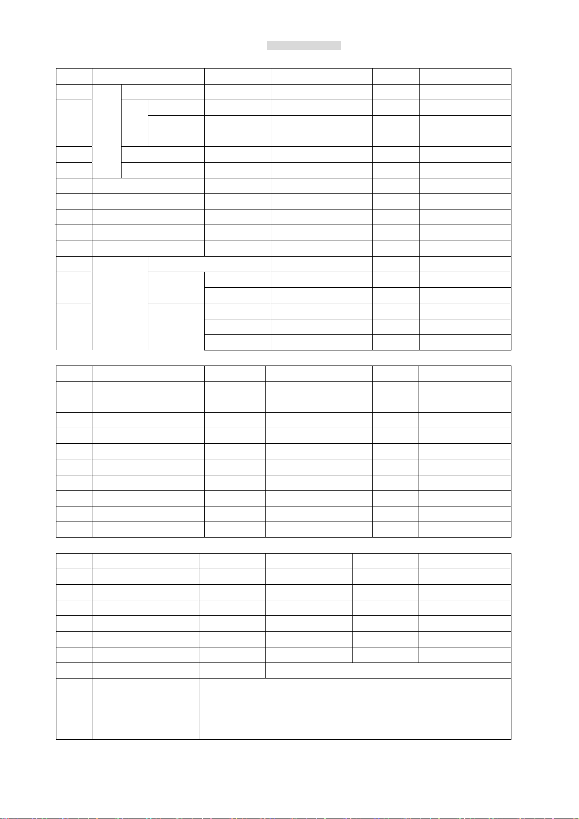
Technical specification
DVD Electric gudideline 1:Video parts
NO. Test items Test point Performance request Units Remake
1 video 1.0±0.2 Vp-p
Y 0.7±0.14 Vp-p
chroma 0.88±0.176 Vp-p
2
S-vid
eo C
Color sync 0.3±0.06 Vp-p
3 Y.Cr. Cb/Y.Pr.Pb 0.7+/-0.14 Vp-p
4
Output
range
R.G.B 0.7+/-0.14 Vp-p
5 Level definition ≥450 lines
6 bandwidth(+3/-6 dB) ≥5.5 MHz 100KHz 0 dB
7 differential coefficient bit DP ≤2 degree 75Ω loads
8 Lum non distortion ≤5 % 75Ω loads
9 Differential plus DG ≤2 % 75Ω loads
10 Y ≥56 (except power) dB 75Ω loads
U channel ≥50 dB 75Ω loads
11 C
V channel ≥50 dB 75Ω loads
R channel ≥50 dB 75Ω loads
G channel ≥50 dB 75Ω loads
12
S/N ratio
R
G
B B channel ≥50 dB 75Ω loads
2:Audio(Test signals:TCD-784)
NO. Test items Test point Performance request Units Remark
1
Lines audio input, output levels
1.8+0.2/-0.8 Vrms
DVD(LPCM)、CD
Audio input impedance:10KΩ
2 Breadth rage response ± 1.5 dB DVD(LPCM) 20Hz~20KHz
3 S/N ≥80 dB A count power
4 THD 10 % 1KHz A count power 10W
5 Condition areas 90 dB 1KHz A count power
6 Separate degree 70 dB 1KHz A count power
7 Channel inbalance ≤1.0 dB DVD(LPCM)、CD
8 Coaxial output range 0.5±20% Vp-p 75Ω± 1% loads
9 Optical output wavelengh (λp) 660±30 nm
3:Other characteristic parts
NO. Test items Test point Capability request Units Remark
1 Load time 10 S
2 Remote control for instance ≥5 m Front surface±15°areas
3 Input power voltage 230V±10% 50Hz
4 Expend power 110W Normal works
5 Deposited condition of temperature -25~+55 °C
6 Works condition of temperature 0~+40 °C
7 Freedom lower Accord GB/T 2423.8-1995 request
8 Disc formats
(1)DVD:
12cm single side, single layer;12cm single face, double layer;12cm double face. Double layer;
8cm single face, single layer; 8cm single face, double layer;8cm double face, double layer.
(2)CD disc:12cm disc,8cm disc
4:Test condition1.condition:normal temperature,normal voltage 2.power voltage:AC 230V 50Hz
3. speaker impedance: 8Ω
4

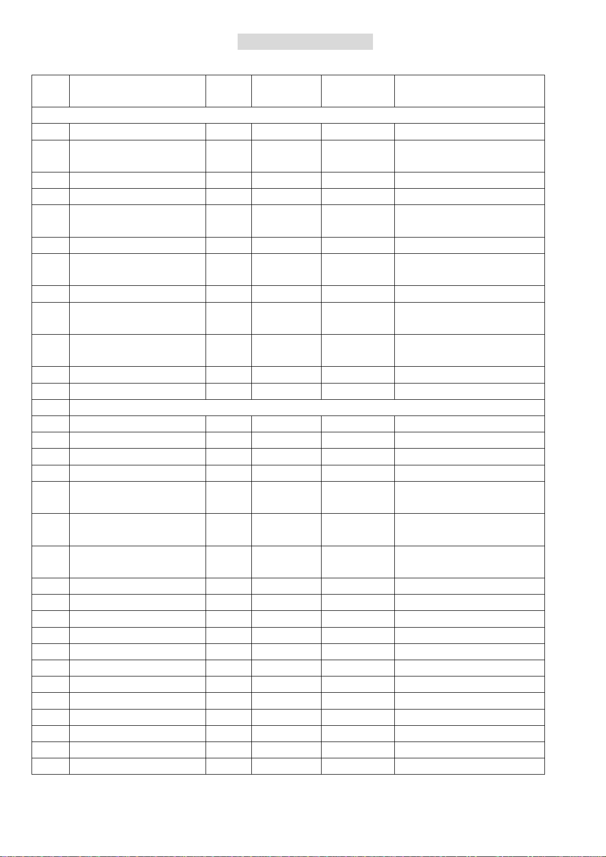
Technical specification
AVoutputboardelectricguidelineproductionmodel:AKAI DV-R4015VSS
Items Unit Model
Value
Limited
value
Test condition
POWER PARTS
1 Input voltage areas VAC 230±10%
2 Rating output voltage
and current
+5V 1.3A +5V 1.5A
-16V 2.2A +16V 3A
-16V 2.2A +16V 3A
AC3.7V
100mA
AC3.7V
120mA
-24V 50mA -24V 50mA
3 The least of output
power
W 110 Input voltage AC230 ±
10%V
4 +5 output veins wave mV <50
4 Power tune rate(+5V
port)
% 5 Input voltage AC230 ±
10%V
6 Loads tune rate(+5V
port)
% 5 current10mA-1.5A
AV output parts
7 Works voltage V ±16 ±20 RL=8Ω
8 Static state current mA 380 630
9 Output power W 12 14 THD = 10% RL = 8Ω
10 (FR/FL/SR/SL/CENT) 9 11 THD = 1% RL = 8Ω
11 Subwoofer output
power
W 30 35 THD = 10% RL = 8Ω
12 After all humorous
wave distortion
% 0.03 0.07 RL = 8Ω ; PO = 1W; f = 1KHz
0.7 RL = 8Ω ;PO = 0.1 to 7W;f = 100Hz to
15KHz
13 Bunch sound dB 70 f = 1KHz
60 50 f = 10KHz
14 S/N dB 80 75 A count power
15 Breadth response dB ±1.5 40~18KHz
5

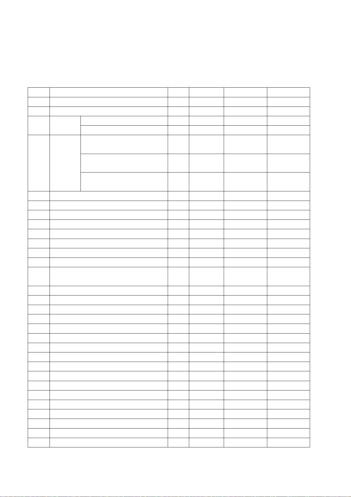
Electric Specification book
FM electric guideline Model:AKAI DV-R4015VSS
Test condition:
1.power supply voltage: AC 230V 50Hz 2.standard
output power: 1W
3.sound speaker impedance: 8Ω
4.standard confection: 1000Hz 22.5 KHz frequency deflection 5.Aerials impedance:75Ω
NO. Test items units Standard Limited Error
1 Intermediate frequency MHz 10.7 +/-0.1
2 Cover with areas MHz 87.5- 108 +/-0.1
90MHz KHz
3 Graduation
error 106MHz KHz
90MHz 22.5KHz frequency
deflection S/N 30dB
dBµV ≤26 ≤32
98MHz 22.5KHz frequency
deflection S/N 30dB
dBµV ≤26 ≤32
4 Chirp
limited is
sensitive to
degree
106MHz 22.5KHz frequency
deflection S/N 30dB
dBµV ≤26 ≤32
5 S/N ratio (98MHz,input 1mV except power)dB ≥50 ≥34
6 -3dB Limited delicacy degree µV 10 20
7 Intermediate frequency restrain(90MHz)dB 50 45
8 Lens restrain compete(106MHz)dB 28 22
9 Distortion degree(1mV input)% 0.6 1.5
10 Confection AC sound(input 5mV) dB 50 40
11 AFC areas(1mV input,-3dB) KHz
12 AM restrain(1mv input, confection degree 30%) dB 32 26
13 Output power (distortion10%,60Khzfrequency
leaning, 1mv input)
W 10
14 Breadth response(-3dB) Hz 40Hz-12.5KHz 100Hz-8KHz
15 The lease of volume mV 1 3
16 Locking station delicacy degree dB ≥28
17 separate degree dB 25 20
6

Electric Specification book
Mw electric guideline Model:AKAI DV-R4015VSS
Testcondition:
1.power supply voltage: AC 230V 50Hz 2.standard output power:1W
3.loundspeaker impedance: 8Ω4.standard confection: 400Hz 30% confection degree
No
. Test Items Unit Standard Limited Error
1 Intermediate frequency KHz 450 +/-3
2 Cover with areas KHz 522-1620 +/-5
S/N 20dB, 612KHz dBµV/M ≤75
S/N 20dB, 999KHz dBµV/M ≤70 ≤75
4 Chirp limited is
sensitive to degree S/N 20dB,1413KHz dBµV/M ≤70 ≤75
5 S/N SNR(999 KHz ,input 10mV/M, standard confection 1KHz A count power) dB ≥40 ≥34
6 Intermediate frequency restrain compete(612KHz)dB 45 35
7 Lens restrain compete(1413KHz)dB ≥34 ≥20
8 AFC(input100mV/M)dB 30 20
5mV/M input,30%confection degree % 1 3
9 Distortion
degree 100mV/M input,80%confection degree % 3 5
10 -6dBbandwidth (20dB S/N) KHz 8 5-10
11 whistle(input 5mV/M,IFx1 IFx2) % 3 10
Volume largest W
12 Output
power Distortion degree10% ,80% confection, input5mV/M W 10
13 +/-10KHz selectivity (on 1000KHz 20dB S/N) dB 14 8
14 Breadths response (-6 dB, input 5mV/M) Hz 40Hz-4KHz 100Hz-3.1
5KHz
15 Confection AC sound(input 100mV/M) dB 40 35
16 The least of volume yawp mV 1 3
17 Locking station delicacy degree dB ≤90
7

22
25
23
28
27
24
26
29
38
32
31
33
34
37
36
35
1
3
2
4
5
6
7
8
9
10
11
12
13
14
15
16
17
18
19
20
21
17
18
21
22
23
23
24
25
25 25
25
25
25
25
30
33
33
34
34
34
34
34
34
34
34
34
34
34
34
34
35
35
35
35
35
35
35
35
35
35
35
35
35
35
36
36
36 36
36
36
36
37
37
37
37
37
38
38
38
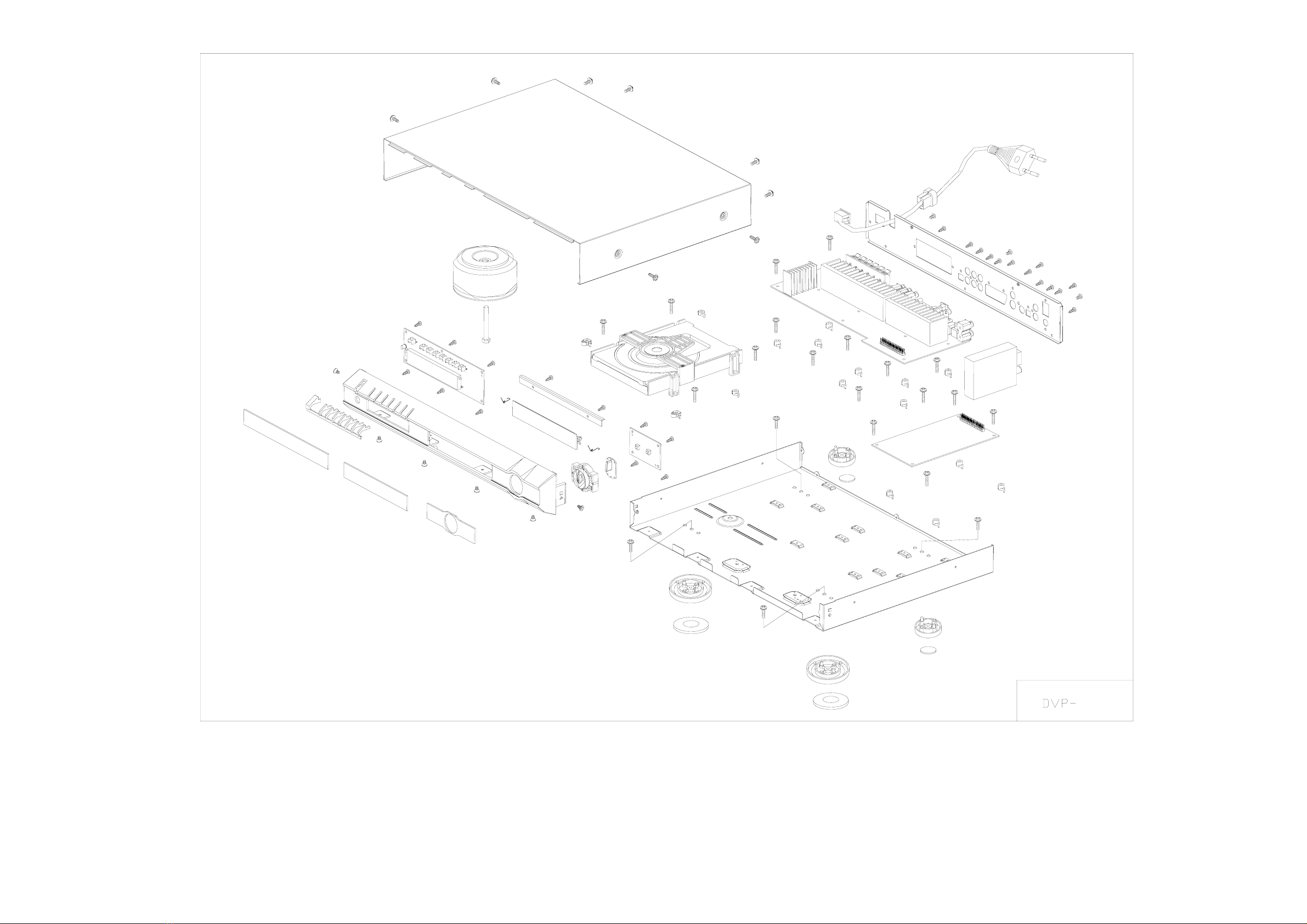
Mechanic parts of decompose diagram
8

9
37
38 N2-300812-14
32
33
36
35
34
N2-300614-54
N2-300815-54
N2-301215-54
N2-300812-19
WD-222232-01
N2-300615-54
ST3×8 PANi
PWTT3×6(adding forcedly)white
power cord2.2m 250V 2.5A VDE attention
PWB3×8(adding forcedly)white
PWTT3×12(adding forcedly)white
KTT3×6 sink head
PA3×8
26
27
28
31
30
29
Y6-440003-00
Q2-010120-16
S1-811048-01
A5-010120-20
A5-010120-10
A8-114100-20
21
20
22
23
25
24
Y3-030260-20
Y3-130151-20
Y3-130151-50
Q4-010120-00
Y3-130150-20
Y3-130150-50
power switchs PS8-11-D-048
line button SB4F-4
back baord
AV output board
decode board
Incept nog
back feet
PCB mat
back feet mat
front feet
motherboard
front feet mat
surface、motherboard
feet/motherboard
4
LianDong company(pin) HengZhiQian(lines)
motherboard/back surface
uuper cover/motherboard
decode board、output board、core/motherboard
control board,back port
8
6
17
3
25
1
HuaJie company
electrolyte board
power cord and back board
KST-MV114MA1-B0
1
1
1
1
1
1
1mm electrolyte board
sponge
ABS
ABS
2
13
2
sponge
ABS
2
2
Lead
7Y9-01016C-20
16
15
17
18
19
14
Y3-01016C-24
Y3-140160-20
Q3-050121-00
N4-230101-L0
N4-230101-R0
N2-604829-79
8
11
10
12
13
9
A6-000000-41
A5-010120-41
T1-400022-00
A5-010120-40
Q1-0101D0-04
Y3-060160-10
door spring(right)
transformer sleeping bolt K60×48
PCB plank(core using)
core plank
uuper cover board
door spring(left)
round power transformer
uuper cover board plank
control board
core
control board
disc tray
MATERIAL NO.
MACHINE PARTS OF COMPONENT LIST
NO.
3
4
6
5
2
Y9-01012C-31
Q1-010120-14
Y1-010171-00
Y1-0101G1-00
Y9-01012C-33
Y9-01012C-32
APPELLATION
Lens2
7KEY key
Vol button
surface
Lens1
Lens3
ACRYL
ABS
ABS
2
2
carbon wires
carbon wires
1
1
1
SONY optics head,RongXinDa plank
cool roll baord
1
1
1
ABS
1
PVC
1
ABS
ABS
ABS
REMARK
PVC
PVC
1
1
QTY

10
2.MATERIAL LIST
5O7-010120-R0
NO.
4
3
2
1
O7-010120-L0
O1-500600-10
A1-010120-10
Serial No.
O6-010121-00
42
sparking glue(right)1
mainframe bage 500*600mm
Appellation and Specification
sparkling glue(left)
remote control
white box
1
1
1
QTY
1
1
1.Decompose diagram
3
PACKING AND ACCESSORY
6
5

11
2.Wring 3 screws out connected base panel with bottom
board then wrest 4 screws connected loader with bottom
board(Diagram B)
3.Take out front panel and loader carefully,There is a white
plastic gear under the loader,Rotate the rear as diagram C to
stretch DVD tray and door(diagram D),you can take disc out
carefully.
Diagram B Panel,core disassemble front control board
Diagram H Boards Location
decode board
Per PCB assemblies locate as(see Diagram H)
AV output board
PCB position
If you cannot take out disc even press OPEN/CLOSE
button,please pull power cord from the socket and
follow as below:
1.Wring 8 screws out then pull left and right side
to take away top panel that rear part is upper
(Diagram A)
Diagram A Dipart cabinet
Diagram D Take out disc
Diagram C Rotate white gear
Take out disc by truble unit
fr
The unit comprises mechanical and electric part,including:
ont panel,base panel,top panel,bck panel and loader,AV
tput board,decode board,etc.
DISASSEMBLE AND ASSEMBLE
ou
White Gear

12
Can not open tray by electricity
Unable to open disc tray when press OPEN/CLOSE button
1. Take down disc as illustrated A,B,C,D
2. Take down DVD front panel
Can open the tray by electricity
1. Operate after completely take out top panel
2. Press OPEN/CLOSE button to open disc tray.
Be careful not to damage disc when take it out if it is in the tray .
Then take away DVD door (as illustrated E)
Graph E Catch position on the front panel
Catch
Catch
Catch
1. Take down top panel see as illustrate A
2.Take down front panel
Disassemble and assemble parts of the unit

Attachment 1:Block diagram、Circuit diagram
Block diagram
Circuit diagram
Decoder board circuit diagram
AV Output board circuit diagram
Control board circuit diagram
13

AKAI DV-R4015VSS Block diagram
14
5.1CH
audio
AV
output
power
transformer
AV output board parts
sound
box
system
FM/AM
receiving
nog
POWER
PARTS
front control baord(VFD
display)+remote receiving load
disc
digitals
audio
input、
output
complex video、S
-video、21PIN、
Chromatic
aberration
MTK
1379GE/C
+1336E/C
+SONY280
core(no takes
servo system)
decode and
data disposing

A
USE 1336E/C
TRSO
MDI1
RFL
C31:1336E/C = 82PF
RFOP
V2P8
H
+
C12
100UF
( B )
LIMIT
CB21
0.1uF
FMSO [ 3 ]
RFOP
E
C40 10pF
TP28 TEO1
TROUT
SL+
RVCCIN
SP-
A
R31
10k
GND
FOSO [ 3 ]
PWMOUT2
C31 390p
DMSO [ 3 ]
URST
CB55
0.1uF
R4 100K
R33 10k
RFRP
VR-DVD
AVCC
ADIN [ 3 ]
RFON [ 3 ]
V1P4
+
C1
100UF
CB12
0.1uF
TOP SIDE CONTACTED
( D )
V2P8 [ 3 ]
TRCLOSE
LOAD-
L22 FB,0805
USE 1336E
C41 27p
L24 FB,0805
FEO
CB35
0.1uF
R86
10K
C9 C
TRSO [ 3 ]
OP-
L21 FB,0805
SCLK [ 3 ]
ADIN
R38
100
1336E/C USE 4.7 OHM
A
S33
CB68
0.1uF
R11 10k
CSO
R24
10k
S33
+
C10
100UF
R2 750k
STBY
TRIN
CB34
0.1uF
R71
330k
RFVCC
R74
750k
VR-CD
+
C19
47UF
MT1336E
RFL
F+
R6 10K
R93
20k
USE 1336E/C SHOULD TO OPEN
( A )
FOSO
OP+
LIMIT
C8 1UF
L23 FB,0805
C85
150p
MT1336E&1336E/C+1379 with SONY 280 PUH.
Q5
3904
CB33
0.1uF
U4
BA6208F
1
2
3
4 5
6
7
8
VCC
BOUT
GND
AOUT BIN
NC
GND
AIN
Q3
2SK3018
2
3 1
Q4
2SK3018
2
3 1
R23 10k
SW1
CB66
0.1uF
AVCC
V1P4
TEO
TP31 FEO1
ASSEMBLE L2,L221,L23
RVCCIN
V1P4
Q2
2SB1132
F
B
C38
0.033uF
+
C47
47UF
VCC
RFON
C
URST
HTRC
J2
TRAY IN / OUT,5P,2.0 m/m
5
4
3
2
1
PWMOUT2
LDO1
LDO1
F
+
C18
47UF
R60
1
SMD 0805
HTRC [ 3 ]
TRIN
TROPEN
VCC
SP-
TRCLOSE
USE 1336E/C
STBY
LDO2
C
GND
R59
1
SMD 0805
FOSO
SDEN
AVCC
RVCCIN
SDATA [ 3 ]
CSO
MDI1 C39
470p
C6 1uF
C32 0.015uF
URST [ 2 ]
CB13 0.1uF
+
C20
10UF
R127
1K
CB32
0.1uF
RFRP [ 3 ]
C37 390p
( E )
PWMOUT2 [ 3 ]
D
IOA
R5 100K
CB29
0.1uF
TROPEN [ 3 ]
BDO
TP26 LRFRP1
R21 R
R35 27k
SDEN [ 3 ]
E
U10
BA5954
1
9
10
12
3
2
15
7
14
13
21
19
20
24
27
6
4
5
28
8
11
17
18
16
23
22
25
26
2930
VINFC
PVCC1
PGND
VOSL+
CF2
CF1
VOTK+
VNFFC
VOFC+
VOFC-
PVCC2
PGND
VNFTK
CTK2
BIAS
VOSL
VINSL+
VINSL-
STBY
VCC
VOSL-
VOLD+
VOLD-
VOTK-
VINLD
PREGND
CTK1
VINTK
G1G2
B
(A): CB7 = 470PF (MT1336E/C-PIN84)
CB11
0.1uF
TROPEN
V20
AA
OP-
B
R8 10K
CB31 0.1uF
R58
1
SMD 0805
SW1
RFO
T+
C147
0.015uF
ENDM
SP+
CB9 0.1uF
Reserved
FMSO
DD
C
BB
C
S33
L4
10uH,DIP
TEO
TROPEN
R7 33k
SL+
V1P4
V1P4
RFON
ENDM
( C )
CB30 0.1uF
F-
R102 20K
BOTTOM
CON1
HEADER 26 SMD0.5 BOTTOM
H26S/P0.5
1
2
3
4
5
6
7
8
9
10
11
12
13
14
15
16
17
18
19
20
21
22
23
24
25
26
DMSO
LDO2
H
OP+
RFO
R92 10k
1336E/C USE 470P
V2P8
TROUT
SDATA
FEO
R34 100k
E
(B): R7 = 15K (MT1336E/C-PIN108)
SDEN
+
C68
10UF
CB7 0.1uF
C3 1uF
VCC
L1 FB,0805
TP25 HRFRP1
CB6 0.1uF
R85 20k
LDO_AVCC
IOA
RVCCIN
+
C67
100UF
1376 USE 15K OHM
FEO [ 3 ]
B
OPO
RFOP [ 3 ]
R15 22
R22 R
RFVCC
FMSO
OPO
C
R69 1
(C): R22 / R21 OPEN (MT1336E/C-PIN36/35)
V1P4 [ 3 ]
D
AVCC
TP30 RFL1
RFL [ 3 ]
+
C25
47UF
ADIN
V20
RVCCIN
SL-
CB2
0.1uF
ASSEMBLE L20,L21,L24
BDO [ 3 ]
CSO [ 3 ]
T-
+
C35
10UF
SCLK
STBY
L20 FB,0805
J5
SLED/6P,2.0mm
1
2
3
4
5
6
7
8
9
CB26
0.1uF
C2 1uF
(D): R35 / R34 OPEN (MT1336E/C-PIN32/27)
TEO [ 3 ]
DMSO
SCLK
LD-CD
C72
150p
L2 FB,0805
TP22SCLK1
G
L25 FB,0805
TP29 CSO1
BDO
WHEN USE 1336E/C RED COLOR CAN MOVE
SP+
SL-
CB8
0.1uF
TRCLOSE
G
CC
TP23 CRTP1
L5
10uH,DIP
: C41 / C40 / C39 OPEN (MT1336E/C-PIN32/28/27)
R14 22
U2
MT1336E
128
127
126
125
124
123
122
121
120
119
118
117
116
115
114
113
112
111
110
109
108
107
106
105
104
103
38
37
36
35
34
33
32
31
30
29
28
27
26
25
24
23
22
21
20
19
18
17
16
15
14
13
12
11
10
9
8
7
6
5
4
3
2
1
39
40
41
42
43
44
45
46
47
48
49
50
51
52
53
54
55
56
57
58
59
60
61
62
63
64
66
67
68
69
70
71
72
73
74
75
76
77
78
79
80
81
82
83
84
85
86
87
88
89
90
91
92
93
94
95
96
97
98
99
100
101
102
65
WGND
RFSUBO
LDO2
LDO1
MDI1
MDI2
AGC3
AGC2
WAVDD
AGC1
WGAND
SGND
TNI
TPI
SVDD
CDFON
CDFOP
SD
SC
AVDD
IR
AGND
SB
SA
MD
MC
VFO13
VDD
AGNDX
AGNDX
AGNDX
DPFO
DPFN
GNDP
HTRC
TRLP
TRLPA
CRTPLP
CRTP
HRFRP
LRFRP
DEFECT
VDDP
TEO
CSO
LVL
FEO
V20
VREFO
V2REFO
AVDDT
TM4
AGNDT
TM3
TM2
TM1
AGNDO
RFON
RFOP
AVDDO
AGNDX
AGNDX
WVDD
WOBSO
GND
UDGATE
HDGATE
IO0
IO1
IO2
IO3
IO4
IO5
IO6
IO7
IO8
IO9
IOA
IOB
VDDS
XCK16M
SCLK
GNDS
SDEN
SDATA
RST
DPDMUTE
AGNDP
AGNDX
AVDDP
VCON
AVDDF
AGNDX
AVDDM
COSPHI
HALLCOS
REFCOS
AGNDM
HALLSIN
REFSIN
SINPHI
SW0
SW2
SW1
MOP
MON
AGNDX
AGNDX
CEON
CEOP
RFGCI
RFGCU
RFFGC
OSP
OSN
CDD
CDC
CDB
CDA
DVDRFIN
DVDRFIP
DVDD
DVDC
DVDB
DVDA
MA
MB
AGNDF
C7 1uF
VCC
+5V
TRSO
LD-DVD
CB18
0.1uF
SDATA
+5V
CB10 0.1uF
USE 1336E SHOULD TO GND
C31:1336E = 390PF
VCC
HTRC
D
Q1
2SB1132
LOAD+
LDO_AVCC
R57
1
SMD 0805
CB19 0.1uF
R1 R
2SB1132
RFRP
R65
330k
CB22
0.1uF
CB5 0.1uF
(E): C31 = 82PF (MT1336E/C-PIN25)
Decode board elements diagram 1
16

S33
DQ[0..15]
W
R#
V25
TP4
XTALO
1
PLL_CLK [ 4 ]
FEO
RFOP
MA10
R11733
TP8RFON 1
S3.3V
FMSO
AV33
V1P4 [ 1 ]
FEO [ 1 ]
A0
S
CK
PLL-CE
CB42
0.1uF
R10 0
TROPEN [ 1]
RFON [ 1 ]RFON
Q
6
GND
VOL1
C50 0.01uF
PWMOUT2
RFL
Q
11
FS0
ACLK
FOSO
GND
Q
0
GND
U3B
74HC04
3 4
147
BDO
SDEN
SPLRCK
RESET#
R9 0
DCKE
VSDA
A7
GND
GND
TU_DATOUT [ 4 ]
DQM[0..3]
TP1 RFRPC
1
ASDAT[0..2] [ 4 ]
J3
1
2
3
4
5
6
7
8
9
Y[0..7] [ 4 ]
RGB_SWITCH [ 4 ]
TROPEN
VHSY
R468.2k
IIC
PRD# [ 3 ]
AMDAT
DA
Q
12
DV33
MA2
T
U
N
E
R
I
N
T
E
R
F
A
C
E
C
KE
C102
100p
GND
A15
Y1
C76
0.015uF
A16
W
E#
Y6
A8
CB37
0.1uF
V25
ABCK
RDS_CLK [ 4 ]
PCE#
PWR#
ABCK
SPBCLK
CB65
0.1uF
AUDIO INTERFACE
RDS-DAT [ 4 ]
+
C60
47uF
A[0..19] [ 3 ]
WE# [ 3 ]
only third over tone
TRSO
DCLK
RAS#
VOL1
+
C15
10UF
A3
Q
14
AD6
AV33
Y[0..7]
ASDAT0
AV33
SDA [ 4 ]
V1P4
HTRC
VOL2
Q
8
AD7
MA3
ACLK
SPBCLK
INT [ 4 ]
SCLK
A[0..19]
PRD#
C98100pF
RAS# [ 3 ]
A11
X
D
AD[0..7] [ 3 ]
RDS_LATCH [ 4 ]
V2P8
SDATA [ 1 ]
ALRCK [ 4 ]
CAS#
DV33
AD1
SDA
TU_DATOUT
CB70
0.1uF
RFIN
S
D
A
RxD
TP7RFDTSLVN 1
C105
100p
PCE# [ 3 ]
DV33
Q
10
RDS-LATCH
CB24 0.1uF
R53750k
R118 33
+5V
RFOP
ASPDIF
C
L
GND
XO
V25
S33
ADIN
Q
1
DV33
SPMCK [ 4 ]
C111
100p
CB53
0.1uF
A14
DV33
V25
SW-A
ACLK [ 4 ]
ADOUT [ 4 ]
AV33
BDO [ 1 ]
DMSO [ 1 ]
URST [ 1 ]
RFRP
ALRCK
LINE-IN
VOL2
R10833
R109 33
XTALI
HTRC
Y5
DACV33B
MEMORY
A18
SPDATA
+
C28
10UF
C26
15p
CSO [ 1 ]
SDA
CSO
C92100pF
R67 1K
C21
1000p
R11433
SW-B
A5
MA1
X
D
CB15
0.1uF
SPDATA [ 4 ]
CS#
MA[0..11]
RFIP
U3A
74HC04
1 2
147
CB47
0.1uF
SPLRCK [ 4 ]
ASDAT1
Q
3
C56 0.01uF
R96
4.7
R98 33
FS0 [ 4 ]
Q
13
MA6
VOL3
C48 1000pF
C81100pF
R10633
PWR# [ 3 ]
DCLK [ 3 ]
MUTE_DAC
C84
330pF
CB71
0.1uF
R52
4.7
L7 2.7uH, DIP
R126 33
DV33
TU_DATIN
C114
2.2UF
C86
330pF
R89
4.7
CB46
0.1uF
GND
R
D#
AD0
R39 18k
R9510k
C53 0.01uF
CB52
0.1uF
C95
100p
C520.01uF
CB44
0.1uF
SCL [ 4 ]
SPLRCK
C89100pF
CB67
0.1uF
NEAR PIN 212
SPBCLK [ 4 ]
DMSO
A
0
TP12 LPFIP1
CB51
0.1uF
CB25 0.1uF
MUTE_DAC [ 4 ]
V1P4
RFL
A1
URST
V25
FOSO [ 1 ]
CS# [ 3 ]
VSCK
DV33
L12
FB,0805
TP15 JITFN1
R115
1K
TP17 TRSO1
S
TB
A13
TP13 LPFOP1
C22
15p
A6
PWMOUT2
TP3 XTALI
1
AV33
Q
4
A17
HSYN
TEO
ASDAT[0..2]
TRSO
+
C33
10UF
C49 1000pF
C100100pF
ASPDIF [ 4 ]
A4
SPMCK
SW-B [ 4 ]
A
9
RDS-CLK
TP5RFDTSLVP 1
C34 1000pF
RESET# [ 4 ]
AD[0..7]
RESET#
FS
FLASH
FMSO [ 1 ]
V2P8 [ 1 ]
SDEN
Y2
C110
100pF
RFRP
A12
Q
7
BDO
SW-B
TP20 FMSO1
R27 100k
R120 33
URST
TU_STEREO
+
C43
10UF
C88
100p
ASPDIF
S
#
Q
15
SW-A
GND
C107100pF
FMSO
GND
BA[0..1] [ 3 ]
GND
RGB_SWITCH
L11
FB,0805
C78100pF
SW-A [ 4 ]
Y3
D3
1N4148
VIDEO INTERFACE
S33
A
11
TP9RFOP 1
R112 33
U3D
74HC04
9 8
147
PWMOUT2 [ 1 ]
CB59
0.1uF
RFOP [ 1 ]
RFL [ 1 ]
XTALI
VOL3
SPDATA
+
C42
10UF
R29 100k
A10
V1P4
ASDAT2
CB48
0.1uF
C4
2.2UF
INT
DQM0
DACV33C
URST
BA1
CSO
GND
RGB_SWITCH
VSTB
GND
RFRPC
DACV33A
TP14 JITFO1
R12233
TP16 FOSO1
RFRP [ 1 ]
R105 33
TU_STEREO [ 4 ]
AD2
U6
MT1379E
SMD LQFP-216
53
54
55
56
57
58
59
60
61
62
63
64
65
66
67
68
69
70
71
72
73
74
75
76
77
78
79
80
81
82
83
84
85
86
87
88
89
90
91
92
93
94
95
96
97
98
99
100
101
102
103
104
216
215
214
205
204
213
202
201
200
199
198
197
196
195
194
193
192
191
190
189
188
187
186
185
184
183
182
181
180
179
178
177
176
175
174
173
172
171
170
169
168
167
166
165
164
163
162
161
160
159
158
157
156
155
154
153
152
151
150
149
148
147
146
145
144
143
142
141
140
139
138
137
136
135
134
133
132
131
130
129
128
127
126
125
124
123
122
121
120
119
118
117
116
115
114
113
112
111
110
109
108
107
106
105
1
2
3
4
5
6
7
8
9
10
11
12
13
14
15
16
17
18
19
20
21
22
23
24
25
26
27
28
29
30
31
32
33
34
35
36
37
38
39
40
41
42
43
44
45
46
47
48
49
50
51
52
203
206
207
208
209
210
211
212
IOA20
APLLVSS
APLLVDD3
ALE
IOOE#
IOWR#
IOCS#
DVSS
UP1_2
UP1_3
UP1_4
UP1_5
UP1_6
DVDD3
UP1_7
UP3_0
UP3_1
INT0#
IR
DVDD2
UP3_4
UP3_5
UWR#
URD#
DVSS
RD7
RD6
RD5
RD4
DVDD2
RD3
RD2
RD1
RD0
RWE#
CAS#
RAS#
RCS#
BA0
DVSS
RD15
RD14
RD13
RD12
DVDD3
RD11
RD10
RD9
RD8
DVSS
CLK
CLE
RFIP
RFIN
RFDTSLVN
FEI
CSO
RFDTSLVP
TEZISLV
RFSUBI
ADIN
ADCVSS
BDO
SLCK
SDEN
SDATA
WOBSI
UDGATE
DVDD3
IDGATE
VFO13
DVSS
PRST
XTALI
XTALO
DVDD3
SPBCK
SPLRCK
DVDD2
SPDATA
SPMCLK
HSYN
DVSS
YUV7
VSYN
BLANK#
ICE
YUV6/R
YUV5/B
DACVSSA
YUV4/G
DACVDDA
YUV3/CVBS
DACVSSB
YUV2/Y
DACVDDB
YUV1/C
DACVSSC
YUV0/CIN
FS
VREF
DACVDDC
ASDATA4
ASDATA3
ASDATA2
ASDATA1
ASDATA0
SPDIF
MC_DATA
ACLK
DVDD3
ALRCK
ABCK
RD16
RD17
DVSS
RD18
RD19
RD20
RD21
DVDD2
RD22
RD23
DQM2
DQM3
DVSS
RD24
RD25
RD26
RD27
DVDD3
RD28
RD29
RD30
RD31
DVSS
RA3
RA2
RA1
RA0
DVDD2
RA10
BA1
DQM0
DQM1
DVSS
RA4
RA5
RA6
DVDD3
RA7
DMVSS
DMVDD3
RA8
RA9
RA11
IREF
PLLVSS
LPIOP
LPION
LPFON
LPFIP
LPFIN
LPFOP
JITFO
JITFN
PLLVDD3
FOO
TRO
TROPENPWM
PWMOUT1
PWMOUT2
DVDD2
DMO
FMO
DVSS
FG
HIGHA0
HIGHA1
HIGHA2
HIGHA3
HIGHA4
HIGHA5
DVSS
HIGHA6
HIGHA7
AD7
AD6
AD5
AD4
DVDD3
AD3
AD2
AD1
AD0
IOA0
IOA1
DVDD2
IOA2
IOA3
IOA4
IOA5
IOA6
IOA7
A16
A17
IOA18
IOA19
TEI
RFLEVEL
RFRP_DC
RFRP_AC
HRFZC
PWMVREF
PWM2VREF
ADCVDD3
R40 1K
TROPEN
R10118k
S33
DCKE [ 3 ]
TRSO [ 1 ]
FOSO
INT
R16
20k
CB36
0.1uF
TP2 HTRC
1
Q
2
AV33
DMSO
V25
R12533
C97
100p
C55100pF
BA[0..1]
SCL
ADIN [ 1 ]
A2
R
C
LK
V2P8
CB56
0.1uF
PLL_CE [ 4 ]
ADIN
Q
5
V25
C
E#
MA7
DACV33B
Y1 C27MHz
1 2
R90 33
CB74
0.1uF
FS0
GND
DQ[0..15] [ 3 ]
MA[0..11] [ 3 ]
A
S#
AD5
CB38
0.1uF
TP19 DMSO1
TP6 ADIN
1
MT1379_216
CAS# [ 3 ]
RFON
SDATA
DACV33A
S33
A19
LINE-IN
XI
WE#
MUTE_DAC
Q
9
DQM1
CB62
0.1uF
R47
390
MA4
V25
GND
SPMCK
R4315k
ABCK [ 4 ]
Y0
RDS-DATA
+
C51
10UF
L13
FB,0805
CB43
0.1uF
TU_DATIN [ 4 ]
A
8
SCLK
A
S#
FEO
MA0
R111
1K TxD
SDEN [ 1 ]
HTRC [ 1 ]
DQM[0..3] [ 3 ]
SDATA
AD4
R124.7K
J4
4 HEADER
1
2
3
4
TEO [ 1 ]
Y4
IR
DACV33C
A9
AD3
PLL-CLK
CB39
0.1uF
CB40
0.1uF
R28 10
CB72
0.1uF
TEO
SCLK [ 1 ]
SCL
MA5
R10320k
Decode board elements diagram 2
17

Decode board elements diagram 3
CAS#
FCE#
BA0
RDQM0
DMA5
RDQ7
DMA3
WE#[ 3 ]
MA[0..11]
RDQ11
A7
A14
FLASH_VCC
PCE#[ 2 ]
SDA DMA3
FWR#
DMA0
PWR#[ 2 ]
DQ4
RDQ10
DQ0
DMA2
A3
RDQ0
DMA7
A[0..19][ 2 ]
SCL
SDA
RDQ4
RDQ3
AD7
DWE#
SDCKE
A16
S3.3V
AD[0..7]
MA2
AD5
AD0
DQ7
DMA5
DRAS#
DQM[0..3]
DQ[0..15]
DCLK
MA11
DQ2
WE#
RDQ7
DBA1
RDQ15
RDQ9
+
C109
47u
RDQ5
RDQ8
DMA9
S33
RDQ5
DMA11
A5
A19
L16
FB / 0805 DQ9
RDQ2
DMA10
FLASH_VCC
AD6
RDQ14
S33
BA[0..1]
BA1
DMA6
DQ8
MA9
DQ5
MA5
SDCLK
DWE#
FCE#
A10 L14
FB / 0805
DQ3
RDQ2
DMA8
CB81
0.1u
+
C106
47u
DQM1
DQ1
RDQ9
MA1
8M Flash
PWR#
U14
EEPROM 24C02, ST-SO8
1
2
3
4
5
6
7
8NC
NC
NC
GND
SDA
SCL
WP
VCC
AD1
AD3
DMA1
CB80
0.1u
RAS#
RDQM1
DQM2
DMA11
R97 33
RDQ3
DMA1
A18
AD4 L15
FB / 0805
CB61
0.1u
+
C73
47u
RDQ1
RAS#
A15
FRD#
DCKE
A13
DCS#
CB69
0.1u
+5V
RDQ1
R123
10K
RDQ4
CB83
0.1u
RDQ15
PRD#
DQ13
RDQM2
R104 33
DQ10
MA7
DRAS#
CB77
0.1u
CB75
0.1u
SDCKE
PRD#
DMA9
CB76
0.1u
RN1 33x4
1 2
3 4
5 6
7 8
A[0..19]
DMA7
DMA8
RDQ10
DCLK
AD2
U15
SDRAM 1Mx16x4
1
2
4
12
5
7
9
8
10
46
11
13
15
16
17
18
19
35
22
23
24
25
26
14
41
29
30
31
32
33
34
36
37
38
39
40
43
42
44
52
45
47
49
48
50
51
53
54
20
21
3
6
27
28
VCC
DQ0
DQ1
VSSQ
DQ2
DQ3
VCCQ
DQ4
DQ5
VSSQ
DQ6
DQ7
DQML
WE
CAS
RAS
CS
A11
A10/AP
A0
A1
A2
A3
VCC
VSS
A4
A5
A6
A7
A8
A9
NC
CKE
CLK
DQMH
NC
VCCQ
DQ8
DQ9
VSSQ
DQ10
DQ11
VCCQ
DQ12
DQ13
DQ14
DQ15
VSS
BA0/A13
BA1/A12
VCCQ
VSSQ
VCC
VSS
U12
MX29F800T(TSOP-48)
1
2
3
4
5
6
7
8
9
10
11
12
13
14
15
16
17
18
19
20
21
22
23
24 25
26
27
28
29
30
31
32
33
34
35
36
37
38
39
40
41
42
43
44
45
46
47
48
A15
A14
A13
A12
A11
A10
A9
A8
NC1
NC2
WE
RESET
NC3
NC4
RYBY
A18
A17
A7
A6
A5
A4
A3
A2
A1 A0
CE
VSS1
OE
DQ0
DQ8
DQ1
DQ9
DQ2
DQ10
DQ3
DQ11
VCC
DQ4
DQ12
DQ5
DQ13
DQ6
DQ14
DQ7
DQ15/A-1
VSS2
BYTE
A16
SD3.3V DCAS#
A0
SCL
A17
FLASH_VCC
RDQ6
CS#
FWR#
RDQ11
DBA1
SDA[ 2 ]
CS#
DQ12
DCS#
SDCLK
A2
A8
A6
RDQ13
DQ15
FRD#
DQ14 RDQ13
MA8
MA0
DBA0
RDQM0
DCKE[ 2 ]
54-Pin TSOPII(400mil x 875mil)
DQM3
DCAS# SD33
DQ6
BA[0..1][ 2 ]
RDQ12
DMA0
RDQ8
DQM[0..3][ 2 ]
RDQM3
DCKE
DMA2
CAS#[ 3 ]
CS#[ 3 ]
SD3.3V
A11
DQ11
DMA4
RDQ6
AD[0..7][ 2 ]
DMA10
SCL[ 2 ]
PCE#
A4
A1
RDQM1
DBA0
MA6
DQM0
WE#
DMA4
CAS#
RDQ0
RDQ12
DQ[0..15][ 2 ]
PCE#
MA[0..11][ 2 ]
MA3
RAS#[ 3 ]
PWR#
A12
RDQ14
MA4
PRD#[ 2 ]
SD33
DCLK[ 2 ]
DMA6
MA10
A9
EliteMT M12L64164A-5T
18

A_MUTE[ 2 ]
INT[ 2 ]
+12V
D5
5.1V
R70
10K
+5VB
+
C104
10UF
+A5V
SL
R49
15k
+12VA
TUDAT_OUT
RESET#
R41
5.1k
+12V
+
C5
100u
S33
3904 / 3906
GND
only MTK1336E-C
DAC_LEF
TUVCC
COA
+
-
U5B
NJM4558
5
67
8 4
R13
33
RESET#
SW-B
+
C79
10UF
C59
2000p
CB89
0.1u
+
C11
47u
R99
10k
-12VA
DAC_FL
RESET#[ 2 ]
DAC_FL
ML
CB79
0.1uF
D4
5.1V
SPBCLK
Y1
D17
4148
CB20
0.1u
R84
10K
E
Y[0..7]
C65
2000p
D10
4148
LINE_IN[ 2 ]
SDAT2
TU-L
ABCK
J7
3
2
1
L19
R61 33
CB84
0.1u
-12VA
ADOUT
RDS_DATA
U1A
1117/3.3V
3
1
2
VI
GND
VO
CB49
0.1u
+
C90
10UF
+5VD
R56
10K CB17
0.1u
CB60
0.1UF
-12VA
RGB_SWITCH[ 2 ]
SACLK
-12V
C83
220p
L6
+
C93
10u
R18
4.7K
SOP8
+5V
SBCLK
AUX_L
GND
D11
4148
R72
10k
CEN
+
-
U7A
NJM4558
3
21
8 4
+
C30
100u
+12V
Y5
+12V
+
C75
47UF
-12V
TU-R
MUTE
only MTK1336E
DAC_FR
SPMCK
D8
4148
C71
220p
-12VA
SLRCK
Y[0..7][ 2 ]
+12VA
R19 2.2k
+
C101
10u
SPLRCK
R66 33
+
-
U5A
NJM4558
3
21
8 4
CB86
0.1u
ASPDIF[ 2 ]
SPMCK [ 2 ]
L10
10/0805
D2
6.8V
+
-
U9B
NJM4558
5
67
8 4
C96
33p
SPBCLK
+12VA
D15
4148
C
RDS_LATCH
SR
R121
12k
SCL
C66
220p
CB50
0.1u
R128
1.2k
R17
2.2k
FR
+
C44
100U
+
C45
10u
L3
FB,0805
S33
FSO
OPT
+
C24
100u
C116
4.7nF
R_OUT
SOP8
+A5V
-12V
SCL
+
C61
100U
SR
R48
10k
+
C29
100u
RGB_SWITCH[ 3 ]
SDA
16:9
-12V
R113
10k
R77
10K
D7
4148
SACLK
SPDATA
AUX_R
SPDIF_OUT
R110
12k
C63
220p
R73
15k
R100
5.1k
CB57
104
RESET#
SDA[ 2 ]
DAC_SR
R_OUT
+
-
U9A
NJM4558
3
21
8 4
CB58
0.1uF
R91
15k
CB23
0.1u
+12V
SPLRCK
SL
C69
2000p
+12
FS0[ 2 ]
+
-
U11A
NJM4558
3
21
8 4
ACLK
S_RGB
CB85
0.1u
+
C94
10UF
CB4
0.1u
PLL_CE
U13
CD4052
1
2
3
4
5
6
7
8 9
10
11
12
13
14
15
16
X0
X2
O/IY
X3
X1
INH
VEE
VSS B
A
Y3
Y0
O/IX
Y1
Y2
VCC
R44
10K
DAC_SR
SDA
D6
4148
+
C23
47u
CB78
0.1uF
R119
10k
SOP8
AV33
SPMCK
R79
10k
CB64
0.1u
SOP8
+12VA
SDAT0
SDA
EMPH
+
C112
47u
L8
FB,0805
R135
10k
R116
100K
R68
5.1k
CB87
0.1uF
CB1
0.1u
J6
14P
1
2
3
4
5
6
7
8
9
10
11
12
13
14
DAC_CEN
RGB_SWITCH
-12VA
ASDAT1
TUNED
L9
10/0805
D13
4148
CB91
0.1u
RFVCC
R3
4.7k
+
C82
10u FL
R54 33
SOP8
SW_B[ 2 ]
+12V
SLRCK
+
-
U7B
NJM4558
5
67
8 4
+
C62
10u
Q6
3906
DAC_LEF
-5VB
D9
4148
CB63
0.1u
A-12V A+12V
SBCLK
R124
100K
R20
1K
SPDATA [ 2 ]
+
C57
10u
DAC_SL
AUX-L
LEF
CB82
0.1uF
D14
4148
CEN
C103
33p
D16
4148
R63
10k
SPBCLK [ 2 ]
R50 33
SOP8
SOP8
R75
15k
R25
1k
TU-R
D12
4148
U8
AV2188
1
2
3
4
5
6
7
8
9
10
11
12
13
14 15
16
17
18
19
20
21
22
23
24
25
26
27
28
SD1
SD2
SD3
SDOUT
SBCLK
SLRCK
DGND1
DVDD
DGND2
XCLK
SCL
SDA
TST
RST NC
LIN
RIN
AGND1
CM1
AVDD
CM2
AGND2
AL1
AR1
AL2
AR2
AL3
AR3
SDAT2
16:9
/CS
+
C16
100u
CB90
0.1u
+
C108
100U
R51
15k
C58
220p
-12V
ADOUT
+
C27
100u
R82
5.1k
C54
2000p
U16
CS8415
1
2
3
4
5
6
7
8
9
10
11
12
13
14 15
16
17
18
19
20
21
22
23
24
25
26
27
28
SDA/CDO
AD0/CS
EMPH
RXP0
RXN0
VA+
AGND
FILT
RES
RMCK
RERR
RXP1
RXP2
RXP3 RXP4
OSCLK
OLRCK
SDOUT
INT
U
OMCK
DGND
VL+
H/S
RXP5
RXP6
AD1/CDIN
SCL/CCLK
V25
AUX-R
SOP8
ALRCK
SW_A
CB54
0.1UF
R26
1k
SOT223
FS0[ 3 ]
SW-A
+
C99
10UF
+
C115
10UF
+
C70
10u
CB41
0.1u
TUVCC
R32
10k
L_OUT
U1 1117/3.3V
3
1
2
VI
GND
VO
C36
2000p
+5VD
SCL[ 2 ]
TUDAT-IN
GND
Y6
SCL
MR
C46
220p
+A5V
INT
S_RGB
CB28
0.1u
R64
5.1k
+
-
U11B
NJM4558
5
67
8 4
STBY[ 2 ]
Y2
CB73
0.1u
L17
FB,0805
+12VAINT
R87
10k
Q7
3904
+5V
SDAT1
DAC_FR
STB
SW_A[ 2 ]
Y3
L_OUT
DAC_CEN
R94
10K
R80
5.1k
-12V
TU_L
R130
10k
SDAT0
STERED
CB27
0.1u
+
C74
47UF
J1
40P
1
2
3
4
5
6
7
8
9
10
11
12
13
14
15
16
17
18
19
20
21
22
23
24
25
26
27
28
29
30
31
32
33
34
35
36
37
38
39
40
Y4
D1
1N4001,DIP
L18
FB,0805
SDAT1
STBY
CDIN
R62 33
CB45
0.1u
+12VAASDAT2
SW_B
B
TO-220
MUTE
SPDATA
S3.3V
ASDAT0
R30
10k
R88
15k
SPLRCK [ 2 ]
DAC_SL
LEF
+
C64
10u
SPDIF
PLL_CLK
RDS_CLK
R55 33
-12VA
+12V
R133
10k
R129
10k
+5V
C80
2000p
Decode board elements diagram 4
19

Output board elements diagram 1
20

Output board elements diagram 2
21
Table of contents
Other Akai DVD Player manuals