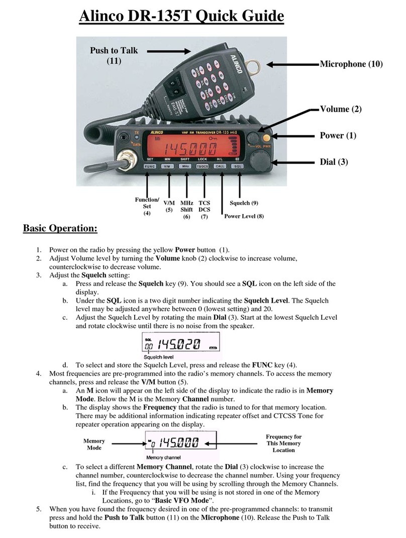
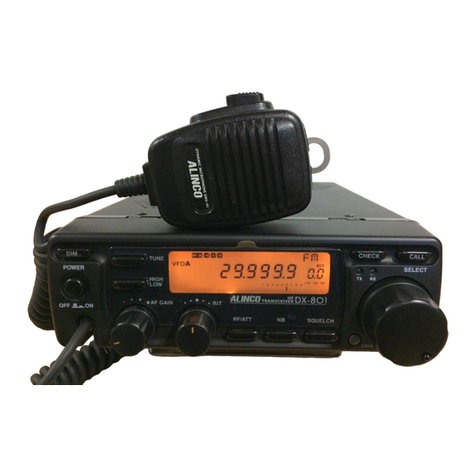
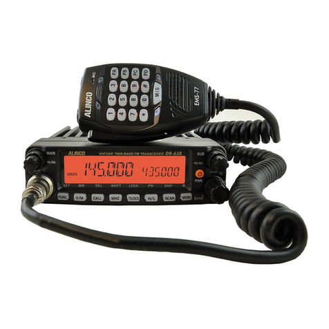
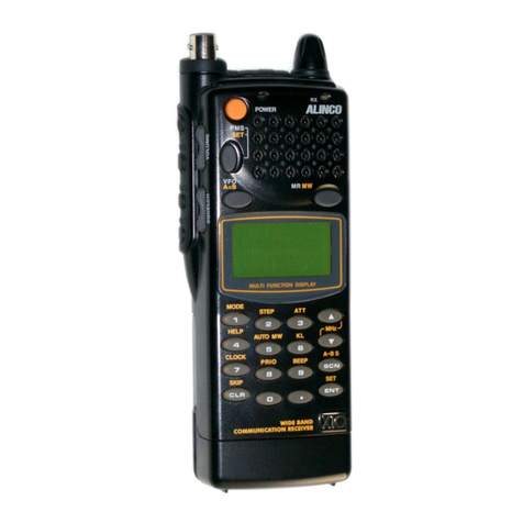
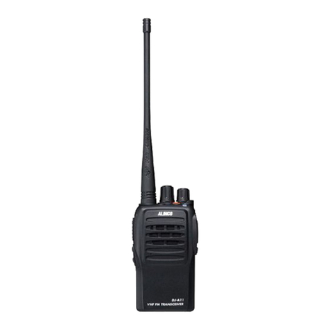
Alinco DX-SR9 T User manual

DX-SR9 T / E
Service Manual
CONTENTS
EXPLODED VIEW
1) Front View....................................................19,20
2) Main Side .....................................................21-23
PARTS LIST
FRONT Unit...........................................................24
LCD Unit................................................................24
PA Unit .............................................................25,26
MAIN Unit.........................................................27-38
Mechanical Unit.....................................................38
Packing Unit ..........................................................38
ADJUSTMENT
1) Required Test Equipment .................................39
2) Adjustment Spot................................................40
3) PA Unit Adjustment...........................................41
4) MAIN Unit Adjustment..................................41,42
5) RX Test Specification........................................43
6) TX Test Specification ...................................44,45
7) Test Specification.........................................45,46
PC BOARD VIEW
FRONT Unit Side A...............................................47
FRONT Unit Side B...............................................48
MAIN Side A..........................................................49
MAIN Side A No.1 .................................................50
MAIN Side A No.2 .................................................51
MAIN Side B..........................................................52
MAIN Side B No.1 .................................................53
MAIN Side B No.2 .................................................54
PA Side A..............................................................55
SCHEMATIC DIAGRAM
FRONT Unit...........................................................56
MAIN Unit (MAIN CPU).........................................57
MAIN Unit (MAIN 1)...............................................58
MAIN Unit (MAIN 2)...............................................59
MAIN Unit (MAIN 3)...............................................60
MAIN Unit (PLL) ....................................................61
MAIN Unit (SDR)...................................................62
PA Unit (PA)..........................................................63
PA Unit (FILTER) ..................................................64
BLOCK DIAGRAM.........................................65
, INC.
SPECIFICATIONS
General....................................................................2
Transmitter ..............................................................2
Receiver ..................................................................2
CIRCUIT DESCRIPTION
1) Receiver System..............................................3,4
2) Transmitter System..........................................5,6
3) Peripheral Circuits............................................7,8
4) PLL Synthesizer Circuits.....................................9
5) R5F2L3ACANFP#U1 (XA1400 / XA1442) ...10-12
SEMICONDUCTOR DATA
1) NJM4558M (XA0097)........................................12
2) BD1754HFN (XA1403)......................................12
3) NJM78M05DL1A (XA1118)...............................12
4) NJM7808FA (XA1106)......................................13
5) TC4S66F (XA0115)...........................................13
6) BU4052BCF (XA0236)......................................13
7) BU4001BF (XA0299) ........................................13
8) TA75S01F (XA0332).........................................13
9) LA4425A (XA0410) ...........................................13
10) TC74HC74AF (XA0459) .................................14
11) NJM3357M (XA0742)......................................14
12) NJM7805FA (XA0812)....................................14
13) UPC2710TB (XA0968)....................................14
14) NJM2594V (XA0995) ......................................14
15) TC74HC390AF (XA1001) ...............................14
16) MB15A01PFV1 (XA1010) ...............................15
17) LM2904PWR (XA1103)...................................15
18) LM2902PWR (XA1106)...................................15
19) S80845CLNB (XA1120) .................................15
20) TC4SU11F (XA1396)......................................15
21) TC74VHC393FT (XA1397) .............................16
22) XC9504B092AR (XA1398)..............................16
23) AD9833BRMA (XA1399).................................16
24) R1EX24256ASAS0A#S0 (XA1401) ................16
25) M61545AFP#DF0R (XA1402).........................17
26) NJM2068V (XA1404) ......................................17
27) TC7WB66FK (XA1407)...................................17
28) LM2904PWR (XA1103)...................................17
29) NJM2783V (XA1525) ......................................17
30) Transistor, Diode and LED Outline Drawing ...18
31) LCD Connection (EL0064)..............................18

2
SPECIFICATIONS
General DX-SR9 T / E
Operating mode J3E (USB, LSB),A3E (AM), A1A (CW), F3E (FM)
Number of memory channels 600 channels simplex
Antenna impedance 50Ωunbalanced
Frequency stability ±1ppm
Power requirement 13.8V DC±15% (11.7 to 15.8V)
Ground method Negative ground
100W
50W
100W 20A (max.)
50W 15A (max.)
Operating temperature -10ºC to 60ºC (+14ºF to +140ºF)
240 (w) x 94 (h) x255 (d) mm (Projections not included)
(9.45’’(w) x 3.7’’(h) x 10’’(d))
240 (w) x 100 (h) x 293 (d) mm
(9.45’’(w) x 3.94’’ (h) x 11.54’’(d))
Weight Approx. 4.1kg (9 pounds)
Transmitter
100W 100W (Hi) Approx.10W (LOW) Approx. 1W (S-LOW)
50W 50W (Hi) Approx.10W (LOW) Approx. 1W (S-LOW)
100W 40W (Hi) Approx. 4W (LOW) Approx. 0.4W (S-LOW)
50W 20W (Hi) Approx. 4W (LOW) Approx. 0.4W (S-LOW)
SSB Balanced modulation
Modulation system
AM Low power modulation
FM Reactance modulation
Spurious emissions Less than -50 dB (Less than -45dB in 30 m band)
Carrier suppression More than 40 dB
Unwanted sideband More than 50dB (1 kHz)
Maximum FM deviation ±2.5 kHz
Receiver
Receiver type Double conversion superheterodyne
SSB (0.15 to 1.8MHz) 0dBu (1uV)
CW ( 1.8 to 30 MHz) -12dBu (10uV)
Sensitivity (0.15 to 1.8MHz) +20dBu (10uV)
( 1.8 to 30 MHz) +6dBu (2uV)
FM ( 28 to 30 MHz) -6dBu (0.5uV)
Intermediate frequency 1st 71.75MHz 2nd 455kHz
CW,SSB (narrow) 1
.0kHz / -6dB 3.0kHz / -60dB
Selectivity
SSB,AM (narrow)
2.4kHz / -6dB 4.5kHz / -60dB
AM, FM 9kHz / -6dB 20 kHz / -50dB
Spurious and image rejection ratio More than 70dB
Audio output power More than 2.0W (8Ω, 10%THD)
RIT variable range ±1.2 kHz
Receive 1.0A (max.) 0.7A (Squelched)
Current drain
Transmit
Dimensions
SSB,CW,FM
Power output
AM
AM
DX-SR9T DX-SR9E
Microphone impedance 300Ω300Ω
160m band (1.8M) 1.80000 - 1.99999MHz 1.80000 - 1.99999MHz
80m band (3.5M) 3.50000 - 3.99999MHz 3.40000 - 3.99999MHz
*60m band (5.3M) 5.25000 - 5.45000MHz -
40m band ( 7 M) 7.00000 - 7.29999MHz 6.90000 - 7.49999MHz
Transmit Frequency 30m band (10M) 10.10000 - 10.14999MHz 9.90000 - 10.49999MHz
coverage 20m band (14M) 14.00000 - 14.34999MHz 13.90000 - 14.49999MHz
17m band (18M) 18.06800 - 18.16799MHz 17.90000 - 18.49999MHz
15m band (21M) 21.00000 - 21.49999MHz 20.90000 - 21.49999MHz
12m band (24M) 24.89000 - 24.98999MHz 24.40000 - 25.09999MHz
10m band (28M) 28.00000 - 29.69999MHz 28.00000 - 29.99999MHz
Receiver Frequency coverage 135kHz - 29.99999MHz 135kHz - 29.99999MHz

3
CIRCUIT DESCRIPTION
SA901 and R903 are installed in the input part of antenna terminal as the
countermeasure against the thunder. The electric charge of antenna is
discharged at R903, and when the voltage becomes over about 300V, the gap
of SA901 is discharged so that the receiving input circuit is protected.
The input signal from antenna is passed through the Tx/Rx selecting relay
(RL903) and passes thru the attenuator of about 20dB (RL906 ON or OFF).
The followings are prevented in LPF consisting of L904, L905, C913, C914,
and C915: 2m band image receiving, passing through the First IF (71.75MHz)
and leaking of the first local oscillating frequency (71.88654~106.75153) to the
antenna terminal.
The receiving signal output from PA Unit is fed to Main unit through CN108.
HPF, consisting of L122, L123, C154, C156, C158, C160, C167, and C168,
eliminates the strong radio signal of MW band of 1.6MHz or below. In case of
receiving the signal of 1.6MHz or below, the received signal is passed through
the low pass Filter (L118, L119, C155, C162, and C163). BPF consists of 8
filters. Each filter covers the following frequency range. The frequency of
2.5MHz or more consists of Chebyshev BPF, and under 2.5MHz frequency
band is LPF.
Range For amateur band
-1.6MHz BPF1
1.6 -2.5MHz BPF2 1.8MHz
2.5 -4.5MHz BPF3 3.5MHz
4.5 -7.5MHz BPF4 7MHz
7.5 -10.5MHz BPF1 10MHz
10.5 -14.5MHz BPF2 14MHz
14.5 -21.5MHz BPF3 18,21MHz
21.5 -30MHz BPF4 24,28MHz
50 -54MHz BPF5 50MHz
Passing through BPF, the signal turns ON/OFF in the switching diode, D120
and D121. This preamplifier is the parallel grounded gate operation of Q128
and Q130 ( 2SK2539 ), so the unit can obtain a good performance at a high
level input signal with low NF.
The wide range frequency from about 1MHz to 60MHz is amplified about 10dB.
This 10dB preamplifier and 20dB attenuator in the PA unit are combined, then
by pressing RF gain switch on the front panel, one of four steps, -20, -10, 0, or
+ 10dB is selected.
The LPF consisting of L146, L147, C235, C236, C252 and C253, prevents the
following first receiving mixer from the local oscillation leaking, and also
prevents the first IF and image of the spurious receiving.
The first receiving mixer consisting of Q128 and Q130 is the balanced mixer, in
which the local oscillating signal is led to the gate of 2SK2539. The 3rd
intercept point is about 20dBm, and local oscillator of about 2V P-P is led to the
gate. The receiving signal is converted into the first IF of 71.75MHz.
1) Receiver System
1. PA Unit
2. Main Unit
a. Front End
XF102 and XF103 are the crystal filters of 71.75MHz. By the combination of
two filters, the unit has the characteristics of the band width of 15kHz or more
3dB and the value of guaranteed attenuation of 70dB or more. Here the image
ratio is determined 70dB or more (approx. 80dB). The first IF amplifier circuit of
Q124 located between the crystal filters to prevent the loss in the front-end and
mutual interference.
The first IF amplifier circuit Q124 decides the sensitivity after passing the
mixer. AGC voltage is applied to the second gate.
DBM (Double Balanced Mixer) consists of L114, D111 and L115. The signal is
passed in the opposite direction while receiving or transmitting in this DBM.
Approximately 0dBm is fed as the second local oscillating level, and the third
IP is approximately 10dBm.
The receiving signal (71.75MHz) and the second local oscillating frequency
(71.295MHz) is mixed, and unwanted signal is eliminated in LPF consisting of
L101, L102 and C119, then the signal of 455kHz is generated. After passing
through the switching diode D108, the signal is amplified in Q110. The source
of Q110 is controlled by the output of the noise blanker circuit.
After passing through the transmission/reception switching diode D110, the
signal is led to one of three ceramic filters of 455kHz. The selectivity is decided
here except CW narrow.
SSB, AM-NARROW FL3(CFJ455K5) 2.4kHz/-6dB 4.5kHz/-60dB
SSB-NARROW, CW FL2(CFJ455KB) 1.0kHz/-6dB 3.0kHz/-60dB
FM, AM FL4(CFW455G) 9kHz/-6dB 20kHz/-50dB
There are two switching diodes for input and output of each filter (D129 to
D150), securing isolation. The isolation required is more than the guaranteed
attenuation for each filter (about 70dB). The filters not used are shorted by
diodes parallel to the filters and cut by the diodes in series, therefore the
combination achieves high level of isolation from the signal. The filter switching
is done by the Q141, Q142, Q143, Q145, D128, D145, D146 and D151, and
the switching configuration depends on the mode, Tx/Rx, and Wide/Narrow
status.
After the filter, passing thru a Tx/Rx switching diode (D128), the signal is
amplified by the Q138 and Q139, and buffered by the Q137. The second gates
of the Q110, Q138 and Q139 are controlled by the AGC circuit. The level of the
received signal for which AGC is applied is of high amplitude and constant at
the output of the Q137.
This output is used for demodulation of SSB, AM, and CW modes besides
used for AGC detection. In the FM mode, the signal having amplified by the
Q138 is partly input to the IC110 (MC3357) thru the C353 and is amplified and
demodulated. The demodulated signal is amplified by an op-amp inside the
IC110. A feedback resistor (R351) has a parallel capacitor (C365) for
de-emphasis. The Q110, Q138 and Q139 are also operational during the FM
mode and the AGC is effected.
b. The First IF Amplifier Circuit
c. The Second Mixer Circuit, The Second Amplifier Circuit
d. IF Filter
e. Second I.F. Amp

4
When in SSB or CW mode, the local oscillation signal mentioned below from
DDS circuit is input to the balanced mixer of the IC104. The received signal is
input to pin No.5, the local signal at 5V p-p to pin No.7. The Q610 is amplifier
that amplifies the local signal to 5V p-p.
Local Osc : USB 456.5kHz + IF SHIFT
LSB 453.5kHz + IF SHIFT
CWU 455.0kHz + (sidetone freq) + IF SHIFT
CWL 455.0kHz - (sidetone freq) + IF SHIFT
The IC4 is an active filter combined of high pass and low pass filters by
op-amps, which has a passband of about 600Hz (-6dB) with its centre at about
800Hz.
The IC107 is an analogue multiplexer with two channels and four contacts,
which switches the demodulated output and AGC time-constant dependent on
mode. The mode voltage is made by combination of the D139 and D140, which
is input to pin No.9 and 10, thereby switching CW audio filter output and
demodulated output of (SSB), FM, and AM. While transmitting, 8V is imposed
to pin No.6 (inhibit) turning the demodulated output off.
The AF signal, after passing thru an analogue switch, is amplified by about
50dB with the IC113:A. The output of pin No.1 of the IC113A is fed to AF Gain
potentiometer for audio output control. The potentiometer output is voltage-
divided with the R383 and R392 and is fed to the IC112, an AF amp. By said
voltage division, input level isadjusted at thesame timethe input impedanceis
lowered for the IC112 therefore residue noise is lowered
The IC112 is an AF power amp, while the Q147 and C393 form ripple filter.
Over 2W output is obtained at 8 ohm load and 10% distortion. This output is
used as the terminal of packet RTTY, SSTV, etc.
The AGC is affecting to one stage in the first IF circuit, and three stages in the
second IF circuit, a total of four stages. Each amplifier stage is made of
3SK293 with AGC on the second gate. The bias on the first gate of 3SK293,
and the source resistor and voltage at the second gate have been determined
their operational level so that the gain is lowered linearly against the voltage
lowering at the second gate. (The source resistor: 470 ohm; the first gate about
3.7). The D144 is for signal detection and the Q140 is for DC amplification. The
anode of the D135 is set at 4.1V by the R321, D135, R280 and R292. Since
little current flows through the IC106C feedback resistor the VR104, input
resistor R290 and D135 to R321, the voltage of AGC line is about 4.2V. When
there is detection voltage on the D144 due to receiver input signal, the Q140
attempts to lower the AGC voltage. When AGC is set FAST in SSB or CW,
there is the C336 between AGC line and the power supply. The raise in
receiver input signal is AGC controlled dependent on the time-constant which
is determined by R326 and C336 hence the transient response is set.
Discharging is determined by the C336 and R290 and the resulting characteris-
tic is of fast-attack/slow delay type.
f. Demodulator
g. CW Audio Filter
h. AF Switching/AGC Time-Constant Switching
i. AF Amplifier
j. AGC
When the AGC is set to SLOW, an analogue switch in the IC108 turns ON and
the R333 and C351 comes in parallel, and R333 with C351 makes discharge
time longer without affecting the attack time.When in AM mode, the C325 is
further added in parallel, which delays the attack time and the AGC response
becomes of average-value type. The D135 are for temperature compensation.
If the received signal delays with a narrow filter before AGC detection followed
by AGC-detection and amplification further delaying for AGC-detection, it
would cause amplifying with more gain and this loop would start hunting
effects. For anti-hunting purpose in this regard, the AGC has more CR
time-constant and slower operation as applicable stage comes closer to the
antenna input. The final stage of I.F. varies its amplification immediately by the
AGC detection voltage resulting in uniform level received signal, dependent on
the transient response. That is, if the received signal suddenly increases, the
received output would first be controlled for uniform output by the I.F. final
stage, then step by step the AGC is applied to earlier stages, finally affecting
the AGC on the final stage to be smaller. For AM reception, there is already
AGC voltage due to carrier, and the AGC is averaged independent of the
modulation level.
TThe output of IC106C is sent to the CPU to display the S-meter. The output
signal of IC106C is fed to pin IC106D. The voltage of pin No.13 of IC106D is
determined by the squelch VR of front unit. Comparing with this voltage, the
squelch is opened or closed. During the check operation the CPU output
decreases the voltage of squelch VR in front side to open the squelch deliber-
ately. The squelch output controls the IC106C, at the same time it is provided
to the front unit to light RX LED.
This circuit eliminates the pulse noise of a car, etc. Because the noise emitting
time is short, in this duration the operation of receiver is stopped to prevent the
unit from emitting a noise. The pulse noise is delayed when it is passed through
the narrow band filter, and the emitting time becomes longer. It makes difficult
to eliminate the noise, so it is necessary to eliminate the noise in the earlier
stage. A part of the second mixer output, whose band width is limited, is
amplified in Q118, Q114, Q115, and Q116. The signal is detected in D115 and
D118, and the AGC voltage is applied to Q115, Q114 and Q116.
The charge time constant of this AGC is determined by R192 and C201, and
also the discharge constant is determined by R191+R192, C201. The voltage
of AGC does not rise suddenly because of the charge constant, so that this
voltage is not applied to almost all the short signals such as pulse noise, but is
applied to the continuous signals such as receiving signal and amplifier gain is
decreased.nal.
k. S-meter, Squelch
l. Noise Blanker

5
The input signal from microphone goes thru mic-gain pot the VR117 and is fed
to a low noise amp the Q180. At the mic terminal there is an 5V bias thru the
R109 for providing voltage to certain type of mics. The IC119A has the gain
(about 20dB) which is determined by the R492 and R512. When in FM mode,
the gain increases by about 35dB due to the R494 parallel to the R512 thru the
Q175, and by the C465 the lower cut-off frequency is increased thereby
activating pre-emphasis and limiter. When in SSB or AM, if the speech
compressor is turned ON, the gain increases by about 35dB due to the C460,
R487, and Q172, and the IC119:A works as a limiter. The C460 cuts off lower
spectrum portion and the audio quality becomes suitable for speech compres-
sion. The in FM, the gain is adequately obtained and there is no effect of
speech compression. If the FM sub-tone is activated, the output of the IC119:A
pin No.1 is voltage divided by the R499 and R509, and the sub-tone fed thru
the R509. The IC119:B is a low pass filter which works as a splatter filter when
in FM and a low pass filter when speech compressor is in use. The output is
either fed to PLL circuit for FM modulating, or to the IC105 for balanced
modulation. The output of the IC105 is muted by the Q178 when in CW or FM.
IC105 is the balanced mixer, and the carrier is suppressed in SSB mode. To
get more ratio or carrier suppression, the balance adjustment of VR102 and
VR103 are applied. The carrier is necessary in CW/FM/AM mode, so the input
of Pin7 is made unbalanced by applying the DC voltage to obtain the carrier.
By applying the DC in AM/FM mode, or by keying in CW mode, the balance is
broken to obtain the carrier wave. VR115 is used for the adjustment or carrier
level in AM/FM mode. VR118 is used for the adjustment of carrier level in CW
mode. In the AM mode, the DC and modulation is added simultaneously. In
SSB mode, the modulation is added by R488. In AM mode, D174 is DC-biased
and turned ON. Then the attenuator consisting of R488 and R443 or R523
limits the modulation.
The output of the IC105 goes thru a temperature compensating thermistor
TH101 and the D128 and is fed to bandwidth limiting I.F. filter. Pulling up
cathode of the D128 when in Tx (and L when in Rx) makes Tx/Rx isolation
better. When in SSB mode, the signal becomes DSB without the carrier.
Switching of the filters is done by the diode switching mentioned before. For
each respective mode, filters are used as follows.
SSB, CW, AM-NARROW FL102 (CFJ455K5) 2.4KHz/-6dB 4.5KHz/-60dB
CW-NARROW FL101 (CFJ455K8) 1.0KHz/-6dB 3.0KHz/-60dB
FM, AM FL103 (CFW455G) 9.0KHz/-6dB 20KHz/-50dB
Having passed the filter, the signal passes thru a switching diode (D110), amp
(Q104), and the D108, and thru the second mixer in reverse direction of Rx,
making 71.75 MHz signal. The Q107 depends on CW keying that improves
isolation when CW key is up. An ALC voltage is applied on the second gate of
the Q104. Signals from 71.295MHz local oscillator and reverse heterodyne are
filtered by the XF102. The signal is amplified by the Q614 and is input to a
balanced mixer. (D111).
2) Transmitter
1. MAIN Unit
a. Mic Amp
b. Balanced Mixer
c. IF filter
d. IF Amp, Second Mixer
The first transmit mixer comprising of the Q103, Q108, L104 and L117 is a
balanced type mixer and input about 3dBm of local oscillator
(71.75MHz+TxFreq) to obtain the wanted frequency. The signal converted to
the wanted frequency by the first Tx mixer is passed thru an LPF to filter out the
local frequency and image components before it is input to the Tx preamp.
The Q105 is a wide band amplifier. It can put out high power with saturating
output of about + 13dBm and more than 20dB gain. Inserting attenuators on
both the input and output make it widen its range with more stability. The output
at the Transmitter First Mixer is about 0dBm when the transmitter power is
100W.
By keying, the Q165 is turned on to the base of the Q162 in the main unit is
pulled to Low which causes the collector to output a voltage. This output
controls all the circuit which operates by CW keying. The output of the Q162
collector goes thru the D180, IC105, VR103, and D126 and by applying a DC
voltage to the balanced mixer it unbalances the mixer and generates a carrier.
VR118 determines the CW waveform of rising edges and falling edges by
adjusting the carrier level in R525 and C488. At the same time, the Q159 is
turned ON to turn OFF the Q107 isolating in keying. The C428 makes the Q107
OFF duration longer than keying duration to avoid effects to the output
waveform. By the D180 a voltage is input to pin No.10 of the IC119:C, and by
the output from pin NO.8 the Q161 is turned ON and the D171 pulling the PTT
line down to Low brings the transmitter ON. The capacitors at the input of pin
No.10 of the IC119:C (C246, C247) determines transmit time delay after stop
of keying. The BK1, BK2, and BK3 are 3 bit break-in time constant voltages
which are combined by the combination of the R469, R470 and R471 as D/A
for obtaining 8 levels of voltage. When all of the BK1, BK2, and BK3 are low,
the status if full-break-in, when more than one of the BK1, BK2, and BK3 have
voltage the status is semi-break-in and the break-in time fastest when all of
them have voltage. When in full-break-in, each of the BK1, BK2, and BK3,
voltages are low hence the Q164 is OFF, making a very fast discharge
time-constant with the C431 alone. When either of several of the BK1, BK2, or
BK3 has voltage, the Q164 would turn ON and the C434 would be added
parallel to the C431 making the time-constant longer which determines the
delay time for semi-break-in. There are 7 levels of semi-break-in voltages out
of the BK1, BK2, and BK3, that is fed to the IC119:C as comparative voltage to
change the discharge time constant. Thus the time constant is the shortest if all
of the BK1, BK2 ,BK3 outputs voltage. When in AUTO-break-in, the output is
from BK1 only, and the comparative voltage for the IC119:C is controlled with
the output voltage of the IC119:D. The keying output when in AUTO mode is
output with each keying using the one-shot multi-vibrator comprising of the
IC120:A and B. Hence the average value of the IC120:A output voltage would
be proportional to average speed of keying. To obtain average voltage, the
R463 and C432, etc. are used for integrating, and the output is DC amplified by
the IC119:D whose output is used as comparative voltage for keying. The
D182 is for turning OFF when in AUTO mode; when AUTO is low, the voltage
charging the C432 is shorted and AUTO is stopped.
e. Transmitter First Mixer
f. Tx Pre AMP
g. CW Keying Circuit
6
The signal input is amplified by the Q803 to about 100mW. By having the idling
current of about 100mA the amplification is A-class. With the feedback the
frequency response is compensated, and with a capacitor parallel to the
emitter resistor the frequency is compensated totally. Then the signal is
amplified to about 5 watt with the Q801 and Q805 (RD16HHF1) where the
idling current is 800mA (adjusted with the VR804) in push-pull configuration.
The D804 and D805 is thermally contacting the Q801 and Q805 to compensate
idling temperature.
There is about 1.6A of idling current in the final amp circuit consisting of the
Q802 and Q804 (RD100HHF1). The D801 and D802 are thermally conducting
with the Q802 and Q804 for temperature compensation. Feedbacks exist thru
the R804 and R822 from collector side averaging the gain in a wide range. The
output of 100W goes to the filter circuit. The collector current of the Q802/Q804
is detected due to the voltage drop caused by resistance of the FB803 and
L801, and is output to the main unit.
The fan is controlled under the temperature of the Q802 and Q804 which is
sensed by a thermistor (TH801). While transmitting, due to temperature rise,
the resistance of the TH801 goes down and voltage of inverted input for the Pin
No.1 of IC101 (MAIN UNIT) goes down. The IC101 (Pin No.1) input is applied
a voltage corresponding to its voltage thus is compared. When the temperature
is over 50 degrees Celsius approximately, the inverted-input voltage would go
down with comparative voltage, and by the comparator output voltage of the
Pin No.74 of IC101, the Q183 is turned ON and the fan starts running.
As a protection for the final power amp, power down circuits detecting SWR
excessive current, and temperature rise have been installed.
2. PA Unit
a. Power Amp
b. Final Power Amp
c. Cooling Fan Control
d. Protection Circuit
The D179 and R457 help to follow speeding up the keying, while the D176 and
R458 determine the discharging time constant in transmission and elongate
the time constant in reception so that it compensates the time constant
recovery during the reception. By doing this, the circuit can follow the keying
speed; transmission can continue between letters; and reception can take
place between words. The circuit is good typically between 30 characters per
minute to 200 characters per minute.
The forward voltage obtained in the PA unit correspondent with transmit power
is input to the IC118:A for invert amplification. At the non-inverting input there
is a voltage, and the output voltage is shifted by the non-inverted input voltage.
There is already about 4.0V on the ALC line which is applied to the second gate
of amplification stage that is under ALC control. When a forward voltage is
applied, the output voltage of the IC118:A goes down, and when becomes
lower than about 3V, the D160 lowers the voltage of the ALC line. The VR112
is for adjusting the Tx output to 100W (High power). The VR119 is for adjusting
the Tx output to 10W (Low power). The VR120 is for adjusting the Tx output to
1W (super Low power). By I is soldering, Q166 turns ON and by having the
VR114 in parallel the voltage is brought down to result in 50W. When in AM,
the R448 comes in parallel to lower the output to 40W. When in Low power, the
LOW line brings the R528 and VR119 in parallel to lower the voltage. When in
super Low power, the slow line brings the R529 and VR120 in parallel to lower
the voltage. The Q158 and VR113 are for making the (antenna matcher) TUNE
output to 10W output. Necessary output, however, may be different depending
on the automatic tuner. When the SWR is high, reflected voltage turns on the
Q158 lowering the power. The Q158 is activated from SWR 3 approximately.
The voltage difference detected in the PA unit by the final collector current us
differentially amplified by the IC118:B. The output voltage lowers as current
increases and at some point the ALC line is pulled down thru the D160 lowering
the output power. The operating point is determined by the VR110.
The forward voltage is amplified by the IC118:D for driving the meter. The
D164, R433 and C419 are for instant peak-holding to show the meter more
visible. The D163 and D136 switch to S-meter. The ALC voltage is invert
amplified by the IC118:C. The output voltage is divided from 8V thereby
lowering the feedback resistance so that tolerance caused by bias-leakage is
minimized; further this feedback resistor lets some current to the R423 to
obtain 4.0V to the ALC line. The output is fed to the base of the Q150, leading
to the front unit tell the CPU to switch Tx and Rx besides illuminating the Tx
LED.
h. Power Control/ALC Circuit
i. Overcurrent Protection
j. RF meter circuit, ALC indication

7
5. Low Pass Filter
6. Power Detection Circuit
7. Power Switch
The output from the final power amp goes through the low pass filter removing
the harmonics. The input/output for this filter is switched with a relay, and the
filters not used are shorted to ground thru relays. The LPF control utilizes the
control voltage for the BPF in the main unit. Each LPF is made of 5 pole Cheby-
shev filters, attenuating the second and higher order harmonics by more than
40dB.
L0 ~2.5MHz BPF0, BPF1 1.8MHz band
L1 2.5MHz~4.0MHz BPF2 3.5MHz band
L2 4.0MHz~7.5MHz BPF3 7MHz band
L3 7.5MHz~14.5MHz BPF4, BPF5 10,14MHz band
L4 14.5MHz~21.5MHz BPF6 18,21MHz band
L5 21.5MHz~30.0MHz BPF7 24,28MHz band
The transmitting signal, having removed spurious contents by the LPF goes
thru the power detection circuit and
Tx/Rx switching relay.
The L901 is made by bifilar winding on a toroidal core in 10 turns. Hence the
two sides will have 20 turns with a center tap. When the jumper wire goes thru
the hole of the core, this itself is considered one turn having 1:20 transformer.
Since there are the R902 and R904 in parallel, it effectively means 50 ohm load
existing on both ends. For the jumper wire, it is equivalent to having 50Ω/
(20*20)=0.125Ωresistor existing in series. Hence when outputting 100W, the
voltage applied to ends of the said quasi-resistor is:
0.125/(50+0.125)* (100*50) =0.176V
Since the turn ratio is 20:1, the voltage between the L901 is [0.176*20=3.52V]
The center tap of the coil has the voltage a half of the above therefore the
current will flow reversely to that in the jumper wire. A voltage divided by the
TC901 and C904 is applied to the center tap, the voltage being in phase with
that in the jumper wire. If the voltage is adjusted with the TC901 to be equal to
the enter tap voltage, the R908 would have the voltages in phase adding each
other, and the R909 would have inverted phase canceling each other. If the
antenna impedance changes, there would be a differential voltage on the R909
without having cancellation due to phase or voltage difference hence having a
DC voltage after passing thru the D902. In this way, the voltage applied on the
R913 is proportional to the output power (forward voltage) and on the R914 is
to the reflected power (reflected voltage). Thus the output and reflected powers
are detected and in the main unit the power is controlled.
Pressing the SW1 turns the RL801 contact ON and 13.8V is supplied. At the
same time, the Q101 is turned onand 5V is supplied.
Sidetone is output by the STON line at pin No.24 of the CPU (MAIM UNIT) in
square wave. Beep is output by the beep line at pin No.16 of the CPU (MAIN
UNIT) in square wave. The sidetone frequency is switchable in the range of
400Hz to 1kHz. The VR1 is the volume control put which leads to the AP amp.
At the start of the tuning, the TUNE voltage comes out by which the one-shot
multi-vibrator operates and by the Q168 approximately 8V is output to
command the external auto tuner as a starting signal. Separately, an output
which goes low while tuning is created by the Q169 using the TUNE voltage.
When the starting signal is received by the external auto tuner (e.g. EDX-2),
the tuner outputs the said (low) output at TKEY terminal. The radio’s CPU
monitors the TKEY terminal and while the voltage is at low level the radio is put
to the TUNE mode. If the TKEY terminal is low for more than 20 seconds, the
CPU releases the TUNE mode. During the TUNE mode the radio transmits in
AM mode besides microphone is muted and the carrier is suppressed at 10W
(adjustable).
The IC115 is a regulated power supply of 8V output. The voltage necessary for
transmission, namely T8V is created by the Q149, and for reception R8V by the
Q152. The IC117, Q151 and Q155 are Tx/Rx control. When PTT line is
grounded at the output of the Q161 by mic’s PTT or CW keying, a High level is
output from the IC117:C, and buffered by the Q150 the output is sent to the
CPU in the front unit for Tx/Rx switching. The IC117:C, having delayed the
rising of reception with the R413, C408, and D158, controls Q149 with Q151.
When transmitting, the current flows from 13.8V thru the R410 and D156, and
since the Q149’s base voltage is higher by one diode difference than 8V, the
emitter output will be just 8V. When transmitting, the Q151 is turned ON thus
the Q149’s base voltage will be 0V, resulting no output on T8V line. When
receiving, the T8V line is shorted by the D157 to discharge remaining charges
in the capacitors on T8V line. The Q152 while receiving, similarly as T8V line,
has currents coming thru the D167 and R432 from the 13.8V line, and since the
base voltage of the Q152 is higher by one diode voltage than 8V, the base
voltage of the Q152 will be 0V hence no output on R8V line. When transmitting,
the R8V line is shorted by the D168 to discharge remaining charges in the
capacitors on R8V line. The input to the IC117:D, which goes low when
reception is started, is delayed with the R421 and C412, then inverted by the
IC117:B, followed by the Q155 to control R8V. If a voltage is applied to pin No.8
of IC117:C, the output at pin No.10 would vary with PTT going Low, hence a
PTT Lock is activated.
The CPU (MAIN UNIT) is controlling the mode voltage, preamp On/Off, Attenu-
ator, Power, BPF/LPF switching, AGC, break-in, and PTT-Lock. For each
mode, the Q167, Q170, Q171, Q177, Q179, Q181 and Q182 are turned on
providing 8V.
3) Peripheral Circuits
1. Beep and Sidetone Circuit
2. Tune Circuit
3. Regulated Power Supply
4. Mode Voltage Functions Control, BPF/LPF Switching

8
The IC102, resetting IC for resetting the CPU, turns on and off at 4.5V. When
OFF (0V) the CPU resets. Then the IC1004’s reset signal goes Low and the
CPU stops. The IC116 is the power supply for the CPU, which is made
separate in order for the voltage to sustain 5V until the data is written to the
EEPROM and resetting signal is input.
A regulated power supply of 8V is made of the IC115. The voltage of 8V is
supplied to D3, D4, D5 and D6. The CPU’s EN output is a pulse, which current
value from D3 to D6 is set. When the illumination is at the highest intensity, the
EN output is constant at 5V.
The CPU turns ON the LCD via segment and common terminals with 1/4 the
duty and 1/3 the bias, at the frame frequency of 125Hz.
The CPU (IC101) is equipped with an internal tone encoder. The tone signal
(67.0 to 250.3Hz) is output from pin 45 of CPU. The output of the CPU leading
to the mic amp LPF having mixed with audio signal. The tone is output only
when in FM mode.
The CPU (IC101) is activated by input to pin No.68 for dots, and pin No.69 for
dash. When ElecKey is ON, the electronic keyer in ON, and when Eleckey is
OFF the keying is of semi-automatic (the “bug key”) operation.
The pin 58 of CPU is clone data transmission, and the pin 57 of CPU is
receiving data. Each data is of one line, and input/output is done thru JK2 on
the front unit.
The X1 is a ceramic resonator of 8MHz carefully chosen on its harmonics not
interfering on amateur bands. For the front panel switches, the Y0, Y1, Y2 and
Y3 with regard to the DB0~DB5 are monitored to determine which key is
pressed. On the terminals of RIT and IF-Shift pots, 5V is applied and the
voltage at the input of A/D determines the positions of these pots. The Q1 is for
transmit detection whose output from the main unit and illuminating the Tx
LED. For this reason it cannot be directly input to the CPU therefore the change
is only either on or off. The Q2 is the squelch output from the main unit which
illuminates the Rx LED.
8. Power Supply and Resetting
9. Dimmer
10. LCD
11. Tone
12. Electronic Keye
13. Cloning
14. Miscellaneous
In SDR receiving, 26th pin(SDR) of CPU (IC101) becomes H. Through the
analog switch IC1014 , the received signal of 455KHz, which is amplified by
Q110 then amplified again by Q1002.
On the other hand, BFO (1.82MHz) signal generated by IC604 is divided into
1/4 and in-phase and quadrature signals of 455KHz. This standard signal and
receiving signal amplified by Q1002 are mixed at IC1003 and output as I/Q
signal to JK1003.
In SDR transmitting, the 27th pin(SDT) of the CPU (IC101) becomes H. The I/Q
mixture signal with ±12KHzcarrier frequencies input through the center
terminal of JK1004 goes through IC1017 internal amp circuit and IC1004 buffer
amp. This signal is mixed with a signal of 467KHz came from BFO in a mixer
circuit of Q1016, then finally output as IF signal of 455KHz.
Such 455KHz signal will be output through the same circuit and transmitted
through the 455KHz IF filter of each modes. In SDR operation, when the mode
is changed, the CPU generates appropriate mode signal accordingly.
After amplification in IC123 operational amplifier, the signal from the
microphone is rectified to a DC voltage at D1007, D191.
The rectified voltage that is applied to the CPU 81 pin analog input, transmits
with microphone sensitivity determined by the voltage value.
The data signal input through the center terminal of JK1004 is amplified by
IC1018 then goes through the IC1007 and IC119 microphone amp, passes the
same modulation line as a voice signal and transmitted as a PSK signal.
To transmit, the data signal is rectified by D1002 and D1004, then the rectified
signal toggles Q1011 and inputs L to the 77th pin of the CPU
15. SDR Mode
16. VOX Circuit
17. DATA VOX circuit

9
The reference oscillation frequency for the PLL of the second local oscillator
reference and DDS clock, etc. is set at 16.777216MHz. The signal is oscillated
by the X601, Q609, and Q611 buffered with the Q608. It is used for the DDS
clock for BFO oscillation. It is further divided 1/2064 with the IC606 to
8.128496KHz for the second local oscillator PLL (IC606) reference frequency.
The Q605 is a Hartley oscillator with the Q605 gate grounded which works as
VCO with the oscillation frequency range of 71.75 to 106.75MHz. The Q601
eliminates ripples for stabilizing the power supply, while the Q604 is a buffer
circuit. The output is divided 1/8 with the IC610 and divided 1/5 with the IC611,
hence 1/4 of the first local oscillator frequency (about 1.8 to 2.5MHz) is input to
the phase comparator IC607. Meanwhile the DDS in the IC603 can output in
0.25Hz step, and with a D/A converter of 10bit and LPF, a sinusoidal wave that
is 1/40 of the first local frequency can be obtained. This output, with the phase
comparator will control the signal. The oscillator output frequency will be 10Hz
patch (0.25*40), The IC607 output goes thru a loop filter which is made of high
response, low noise op-amp inside the IC601A; controlling the D602, the
oscillation frequency is controlled. To widen the lock range, some voltages are
supplied to cathodes of the D602. The locking voltage applicable to the anode
of the D602 is in a wide range of 2V to +6V. The IC602 and the Q603 are the
necessary negative voltage, and about -6.5V is attained.
The reference oscillation frequency input to the IC606 is 8.388608MHz which
is divided 1/2064 inside, and the comparison frequency is about 8.128496KHz.
The Q615 is a VCO with 71.295 MHz which is buffered with Q616. The output
is amplified by the amplifier Q620, and dividing it 1/8771 in the IC606, it is fed
to a phase comparator and thru a loop filter, the oscillation frequency is output,
controlled by the D605. Also, this output is amplified by the amplifier Q614 and
fed to the second mixer circuit. When transmitting FM, the anode of the D605
will be superimposed by the modulating signal from the microphone, modulat-
ing into FM signal. When in FM mode, the C697 is added to a loop filter by the
Q618, having the time constant larger and the control under the modulation is
unable, a modulated signal is created thru the VCO. The IC605 is an analog
switch which enables frequency modulation on the VCO only when in FM
mode.
When in SSB or CW, by varying the first local and BFO interlocked, it is
possible to change the relative receiving bandwidth without changing the
receiving frequency. The range for the I.F. shifting for DX-SR8 is +/-1.5kHz in
50Hz pitch.
4) PLL Synthesizer circuits
1. Reference frequency oscillator circuit
2. First Local Oscillator
3. Second Local Oscillator
4. I.F. Shifting (∆IF)

10
5) R5F2L3ACANFP#U1 (XA1400 / XA1442)
FRONT / MAIN CPU
Terminal Connection
(TOP VIEW)
76
P1_6/SEG14 77
P1_5/SEG13 78
P1_4/SEG12 79
P1_3/SEG11/AN15 80
P1_2/SEG10/AN14 81
P1_1/SEG9/AN13 82
P1_0/SEG8/AN12 83
P0_7/SEG7/AN11 84
P0_6/SEG6/AN10 85
P0_5/SEG5/AN9 86
P0_4/SEG4/AN8 87
P0_3/SEG3/AN7 88
P0_2/SEG2/AN6 89
P0_1/SEG1/AN5 90
P0_0/SEG0/AN4 91
VL1 92
VL2 93
VL3 94
CL2/P12_3 95
CL1/P12_2 96
VL4 97
P13_7/AN19/TRGCLKB 98
P13_6/AN18/TRGIOB 99
P13_5/AN17/TRGCLKA 100
P13_4/AN16/TRGIOA
50 P5_0/SEG40
49 P5_1/SEG41
48 P5_2/SEG42
47 P5_3/SEG43
46 P6_0/SEG44/TRDIOA0/TRDCLK
45 P6_1/SEG45/TRDIOB0
44 P6_2/SEG46/TRDIOC0
43 P6_3/SEG47/TRDIOD0
42 P6_4/SEG48/TRDIOA1
41 P6_5/SEG49/TRDIOB1
40 P6_6/SEG50/TRDIOC1
39 P6_7/SEG51/TRDIOD1
38 P7_0/SEG52/COM7
37 P7_1/SEG53/COM6
36 P7_2/SEG54/COM5
35 P7_3/SEG55/COM4
34 P7_4/COM3
33 P7_5/COM2
32 P7_6/COM1
31 P7_7/COM0
30 P10_0/(TRDIOA0/TRDCLK/KI0)
29 P10_1/(TRDIOB0/KI1)
28 P10_2/(TRDIOC0/KI2)
27 P10_3/(TRDIOD0/KI3)
26 P10_4/(TRDIOA1/KI4)
25
P10_5/(TRDIOB1/KI5)
24
P10_6/(TRDIOC1/KI6)
23
P10_7/(TRDIOD1/KI7)
22
P11_0/SCL/SSCK/(CLK2/INT0)/IVREF1/LVCOUT1
21
P11_1/SSI/(RXD2/SCL2/TXD2/SDA2/INT1)/IVCMP1/LVCOUT2
20
P11_2/SDA/SSO/(RXD2/SCL2/TXD2/SDA2/INT2)/IVREF3
19
P11_3/SCS/(CTS2/RTS2/INT3)/IVCMP3
18
P11_4/TRAIO/(INT4/RXD0)
17
P11_5/TRAO/(INT5)
16
P11_6/TRBO/(INT6)
15
P11_7/TREO/(INT7/ADTRG)
14
VCC/AVCC
13
P12_0/XIN
12
VSS/AVSS
11
P12_1/XOUT
10
RESET
9
XCOUT
8
XCIN
7
MOVE
6
VREF
5
WKUP0
4
P13_0/AN0/DA0/WKUP1
3
P13_1/AN1/DA1/TXD0/LVREF
1
P13_3/AN3/CLK0/LVCMP2
2
P13_2/AN2/RXD0/LVCMP1
75
P1_7/SEG15
74
P2_0/SEG16/KI0
73
P2_1/SEG17/KI1
72
P2_2/SEG18/KI2
71
P2_3/SEG19/KI3
70
P2_4/SEG20/KI4
69
P2_5/SEG21/KI5
68
P2_6/SEG22/KI6
67
P2_7/SEG23/KI7
66
P3_0/SEG24/INT0
65
P3_1/SEG25/INT1
64
P3_2/SEG26/INT2
63
P3_3/SEG27/INT3
62
P3_4/SEG28/INT4
61
P3_5/SEG29/INT5
60
P3_6/SEG30/INT6
59
P3_7/SEG31/INT7/ADTRG/TRCTRG
58
P4_0/SEG32/TXD1
57
P4_1/SEG33/RXD1
56
P4_2/SEG34/CLK1
55
P4_3/SEG35/TRCCLK/TRCTRG
54
P4_4/SEG36/TRCIOA/TRCTRG
53
P4_5/SEG37/TRCIOB
52
P4_6/SEG38/TRCIOC/TRCIOB
51
P4_7/SEG39/TRCIOD/TRCIOB
FRONT CPU (XA1400)
No. Terminal Signal I/O Description
1 P13 UP I UP Key input
2 P13/RXD0 RXD I UART data reception input
3 P13/TXD0 TXD O UART data transmission output
4 P13 -
5WKUP GND -GND
6VREF 5V -5V
7MODE 5V -5V
8XCIN -
9XCOUT -
10 RESET RESET I Reset input
11 XOUT XOUT O Main clock output
12 VSS GND - CPU GND
13 XIN XIN I Main clock input
14 VCC 5V - CPU power terminal
15 P11 EN O LCD Dimmer
16 INT6 PTT I PTT input
17 P11 DOWN I DOWN Key input
18 INT4 DIAL1 I
19 INT3 DIAL2 I
20 P11 Y0 O
21 P11 Y1 O
22 P11 Y2 O
23 P11 Y3 O
24 KI6 DB0 I
25 KI5 DB1 I
26 KI4 DB2 I
27 KI3 DB3 I
28 KI2 DB4 I
29 KI1 DB5 I
30 P10 MUTE O Microphone mute
31 COM0 COM0 O LCD COM0 output
32 COM1 COM1 O LCD COM1 output
33 COM2 COM2 O LCD COM2 output
34 COM3 COM3 O LCD COM3 output
35 SEG55 SEG55 O
36 SEG54 SEG54 O
37 SEG53 SEG53 O
38 SEG52 SEG52 O
39 SEG51 SEG51 O
40 SEG50 SEG50 O
41 SEG49 SEG49 O
42 SEG48 SEG48 O
43 SEG47 SEG47 O
44 SEG46 SEG46 O
45 SEG45 SEG45 O
46 SEG44 SEG44 O
47 SEG43 SEG43 O
48 SEG42 SEG42 O
49 SEG41 SEG41 O
50 SEG40 SEG40 O
51 SEG39 SEG39 O
52 SEG38 SEG38 O
53 SEG37 SEG37 O
54 SEG36 SEG36 O
55 SEG35 SEG35 O
56 SEG34 SEG34 O
LCD segment signal
Rotary encoder input
Key matrix input
Key matrix input

11
FRONT CPU (XA1400)
No. Terminal Signal I/O Description
57 SEG33 SEG33 O
58 SEG32 SEG32 O
59 SEG31 SEG31 O
60 SEG30 SEG30 O
61 SEG29 SEG29 O
62 SEG28 SEG28 O
63 SEG27 SEG27 O
64 SEG26 SEG26 O
65 SEG25 SEG25 O
66 SEG24 SEG24 O
67 SEG23 SEG23 O
68 SEG22 SEG22 O
69 SEG21 SEG21 O
70 SEG20 SEG20 O
71 SEG19 SEG19 O
72 SEG18 SEG18 O
73 SEG17 SEG17 O
74 SEG16 SEG16 O
75 SEG15 SEG15 O
76 SEG14 SEG14 O
77 SEG13 SEG13 O
78 SEG12 SEG12 O
79 SEG11 SEG11 O
80 SEG10 SEG10 O
81 SEG9 SEG9 O
82 SEG8 SEG8 O
83 SEG7 SEG7 O
84 SEG6 SEG6 O
85 SEG5 SEG5 O
86 SEG4 SEG4 O
87 SEG3 SEG3 O
88 SEG2 SEG2 O
89 SEG1 SEG1 O
90 SEG0 SEG0 O
91 VL1 VL1 -
92 VL2 VL2 -
93 VL3 VL3 -
94 P12 RXLED O RX Lamp
95 P12 TXLED O TX Lamp
96 VL4 VL4 - LCD power supply
97 AN19 VOL I Volume input
98 AN18 SQL I SQL Volume input
99 AN17 SHIFT I SHIFT Volume input
100 AN16 RIT I RIT Volume input
LCD segment signal
LCD power supply
No. Terminal Signal I/O Description
1 P13/AN3 TEMP I Temperature detection of transmission AMP
2 P13/RXD0 RXD I UART data reception input
3 P13/TXD0 TXD O UART data transmission output
4 P13/DA0 SQV O Output of voltage for squelch
5 WKUP0 GND - GND
6VREF5V -5V
7MODE5V -5V
8XCIN - -
9XCOUT - -
10 RESET RESET I Reset input
11 XOUT XOUT O Main clock output
12 VSS GND - CPU GND
13 XIN XIN I Main clock input
14 VCC 5V - CPU power terminal
15 P11 BU I Backup signal detection input
16 TRBO BEEP O Beep tone output
17 INT5 ULK I PLL unlock signal input
18 P11 5VC O 5V power ON/OFF output
19 P11 O -
20 SDA EDAT I/O Serial data for EEPROM
21 SCL2 CLK O Serial clock output for PLL
22 SCL ECLK O Serial clock output for EEPROM
23 P10 DAT O Serial data output for PLL
24 TRDIOC1 STON O Side Tone Output
25 P10 STB O Strobe signal output for PLL
26 P10 O
27 P10 O
28 P10 O -
SDR
SDT
29 P10 PSW I Power switch input
30 P10 PON O Unit power ON/OFF
31 P7 USB O USB mode setting
32 P7 LSB O LSB mode setting
33 P7 CWU O CWU mode setting
34 P7 CWL O CWL mode setting
35 P7 AM O AM mode setting
36 P7 FM O FM mode setting
37 P7 TUN O Output of Voltage for antenna tuner
38 P7 NRW O Narrow mode setting
39 P6 NBS O Noise Brounker setting
40 P6 AGCS O AGC setting
41 P6 LOW O Tx power LOW
42 P6 SLOW O Tx power SLOW
43 P6 MUTE O Microphone mute
44 TRDIOCO - -
45 TRDIOBO TONE O CTCSS tone output
46 TRDIOAO - -
47 P5 ATT O Attenuator ON/OFF
48 P5 BK1 O
49 P5 BK2 O
50 P5 BK3 O
51 P4 AUTO O
52 P4 PTT O PTT Output
53 P4 PTTL O PTT Lock
54 P4 50W O Tx Power 50W
55 P4 VDAT O EVR control data output
56 CLK1 VCLK O Clock output for EVR
Break-in
MAIN CPU (XA1442)
SDR receive mode signal
SDR transmission mode signal

12
No. Terminal Signal I/O Description
57 RXD1 CRX I Clone data reception input
58 TXD1 CTX O Clone data transmission output
59 P3 BPF0 O 1.6MHz BAND
60 P3 BPF1 O 1.9MHz BAND
61 P3 BPF2 O 3.5MHz BAND
62 P3 BPF3 O 7MHz BAND
63 P3 BPF4 O 10MHz BAND
64 P3 BPF5 O 14MHz BAND, 18MHz BAND
65 P3 BPF6 O 21MHz BAND, 24MHz BAND
66 P3 BPF7 O 28MHz BAND, 29MHz BAND
67 P2 PRE O PRE AMP ON/OFF
68 P2 DOT I CW DOT input
69 P2 DASH I CW DASH input
70 P2 CWK O Transmission control in CW mode
71 P2 TXS I Detection of transmission
72 P2 SQS I squelch Open/Close
73 P2 50I I Tx Power 50W setting
74 P2 FAN O Fan Motor control
75 P1 TKEY I Detection of Antenna tuner operation
76 P1 COMP O
77 P1
78 P1 PTTD
DVOX O
IPTT detection of DVOX mode
DVOX mode setting
79 AN15 SRF I S-meter input/RF meter input
80 P1
81 P1
82 P1 - -
ALC
VDET I
IALC voltage input
VOX voltage input
83 P0 JP1 I Band plan 1
84 P0 JP2 I Band plan 2
85 P0 JP3 I Band plan 3
86 P0 JP4 I Band plan 4
87 P0 JP5 I Band plan 5
88 P0 JP6 I Band plan 6
89 P0 JP7 I Band plan 7
90 P0 JP8 I Band plan 8
91 VL1 - -
92 VL2 - -
93 VL3 - -
94 P12 - -
95 P12 - -
96 VL4 - -
97 P13 SCLK O Serial clock output for DDS
98 P13 SDAT O Serial data output for DDS
99 P13 FSY1 O 1st LO data for DDS
100 P13 FSYB O BFO data for DDS
MAIN CPU (XA1442)
123
1.INPUT
2.GND
3.OUTPUT
14
85
B1D
745
SEMICONDUCTOR DATA
1) NJM4558M (XA0097)
Operation Amplifiers
2) BD1754HFN (XA1403)
LED Driver Series
3) NJM78M05DL1A (XA1118)
5V Voltage Regulator
PIN
1
2
3
4
5
6
7
8
Pin Name
EN
GND
ISET
VIN
L1
L2
L3
L4
GND
ISET
VIN
EN UPIC
6
L1 L2 L3 L4
Current
DAC

13
4) NJM7808FA (XA1106)
8V Voltage Regulator
6) BU4052BCF (XA0236)
Analog Switch
5) TC4S66F (XA0115)
Bilateral Switch
1. OUTPUT
Pin Assignment
2. COMMON
3. INPUT
123
C9
VDD
CONT
IN/OUT
VSS
5
4
1
OUT/IN 2
3
BU4052BCF
14 8
1 7
VDD
VSS
VEE
X0
X1
X2
X3
Y0
Y1
Y2
Y3
INHIBIT
A
B
LEVEL
CONVERTER BINARY TO 1 of 4 DECODER
WITH INHIBIT
COMMON
X
COMMON
Y
Y0 1
Y2 2
COMMON Y 3
Y3 4
Y1 5
INHIBIT 6
VEE 7
VSS 8
VDD16
X215
X114
COMMON X13
X012
X311
A10
B9
DV
B
2Y
Y OUT/IN
3Y
1Y
INH
VEE
2X
1X
OUT/IN X
0X
3X
A
7) BU4001BF (XA0299)
Quad 2-input NOR GATE
8) TA75S01F (XA0332)
Single Operational Amplifiers
9) LA4425A (XA0410)
5W Audio Power Amplifiers
S A
5
12
4
3
5
VCC
IN(+) IN(-)VEE
OUT
12
4
3
+
4O2
5B2
6A2
7VSS
14 VDD
13 A4
12 B4
11 O4
10 O3
9B3
8A3
1A1
2B1
3O1
1 2 3
LA4425
45
Vcc=13.2V RL=4ΩPo-5W Gain=45dB
Input 1
23
5
4
2.2μF
Vcc
SP
13.2V
+
Test Circuit
1000μF
+
1000μF
+4Ω

14
1. OUTPUT
2. COMMON
3. INPUT
123
10) TC74HC74AF (XA0459)
Dual D-type Flip Flop
11) NJM3357M (XA0742)
Low Powe FM IC
12) NJM7805FA (XA0812)
5V Voltage Regulator
Pin Assignment
1CLR 1
1D 2
1CK 3
1PR 4
1Q 5
1Q 6
GND 7
14 VCC
13 2CLR
12 2D
11 2CK
10 2PR
9 2Q
8 2Q
QQ
CK D
QQ
CK D
1
Oscillator
Mixer
Squelch Trigger
with Hysteresis
Limiter Amp
Demodulator
Active
Filter
Amp
2
3
4
5
6
7
8
16
15
14
13
12
11
2V 10
9
13) UPC2710TB (XA0968)
Wide Band Amp
14) NJM2594V (XA0995)
Balanced Mixer
15) TC74HC390AF (XA1001)
CMOS Dual Decade Counter
PIN
1
2
3
4
5
6
Pin Name
INPUT
GND
GND
OUTPUT
GND
VCC
2
1
3
5
6
4
C1F
1CKA 1
1CLR 2
1QA 3
1CKB 4
1QB 5
1QC 6
1QD 7
GND 8
16 VCC
15 2CKA
14 2CLR
13 2QA
12 2CKB
11 2QB
10 2QC
9 2QD
8
NC 7 6 5
1 2
OUTPUT1
3
OUTPUT2
4
GND
CARRIER
INPUT BYPASS SIGNAL
INPUT
CKA QA
1.15 BINARY
COUNTER
QUINARY
COUNTER
3.13
CLR 2.14
CKB QC
4.12 6.10
QD
7.9
QB
3.13
VCC=16, GND=8

15
16) MB15A01PFV1 (XA1010)
PLL Synthesizer
17) LM2904PWR (XA1103)
Dual Operational Amplifiers
1. OSC IN
2. OSC OUT
3. Vp
4. Vcc
5. Do
6. GND
7. LD
8. fin
9. Clock
10. Data
11. LE
12. FC
13. N. C.
14. fout
15.φP
16.φR
Control Circuit
MC
fp
910111213141516
87654321
***
15A01
****
VCC
GND
Clock
Data
LE
fin
OSC IN
OSC OUT
Control
1bitlatch
Oscillator
Crystal
DATA
SW
LE
Prescaler
64/64
128/129
Binaly7-bit
counter
swallo programmable
Binary11-bit
counter
Programmabledivider
18-bitlatch
11-bitlatch7-bitlatch
19-bitshiftregister
15-bitlatch
15-bitlatch
19-bitshiftregister
SW
LE
fr
fp
Programmablereferencedivider
referencecounter
Binary14-bit
Chargepump
detector
Digitallock
Phase
comparator
LD
fout
FC
φR
φP
Do
Vp
frequency
switching
Monitor
circuit
fp
fr
LD
FC
18) LM2902PWR (XA1106)
Quad Operational Amplifiers
19) S80845CLNB (XA1120)
C-MOS Voltage Detector
20) TC4SU11F (XA1396)
2 Input NAND GATE
34
21
Pin No.
1
2
3
4
Voltage detection output pin
Voltage input pin
No connection
GND pin
OUT
VDD
NC*1
VSS
Pin name Pin description
*1. The NC pin is electrically open.
The NC pin can be connected to VDD or VSS.
C7 VDD
OUT X
IN B
GND
5
4
1
IN A 2
3

16
1 1CK
2 1CLR
3 1QA
4 1QB
5 1QC
6 1QD
7 GND
8 2QD
9 2QC
10 2QB
11 2QA
12 2CLR
13 2CK
14 VCC
21) TC74VHC393FT (XA1397)
Dual Binary Counter
22) XC9504B092AR (XA1398)
2ch. Step-up/Inverting DC/DC Converter
PIN No.
1
2
3
4
5
6
7
8
9
10
Pin Name
EXT1
VDD
FB1
PWM1
EN1
EN2
PWM2
FB2
GND
EXT2
FUNCTION
External Transistor Connection 1
Supply Voltage
Output Voltage Monitor Feedback Pin 1
PWM / PFM Switching Pin 1
Enable 1
Enable 2
PWM / PFM Switching Pin 2
Output Voltage Monitor Feedback Pin 2
Ground
External Transistor Connection 2
CLR
1/13
2/12
CK
3/11QA
R
D
CK Q
4/10QB
R
D
CK Q
5/9QC
R
D
CK Q
6/8QD
R
D
CK Q
1B0
92xx
1pin
EXT1
VDD
FB1
PWM1
EN1
EXT2/
GND
FB2
PWM2
EN2
Vref2=0.9V
EN2
OSC
Generator
PWM/PFM
Controller2
PWM
Comparator2
EN2 to
internal circuit
Error Amp2
Ramp Wave
Generator2
Vref1=0.9V
with Soft Start1.
EN1
PWM/PFM
Controller1
PWM
Comparator1
EN1 to
internal circuit
Error Amp1 Ramp Wave
Generator1
23) AD9833BRMZ (XA1399)
Programmable Waveform Generator
24) R1EX24256ASAS0A#S0 (XA1401)
256K bits CMOS Serial EEPROM
A0
A1
A2
GND
1
2
3
4
VCC
WP
SCL
SDA
8
7
6
5
Pin
Number
1
2
3
4
5
6
7
8
Pin
Name Function
A0
A1
A2
GND
SDA
SCL
WP
VCC
Slave address input
Slave address input
Slave address input
Groudd
Serial data input / output
Serial clock input
Write protection input
Connected to Vcc: Protection valid
Connected to GND: Protection invalid
Power supply
Remark See Dimensions for details of the package drawings.
AD9833
COMP 1 VOUT10
VDD 2 AGND9
CAP/2.5V 3 FSYNC8
DGND 4 SCLK7
MCLK 5 SDATA6
MCLK
AGND DGND VDD
AVDD/
DVDD 2.5V
CAP/2.5V
REGULATOR
FULL-SCALE
CONTROL
ON-BOARD
AEFERENCE
MUX
PHASE0 REG
PHASE1 REG
MUX
MUX
10-BITDAC
PHASE
ACCUMULATOR
(28-BIT)
12
∑SIN
ROM
COMP
VOUT
R
200Ω
MUX
DIVIDE
BY 2
MSB
FREQ0 REG
CONTROL REGISTER
FREQ1 REG
SERIAL INTERFACE
AND
CONTROL LOGIC
FSYNC SCLK SDATA

17
26) NJM2068V (XA1404)
Dual Operational Amplifiers
25) M61545AFP#DF0R (XA1402)
Electronic Volume
VIN11
VOUT12
GND 3
DATA 4
VIN28 VOUT27 VCC16 CLOCK5
M62429P/FP
VIN2
VOL AMP 2
VR 2
VR 1
REF AMP
VOL AMP 1
8VOUT2
7VCC
6CLOCK
5
VIN1
1VOUT1
2GND
3DATA
4
+
–
+
–
+
–
Vref
LOGIC
CONTROL
VCC
8B2 A2
7 6 5
1 2 3 4
G
ND
B1
O
E2
W B
6 6
OE1
A1
A1
OE1
B1 A2
OE2
B2
1
2
3
4
8
7
6
5
1OUT
1IN−
1IN+
GND
VCC
2OU
T
2IN−
2IN+
28) LM2904PWR (XA1103)
Dual Operational Amplifiers
V
CC+
OUT
GND (or V CC−
)
ToOther Amplifier
IN−
IN+
≈6- Aμ
Current
Regulator
≈6- Aμ
Current
Regulator
≈100- Aμ
Current
Regulator
≈50- Aμ
Current
Regulator
27) TC7WB66FK (XA1407)
Dual Bus Switch (analog)
29) NJM2783V (XA1525)
Monaural Microphone Amplifier with ALC
100k
Detector Bias
reifilpmAreffuBreifirpmAenohporciM Additional Gain
0dB/+20dB
100k
V+ GNDVREFSENSEINTGAIN SW
IN
TUOFFUBNIAGFFUBNIFFUB1NIAGOUTGAIN2
VCR
DET
1
2
3
4
5
6
7 8
9
10
11
12
13
14
noitcnuFlobmyS.oN1 GAIN1 Microphone Amp Gain Setting 1
2 GAIN2 Microphone Amp Gain Setting 2
3 DET Detector Input
4 OUT Microphone Amp Output
5 BUFFIN Buffer Input
6 BUFFGAIN Buffer Gain Setting
7 BUFFOUT Buffer Output
8 GND Ground
9 V+ Power Supply
10 VREF Reference Voltage
11 SENSE Limit Level Setting
12 INT Recovery Time Setting
13 GAIN SW Gain Setting
14 IN Microphone Input

18
31) LCD Connection (EL0064)
SEGMENT
COMMON
30) Transistor, Diode and LED outline Drawings
Top View
FR
B
C
E
YG
D
S
G
K N
M
P
3D 3E
X
VRPG3312X
XL0051 1SS133
XD0038 DAN202U
XD0230 DAP202U
XD0231
CRG01
XD0391
A
A2
1SS355
XD0254 DAP236
XD0266
1SS356
XD0272 1SV262
XD0300 HSB88WSTR
XD0302
DA204U
XD0130
TD
30
A7
G1
DAN235E
XD0320 RLS-73
XD0363 UDZS 6.2B
XD0388
VDZT2R5.1B
XD0402 L709CER
XD0430
B1412
H
DA
BC
C
E
RE
BCE
RB715WTL
XD0433 015A3.0
XE0071 RB717F
XD0453 1SS405
XD0482 FCQS30A065
XD0493
TLWK1100C
XL0133
RD06HHF1
XE0054 RD100HHF1
XE0055 RD16HHF1
XE0056 2SC3357RE
XT0048 2SA1576A
XT0094
2SK210GR
XE0006 3SK293
XE0053
RN1104FV
XU0219 EMD9T2R
XU0236
2SA1036K
XT0110 2SC3419-Y
XT0127
2SD1664
XT0136 2SC4915-0
XT0178 2SC6026MFV
XT0210 2SC4738F-GR
XT0224 2SB1412
T0299
RN1107FV
XU0210 RN2107FV
XU0211
E2
YH
B
C
E
XH
B
C
E
XD
B
C
E
HG
B
C
E
QO
B
C
E
HQ
B
C
E
LG
B
C
E
Rb=10kohm
Rbe=47kohm Rb=10kohm
Rbe=47kohm Rb=47kohm
Rbe=47kohm
R1=10kohm
R2=47kohm
UF
G2 G1
DS
RED
K
GR
1
R2
R1 R1
R2
2
3
6
5
4
123
654
CBE
RD06
HHF1 RD16
HHF1RD100
HHF1

19
RV0053
EXPLODED VIEW
1) Front View
a.LCD
b.Front View
TL0041
DG0050
TL0037
EL0064
ST0103
FG0499
XL0051
HF TRANSCEIVER
DX-SR9
NK0084
NK0085NK0086
(UE0035Y)
SP0022
(UR0029)
DP0222
YX0053
UR0029
RV0051
UE0035Y
UJ0073
UJ0072

20
ES0035A
FG0481A
KB0130
AP0017 x7
AP0021 x3
KZ0249
FM0347
FG0518
c.Rear View
XL0051
FP0328
UJ0045
HF TRANSCEIVER
DX-SR9
This manual suits for next models
1
Table of contents
Other Alinco Transceiver manuals

Alinco
Alinco DJ-491 User manual

Alinco
Alinco DJ-SR1 User manual

Alinco
Alinco DJ-A10 User manual

Alinco
Alinco DR-610T User manual

Alinco
Alinco DJ-493 User manual

Alinco
Alinco DR-638H User manual

Alinco
Alinco DR-605T User manual

Alinco
Alinco DJ-382 User manual

Alinco
Alinco DR-130T User manual

Alinco
Alinco DJ-CRX5 User manual

Alinco
Alinco DJ-582 User manual

Alinco
Alinco DJ-G1T User manual

Alinco
Alinco DR-M03 User manual

Alinco
Alinco DR-620T/E User manual

Alinco
Alinco DR-61 OT/E User manual

Alinco
Alinco DJ-180T Service manual

Alinco
Alinco DR-570T User manual

Alinco
Alinco DJ-195R User manual

Alinco
Alinco DR-112E User manual

Alinco
Alinco DJ-446 User manual