ADP1071-1EVALZ User Guide UG-1384
Rev. 0 | Page 3 of 13
EVALUATION BOARD OVERVIEW
This evaluation board features the ADP1071-1 in a dc-to-dc
switching power supply in flyback topology with multiple
outputs in a compact form factor.
The ADP1071-1 E VA L Z circuit is designed to provide +5.5 V,
+24 V, a n d −15 V at a total rated power of 15 W from a dc input
voltage source of 18 VDC to 32 VDC. To maximize efficiency at light
load conditions, the ADP1071-1 operates at a switching
frequency of 50 kHz. The switching frequency minimizes
switching losses of the converter and is high enough to keep the
transformer size small.
POWER TRAIN OVERVIEW
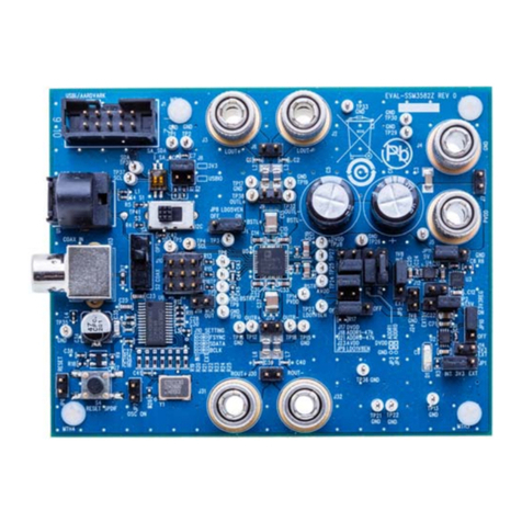
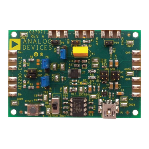
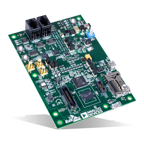
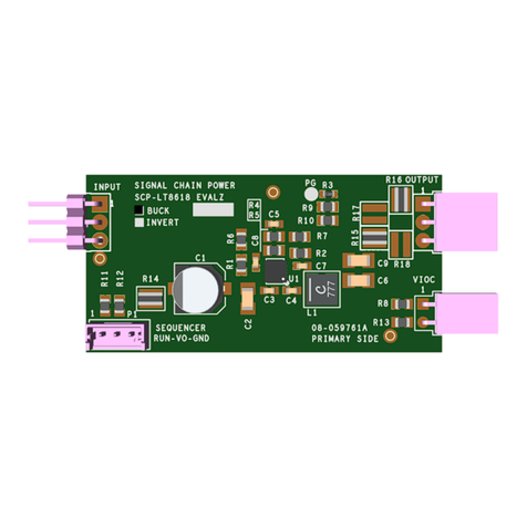
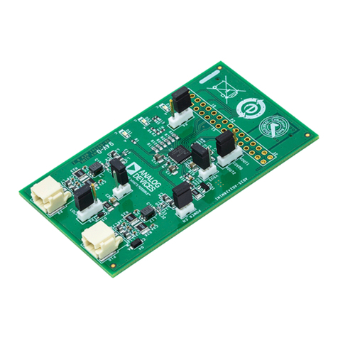
The ADP1071-1 E VA L Z is shown in Figure 1 and Figure 2. The
circuit components on the ADP1071-1 E VA L Z are described as
follows:
•The input filter consists of a capacitor bank including
Capacitor 24 (C24) to Capacitor 57 (C57).
•Q3 is an N channel, metal-oxide semiconductor field effect
transistor (MOSFET) used as the main switch on the
primary side.
•Transformer T1 provides isolation.
•The secondary side of the circuitry has three windings
followed by one rectifying diode and one resistor/capacitor
(RC) snubber.
•The output filter consists of two capacitors for each of the
rails. These capacitors include C60 and C65 at the 24 V
rail, C62 and C66 at the 5.5 V rail, and C7 and C67 at the
−15 V rail.
The snubber for the main switch is composed of D11 and D12.
The ADP1071-1 flyback controller (U1) is the power controller.
The power controller integrates gate drive for driving the
primary switch and synchronous rectifier based on the Analog
Devices, Inc., iCoupler® technolog y.
During startup, U1 is powered by the J2 or J4 input via an external
start-up circuit (Q7, R17, D5, or C38). When switching and
power conversion starts, the auxiliary winding provides power
to the VREG1 pin. R15 is the sense resistor that senses the
primary current.
TRANSFORMER
The transformer has 10 pins and five windings, including
primary winding (Pin 4 to Pin 3), auxiliary winding (Pin 2 to
Pin 1), and three output windings (Pin 6 to Pin 7, Pin 8 to Pin 9,
and Pin 9 to Pin 10).
4
PRI
18VDC TO 36VDC
66kHz
AUX
10V AND 20mAOUTPUT WINDING
15V AND 200mA
OUTPUT WINDING
5.5V AND 500mA
OUTPUT WINDING
24V AND 400mA
3
2
1
6
7
8
9
10
17050-003
Figure 3. Transformer Diagram
CONNECTORS
The connections to the ADP1071-1EVA LZ are shown in Table 1.
Table 1. Evaluation Board Connections
Connector Pin Function
J2 Pin 1, VIN+, dc input
Pin 2, VIN−, ground return for dc input
J5 Pin 1, 24 VDC output
Pin 2, 5.5 VDC output
Pin 3, GND, return for dc output
DC
CAUTION
The ADP1071-1 E VA L Z uses high voltages. Take extreme
caution, especially on the primary side, to ensure safety. It is
advised to switch off the evaluation board when not in use. Use
a current limited, isolated dc source at the input.
