Apro HERMIT Series Owner's manual

November 2010
Product Specification
Industrial micro IDE Flash Module (MIF)
- HERMIT Series -
Doc-No: 100-XMIFHA-02V0

This document is for information use only and is subject to change without prior notice. APRO Co., Ltd. assumes no
responsibility for any errors that may appear in this document, nor for incidental or consequential damages resulting from
the furnishing, performance or use of this material. No part of this document may be reproduced, transmitted, transcribed,
stored in a retrievable manner or translated into any language or computer language, in any form or by any means,
electronic, mechanical, magnetic, optical, chemical, manual or otherwise, without the prior written consent of an officer of
APRO Co., Ltd..
All parts of the APRO documentation are protected by copyright law and all rights are reserved.
APRO and the APRO logo are registered trademarks of APRO Co., Ltd..
Product names mentioned herein are for identification purposes only and may be trademarks and/or registered
trademarks of their respective companies.
© 2010 APRO Corporation. All rights reserved.
Revision History
Revision Description Date
1.0 Initial release 2008/12/23
2.0 New front label released 2010/11/11

CONTENTS
Industrial micro IDE Flash (MIF) Module - HERMIT Series © 2010 APRO Co., Ltd.
i
CONTENTS
1. INTRODUCTION........................................................................................................................................ 1
1.1. SCOPE...................................................................................................................................................... 2
1.2. SYSTEM FEATURES ................................................................................................................................. 2
1.3. ATA/ATAPI-6 STANDARD ....................................................................................................................... 2
1.4. TECHNOLOGY INDEPENDENCE -STATIC WEAR LEVELING.................................................................... 2
2. PRODUCT SPECIFICATIONS ..................................................................................................................... 3
2.1. SYSTEM ENVIRONMENTAL SPECIFICATIONS.......................................................................................... 3
2.2. SYSTEM POWER REQUIREMENTS ........................................................................................................... 3
2.3. SYSTEM PERFORMANCE ......................................................................................................................... 3
2.4. SYSTEM RELIABILITY.............................................................................................................................. 4
2.5. PHYSICAL SPECIFICATIONS .................................................................................................................... 4
2.6. CAPACITY SPECIFICATIONS..................................................................................................................... 7
3. INTERFACE DESCRIPTION ....................................................................................................................... 9
3.1. PHYSICAL DESCRIPTION ......................................................................................................................... 9
3.2. PIN ASSIGNMENTS .................................................................................................................................. 9
3.3. ELECTRICAL DESCRIPTION................................................................................................................... 10
3.4. ELECTRICAL SPECIFICATION.................................................................................................................11
3.4.1. ABSOLUTE MAXIMUM RATING........................................................................................................... 12
3.4.2. RECOMMENDED OPERATING CONDITION ......................................................................................... 12
3.4.3. DC CHARACTERISTICS....................................................................................................................... 12
3.4.4. TIMING SPECIFICATIONS ................................................................................................................... 13
PIO MODE....................................................................................................................................................... 13

CONTENTS
Industrial micro IDE Flash (MIF) Module - HERMIT Series © 2010 APRO Co., Ltd.
ii
MULTIWORD DMA.......................................................................................................................................... 14
ULTRA DMAMODE.......................................................................................................................................... 15
4. COMMAND DESCRIPTIONS .................................................................................................................... 18
4.1. COMMAND SET...................................................................................................................................... 18
5. INSTALLATION PROCEDURE .................................................................................................................. 19
5.1. BEFORE UNPACKING ............................................................................................................................. 19
5.2. ESD PRECAUTIONS............................................................................................................................... 19
5.3. CONFIGURATION OF MIF..................................................................................................................... 19
5.4. MIFINSERTION AND REMOVING.......................................................................................................... 19
5.4.1. MIFINSERTION ................................................................................................................................. 19
5.4.2. MIFREMOVING................................................................................................................................. 21
5.5. IDE DEVICE SETUP /AUTO-DETECTION.............................................................................................. 21
5.6. PARTITION &FORMAT .......................................................................................................................... 21
ORDERING INFORMATION............................................................................................................................... 23
APPENDIX A. LIMITED WARRANTY.............................................................................................................. 24

1. Introduction
APRO Industrial 40/44-pin micro IDE Flash (MIF) Disk Hermit Series products are designed to follow ATA/ATAPI-6
standard. The main used Flash memories are Samsung SLC NAND Type Flash memory chips. The available Card
capacities are 128MB, 256MB, 512MB, 1GB, 2GB, 4GB and 8GB. The operating temperature grade is optional for
standard grade 0°C ~ 70°C and industrial grade -40°C ~ +85°C. The APRO Industrial 40/44-pin micro IDE Flash (MIF)
Disk Hermit Series are designed electrically compliant with the conventional IDE hard disk and support True IDE Mode.
The data transfer modes supports PIO mode 0~6, Multi Word DMA 0~4, or UDMA 0~5; Default setting are PIO mode-4 or
UDMA-4. Hermit Series MIF features an extremely light weight, reliable, low-profile form factor.
The APRO Industrial 40/44-pin MIF Hermit Series provides a high level interface to the host computer. This interface
allows a host computer to issue commands to the Flash Disk to read or write blocks of memory. The host addresses the
card in 512 byte sectors. Each sector is protected by a powerful 4 bits Error Correcting Code (ECC). APRO Industrial
40/44-pin micro IDE Flash (MIF) Disk Hermit Series, it uses intelligent controller which manages interface protocols, data
storage and retrieval as well as ECC, defect handling and diagnostics, power management and clock control.
Figure 1 shows a block diagram of the used high tech Industrial 40/44-pin micro IDE Flash (MIF) Disk Hermit Series
controller.
Flash Flash
Flash
Sequencer
and Control
Logic
EDC/ECC
Circuit
ROM
Code
RAM
Micro
processor
Buffer
Management
and Control
Control & Address
Signal
Data Signal
ATA Interface
ATA Host
Figure 1: micro IDE Flash Disk Controller Block Diagram
1 Industrial micro IDE Flash (MIF) Module - HERMIT Series © 2010 APRO Co., Ltd.

Industrial micro IDE Flash (MIF) Module - HERMIT Series © 2010 APRO Co., Ltd.
2
1.1. Scope
This document describes the features and specifications and installation guide of APRO’s Industrial 40/44-pin MIF Hermit
Series. In the appendix, there provides order information, warranty policy, RMA/DOA procedure for the most convenient
reference.
1.2. System Features
Non-volatile memory and no moving parts
SLC NAND type flash technology
Disk capacity from 128MB to 8GB
ATA interface and True IDE mode
Master/Slave Switch
Data transfer supports PIO-4 and UDMA-4 (Default setting)
Performance up to 40.0MB/sec
Automatic 4 bits error correction and retry capabilities
Supports power down commands and Auto stand-by / sleep modes.
+5 V ±10%or +3.3 V ±5%operation
40-pin MIF support pin-20 5V power-input.
MTBF > 3,000,000 hours.
Shock : 50g (Duration:10ms, 3 axes), compliance to IEC 68-2-27
Vibration : 5g (7 Hz to 2000 Hz, 3 axes), compliance to IEC 68-2-6
Rugged environment is working well
Very high performance, very low power consumption
Low weight, Noiseless
1.3. ATA/ATAPI-6 Standard
APRO Industrial 40/44-pin MIF disks are fully compatible with the ATA/ATAPI-6 standard.
1.4. Technology Independence - Static Wear Leveling
In order to gain the best management for flash memory, APRO Industrial CF Cards – Hermit series supports Static
Wear Leveling technology to manage the Flash system. The life of flash memory is limited; the management is to
increase the life of the flash product.
A static wear-leveling algorithm evenly distributes data over an entire Flash cell array and searches for the
least used physical blocks. The identified low cycled sectors are used to write the data to those locations. If
blocks are empty, the write occurs normally. If blocks contain static data, it moves that data to a more heavily
used location before it moves the newly written data. The static wear leveling maximizes effective endurance
Flash array compared to no wear leveling or dynamic wear leveling.

Industrial micro IDE Flash (MIF) Module - HERMIT Series © 2010 APRO Co., Ltd.
3
2. Product Specifications
For all the following specifications, values are defined at ambient temperature and nominal supply voltage unless
otherwise stated.
2.1. System Environmental Specifications
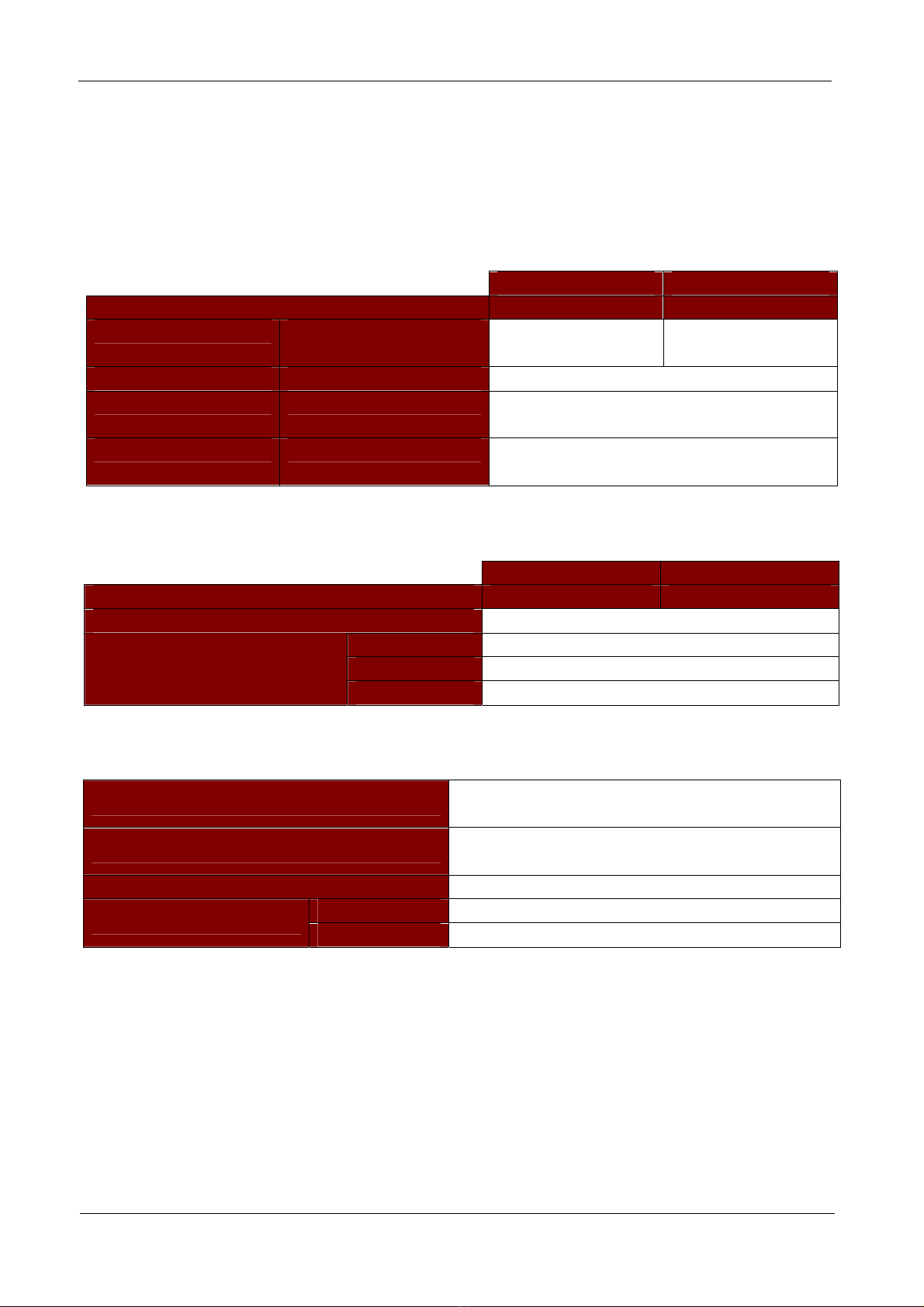
Table 1: Environmental Specification
Standard Grade Industrial Grade
APRO Industrial Hermit Series MIF SxMIFxxxx-HACSC Series WxMIFxxx-HAISI- Series
Temperature Operating:
Non-operating:
0ºC ~ +70ºC
-55ºC ~ +95ºC
-40ºC ~ +85ºC
-55ºC ~ +95ºC
Humidity Operating & Non-operating: 10% ~ 95% non-condensing
Vibration Operating & Non-operating: 5g (7 Hz to 2000 Hz, 3 axes),
compliance to IEC 68-2-6
Shock Operating & Non-operating: 50g (Duration:10ms, 3 axes),
compliance to IEC 68-2-27
2.2. System Power Requirements
Table 2: Power Requirement
Standard Grade Industrial Grade
APRO Industrial Hermit Series MIF SxMIFxxxx-HACSC Series WxMIFxxx-HAISI- Series
DC Input Voltage (VCC) 100mV max. ripple(p-p) +5 V ±10%
Reading Mode : Single Channel: 69mA (max.) / Duel Channel: 128mA (max.)
Writing Mode : Single Channel: 48mA (max.) / Duel Channel: 118mA (max.)
+5V Current
(Maximum average value) Sleeping Mode : Single Channel: 1.2mA (max.) / Duel Channel: 1.8mA (max.)
2.3. System Performance
Table 3: System Performances
Data Transfer Mode supporting - PIO mode : 0,1,2,3,4,5,6 (Default PIO-4)
- UDMA Mode: 0,1,2,3,4,5 (Default UDMA-4)
Data Transfer Rate To/Form Host 16.6Mybtes/sec burst under PIO Mode 4
66.6Mbytes/sec burst under UDMA-4 Mode
Average Access Time 0.2 ms(estimated)
Sequential Read 40 Mbytes/sec Max.
Maximum Performance Sequential Write 17 Mbytes/sec Max.
Note:
(1). All values quoted are typically at 25oC and nominal supply voltage.
(2). Testing of the Industrial 40/44-pin micro IDE Flash (MIF) Disk Hermit Series maximum performance was performed under the
following platform:
- Computer with AMD 3.0GHz processor
- Windows XP Professional operating system
- IDE transfer mode: Ultra DMA mode 4
- IDE Flash Disk capacity: 4GB

Industrial micro IDE Flash (MIF) Module - HERMIT Series © 2010 APRO Co., Ltd.
4
2.4. System Reliability
Table 4: System Reliability
MTBF >3,000,000 hours
Data Reliability <1 non-recoverable error in 1014bits read
<1 erroneous correction in 1020bits read
Wear-leveling Algorithms Supportive
ECC Technology 4 bits Error Connection Code
Endurance Greater than 2,000,000 cycles Logically contributed by
Wear-leveling and advanced bad sector management
Data Retention 10 years
2.5. Physical Specifications
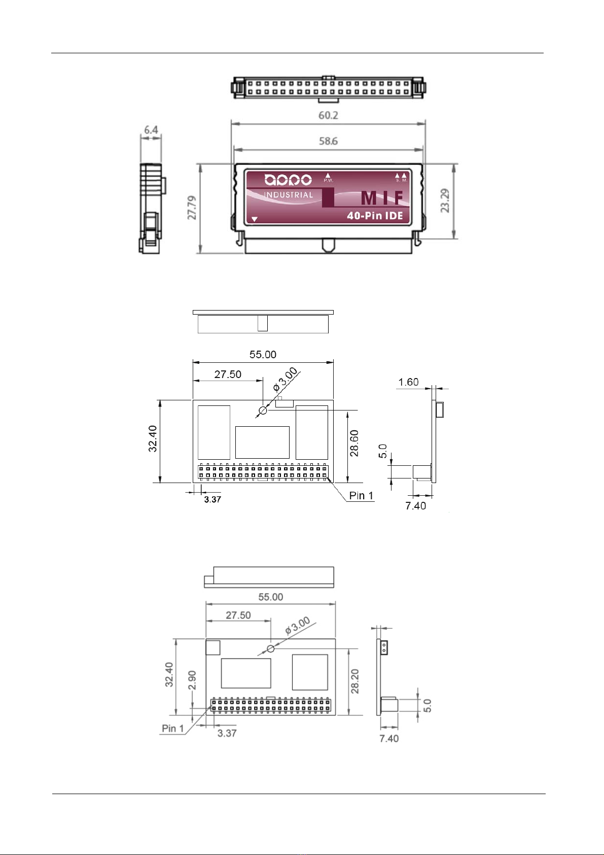
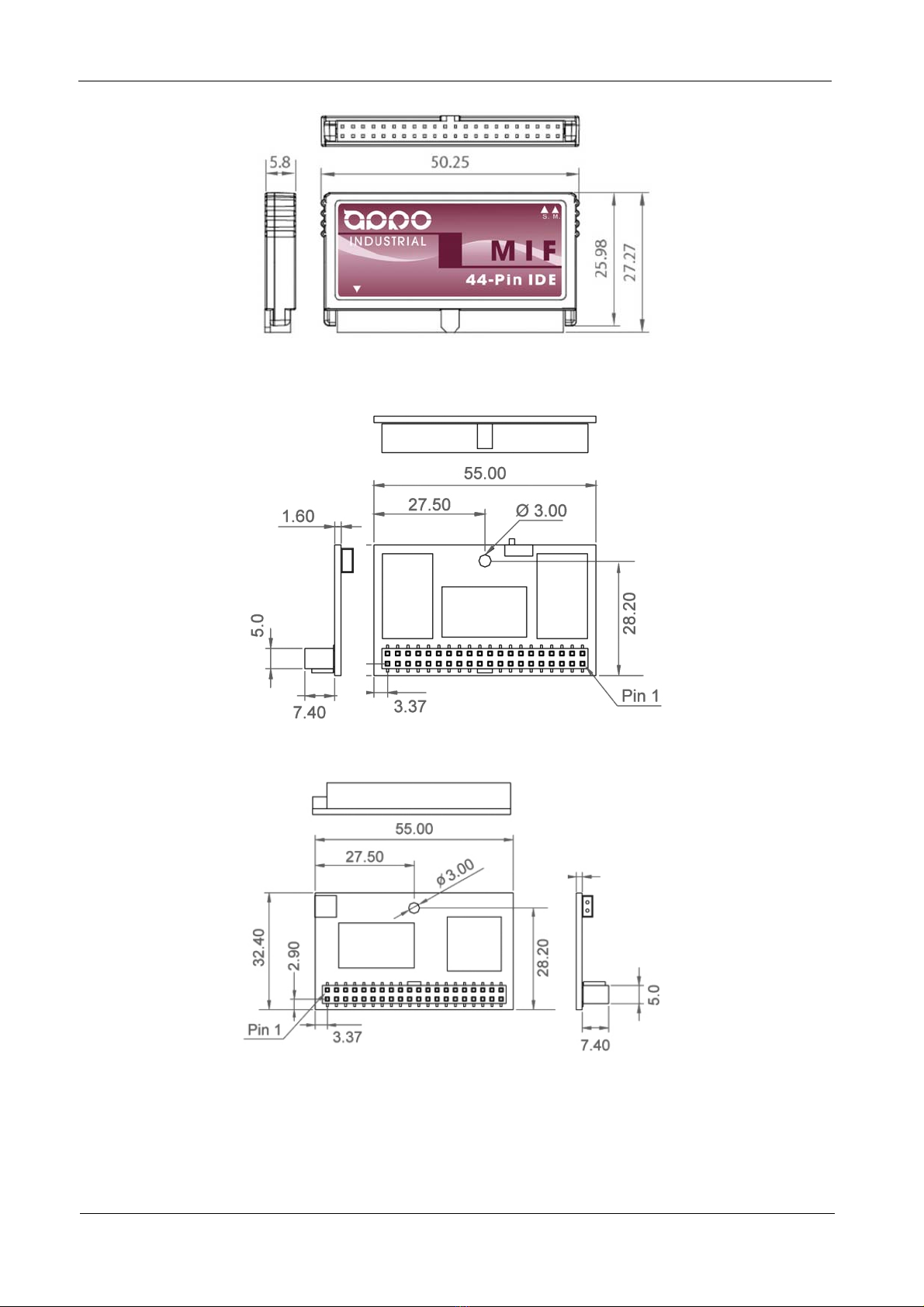
Refer to Table 5 and see Figure 3 for Industrial 40/44-pin MIF physical specifications and dimensions.
Table 5: Physical Specifications
40-pin MIF
Orientation : Vertical Type Horizontal Type
Length: 60.20 mm 55.00 mm
Width: 27.79 mm 32.40 mm
Thickness: 6.40 mm 7.40 mm
G. W. : 20 g 15 g
44-pin MIF
Orientation : Vertical Type Horizontal Type
Length: 50.25 mm 48.00 mm
Width: 27.27 mm 32.60 mm
Thickness: 5.80 mm 4.50 mm
G. W. : 15 g 10 g

Industrial micro IDE Flash (MIF) Module - HERMIT Series © 2010 APRO Co., Ltd.
5
Figure 2 - 40-pin Vertical Type MIF
Figure 3 – 40-pin Horizontal-leftward Type MIF
Figure 4 - 40-pin Horizontal-rightward Type MIF

Industrial micro IDE Flash (MIF) Module - HERMIT Series © 2010 APRO Co., Ltd.
6
Figure 5 - 44-pin Vertical Type MIF
Figure 6 - 44-pin Horizontal-leftward Type MIF
Figure 7 - 44-pin Horizontal-rightward Type MIF

Industrial micro IDE Flash (MIF) Module - HERMIT Series © 2010 APRO Co., Ltd.
7
2.6. Capacity Specifications
APRO Industrial 40/44-pin micro IDE Flash (MIF) Disks are built-in mainly Samsung NAND Type SLC Flash memory chips.
The Table 6 shows the equipollent part number of applied Samsung Flash memory chips for each card.
Table 6: Card Configuration vs. Samsung NAND SLC part number
Card Capacity Samsung SLC Flash Memory Part Number * Q’TY
128MB Standard Grade:
Industrial Grade:
K9F1G08U0A-PCB0(1Gb) or equipollent * 1
K9F1G08U0A-PIB0 (1Gb) or equipollent * 1
256MB
Standard Grade:
Industrial Grade:
K9F2G08U0A-PCB0 (2Gb) or equipollent * 1
K9F1G08U0A-PCB0(1Gb) or equipollent * 2
K9F2G08U0A-PIB0 (2Gb) or equipollent * 1
K9F1G08U0A-PIB0 (1Gb) or equipollent * 2
512MB
Standard Grade:
Industrial Grade:
K9F4G08U0M-PCB0 (4Gb) or equipollent * 1
K9F2G08U0A-PCB0 (2Gb) or equipollent * 2
K9F1G08U0A-PCB0(1Gb) or equipollent * 4
K9F4G08U0M-PIB0 (4Gb) or equipollent * 1
K9F2G08U0A-PIB0 (2Gb) or equipollent * 2
K9F1G08U0A-PIB0 (1Gb) or equipollent * 4
1GB
Standard Grade:
Industrial Grade:
K9K8G08U0M-PCB0 (8Gb) or equipollent * 1
K9F4G08U0M-PCB0 (4Gb) or equipollent * 2
K9K8G08U0M-PIB0 (8Gb) or equipollent * 1
K9F4G08U0M-PIB0 (4Gb) or equipollent * 2
2GB
Standard Grade:
Industrial Grade:
K9WAG08U1M-PCB0 (16Gb) or equipollent *1
K9K8G08U0M-PCB0 (8Gb) or equipollent *2
K9WAG08U1M-PIB0 (16Gb) or equipollent *1
K9K8G08U0M-PIB0 (8Gb) or equipollent *2
4GB
Standard Grade:
Industrial Grade:
K9WAG08U1M-PCB0 (16Gb) or equipollent *2
K9K8G08U0M-PCB0 (8Gb) or equipollent *4
K9WAG08U1M-PIB0 (16Gb) or equipollent *2
K9K8G08U0M-PIB0 (8Gb) or equipollent *4
8GB Standard Grade:
Industrial Grade:
K9WAG08U1M-PCB0 (16Gb) or equipollent *4
K9WAG08U1M-PIB0 (16Gb) or equipollent *4

Industrial micro IDE Flash (MIF) Module - HERMIT Series © 2010 APRO Co., Ltd.
8
The table 7 shows the specific capacity for the various models and the default number of heads, sectors/track and
cylinders.
Table 7: Model Capacity
Unformatted Capacity Default Cylinder Default Head Default Sector Default CHS
Capacity
128MB 500 16 32 256,000
256MB 1,000 16 32 512,000
512MB 1,015 16 63 1,023,120
1,024MB 2,031 16 63 2,047,248
2.04GB 4,063 16 63 4,095,504
4GB 8,146 16 63 8,211,168
8GB 16,000 16 63 16,128,000

Industrial micro IDE Flash (MIF) Module - HERMIT Series © 2010 APRO Co., Ltd.
9
3. Interface Description
3.1. Physical Description
The pin 1 ~ pin 44 are for IDE interface.
Figure 8- Vertical Type 40-pin IDE Connector Figure 8 - Horizontal Type 40-pin IDE Connector
Figure 9 - Vertical Type 44-pin IDE Connector Figure 10 - Horizontal Type 44-pin IDE Connector
3.2. Pin Assignments
Signals whose source is the host is designated as inputs while signals that the Industrial 44-pin micro IDE Flash (MIF)
Disk sources are outputs. The pin assignments are listed in below table 8.
Table 8: Pin Assignments
Pin No. Signal Name Description Pin No. Pin Name Description
1 HRESET Host Reset 2 GND Ground
3 HDB[7] Host Data Bit 7 4 HDB[8] Host Data Bit 8
5 HDB[6] Host Data Bit 6 6 HDB[9] Host Data Bit 9
7 HDB[5] Host Data Bit 5 8 HDB[10] Host Data Bit 10
9 HDB[4] Host Data Bit 4 10 HDB[11] Host Data Bit 11
11 HDB[3] Host Data Bit 3 12 HDB[12] Host Data Bit 12
13 HDB[2] Host Data Bit 2 14 HDB[13] Host Data Bit 13
15 HDB[1] Host Data Bit 1 16 HDB[14] Host Data Bit 14
17 HDB[0] Host Data Bit 0 18 HDB[15] Host Data Bit 15

Industrial micro IDE Flash (MIF) Module - HERMIT Series © 2010 APRO Co., Ltd.
10
40-pin MIF VCC1Supply Voltage
19 GND Ground 20
44-pin MIF KEY1Key-pin
21 DMARQ DMA Request 22 GND Ground
HIOW3Host I/O Write
23 STOP4Stop Ultra DMA burst 24 24 GND
HIOR3Host I/O Read
HDMARDY4Ultra DMA ready25
HSTROBE4Ultra DMA data strobe
26 GND Ground
IORDY3I/O Ready
DDMARDY4Ultra DMA ready27
DSTROBE4Ultra DMA data strobe
28 CSEL Cable select
29 DMACK DMA Acknowledge 30 GND Ground
31 INTRQ Interrupt Request 32 IOCS16 CS I/O 16-Bit
33 HAB[1] Host Address Bit 1 34 PDIAG Passed Diagnostic
35 HAB[0] Host Address Bit 0 36 HAB[2] Host Address Bit 2
37 CS0 Chip Select 0 38 CS1 Chip Select 1
39 DASP Drive Active 40 GND Ground
41 VCC Supply Voltage 42 VCC Supply Voltage
43 GND Ground 442NC Not Connected
1. According to ATA standard, the pin-20 in 40-pin module is defined as VCC to reduce the need for external power connector. Pin-20 in
44-pin module is defined as KEY.
2. The 40-pin module does not include pins 41-44.
NC = These pins are not connected within.
3. Signal usage in PIO & Multiword DMA mode.
4. Signal usage in Ultra DMA mode.
3.3. Electrical Description
The Industrial 40/44-pin micro IDE Flash (MIF) Disk Hermit Series is optimized for operation with hosts. .Table 9:
describes the signals of 40/44-pin interface.
Table 9: Signal Description
Pin No. Signal Name Type Description
1 HRESET- I Host reset signal, High: Reset.
37 CS0- I Chip select CS0
38 CS1- I Chip select CS1
31 INTRQ O Host interrupt signal.
HIOR-3I/O read strobe signal.
HDMARDY-4DMA ready during Ultra DMA data in burst
25
HSTROBE4
I
Data strobe during Ultra DMA data out burst
HIOW-3I/O write strobe signal.
23 STOP4I Stop during Ultra DMA data bursts
32 IOCS16- O Asserted in 16-bit access.
IORDY3I/O Ready Signal
DDMARDY-4DMA ready during Ultra DMA data out burst27
DSTROBE4
O
Data strobe during Ultra DMA data in burst

Industrial micro IDE Flash (MIF) Module - HERMIT Series © 2010 APRO Co., Ltd.
11
18, 16, 14, 12,
10, 8, 6, 4, 3,
5, 7, 9, 11, 13,
15, 17
HDB[15:0] I/O Host data bus
33, 35, 36 HAB[2:0] I/O Host Address bus
28 CSEL- I I
Master/Slave select signal (cable select signal).
Low: Device operates as a master, High: Device operates as a slave.
Switch used.
39 DASP- I/O
Used as an input port to check in the master mode to see if the slave
is present or not, and as an output port to check in the slave mode to
see if the slave for the master is present or not.
34 PDIAG- I/O
Used as an input port to evaluate the result of slave diagnosis in the
master mode, and as an output port to return the result of diagnosis
to the master.
21 DMARQ O DMA Request.
29 DMACK- I DMA Acknowledge.
201, 412, 422VCC VCC Connect to VCC
2, 19, 22, 24,
26, 30, 40, 432
GND GND Connect to GND.
442NC N/A Not used. Please do not connect.
1. According to ATA standard, the pin-20 in 40-pin module is defined as VCC to reduce the need for external power connector. Pin-20 in
44-pin module is defined as KEY.
2. The 40-pin module does not include pins 41-44.
NC = These pins are not connected within.
3. Signal usage in PIO & Multiword DMA mode.
4. Signal usage in Ultra DMA mode.
3.4. Electrical Specification
Table 11, Table 12, and Table 13 defines all D.C. Characteristics for the Industrial 40/44-pin micro IDE Flash (MIF) Disk
Hermit Series. Unless otherwise stated, a condition is as below Table 10:
Table 10: Electrical Condition
SxMIFxxxx-HACSC Series WxMIFxxxx-HAISI- Series
Vcch = 5V ±10% or 3.3V ± 10%
Vccf = 3.3V ± 10%
Ta = 0°C to 70°C
Vcch = 5V ±10% or 3.3V ± 10%
Vccf = 3.3V ± 10%
Ta = -40°C to 85°C

Industrial micro IDE Flash (MIF) Module - HERMIT Series © 2010 APRO Co., Ltd.
12
3.4.1. Absolute Maximum Rating
Table 11: Absolute Maximum Rating
Parameter Symbol Rating Unit
DC Power Supply VDD - VSS -0.3 ~ +5.5 V
Input voltage VIN V
SS-0.3 ~ VDD+0.3 V
Output voltage VOUT V
SS-0.3 ~ VDD+0.3 V
Standard: -10 ~ +70 °C
Operating Temperature TA
Industrial: -40 ~ +85 °C
Standard: -20 ~ +80 °C
Storage Temperature TST
Industrial: -55 ~ +95 °C
3.4.2. Recommended Operating Condition
Table 12: Recommended Operating Condition
3.4.3. DC Characteristics
Table 13: DC Characteristics
Value
Parameter Symbol Min Standard Max Unit
Power Supply VCCH 4.5 5.0 5.5 V
Power Supply VCCF 3.0 3.3 3.6 V
Input low voltage VIL -0.3 0.8 V
Input high voltage VIH 2.0 Vcc+0.3 V
Output low voltage VOL
0.45 (at
4mA) V
Output high voltage VOH 2.4 (at
1mA) V
Operating CurrentV
Sleep Mode
Operation
Icc
1.4
140
mA
mA
Input Leakage Current ILI ±10 uA
Output leakage current LLO ±10 μA
Input/output Capacitance CI/O 10 pF

Industrial micro IDE Flash (MIF) Module - HERMIT Series © 2010 APRO Co., Ltd.
13
3.4.4. Timing Specifications
PIO Mode
Figure 11: Read/Write Timing Diagram, PIO Mode
Table 14: Read/Write Timing Specifications, PIO Mode 0-4
PIO timing parameters Mode 0 Mode 1 Mode 2 Mode 3 Mode 4
t0Cycle time (min.) 600 383 240 180 120
t1Address valid to HIOR-/HIOW- setup (min.) 70 50 30 30 25
t2HIOR-/HIOW- 16-bit (min.) 165 125 100 80 70
t2HIOR-/HIOW- Register 8-bit (min.) 290 290 290 80 70
t2i HIOR-/HIOW- recovery time (min.) - - - 70 25
t3HIOW- data setup (min.) 60 45 30 30 20
t4HIOW- data hold (min.) 30 20 15 10 10
t5HIOR- data setup (min.) 50 35 20 20 20
t6HIOR- data hold (min.) 5 5 5 5 5
t6z HIOR- data tri-state (max.) 30 30 30 30 30
t7Address valid to IOCS16- assertion (max.) 90 50 40 n/a n/a
t8Address valid to IOCS16- released (max.) 60 45 30 n/a n/a
t9HIOR-/HIOW- to address valid hold 20 15 10 10 10
tRD Read data valid to IORDY active (min.) 0 0 0 0 0
tAIORDY setup time 35 35 35 35 35
tBIORDY pulse width (max.) 1250 1250 1250 1250 1250
tCIORDY assertion to release (max.) 5 5 5 5 5

Industrial micro IDE Flash (MIF) Module - HERMIT Series © 2010 APRO Co., Ltd.
14
Multiword DMA
Figure 12: Read/Write Timing Diagram, Multiword DMA Mode
Table 15: Read/Write Timing Specifications, Multiword DMA Mode 0-2
Multiword DMA timing parameters Mode 0 Mode 1 Mode 2
t0Cycle time (min.) 480 150 120
tDHIOR-/HIOW- assertion width (min.) 215 80 70
tEHIOR- data access (max.) 150 60 50
tFHIOR- data hold (min.) 5 5 5
tGHIOR-/HIOW- data setup (min.) 100 30 20
tHHIOW- data hold (min.) 20 15 10
tIDMACK to HIOR-/HIOW- setup (min.) 0 0 0
tJHIOR-/HIOW- to DMACK hold (min.) 20 5 5
tKR HIOR- negated width (min.) 50 50 25
tKW HIOW- negated width (min.) 215 50 25
tLR HIOR- to DMARQ delay (max.) 120 40 35
tLW HIOW- to DMARQ delay (max.) 40 40 35
tMCS1-, CS0- valid to HIOR-/HIOW- 50 30 25
tNCS1-, CS0- hold 15 10 10
tZDMACK- 20 25 25

Industrial micro IDE Flash (MIF) Module - HERMIT Series © 2010 APRO Co., Ltd.
15
Ultra DMA mode
Figure 13: Ultra DMA Mode Data-in Burst Initiation Timing Diagram
Figure 14: Ultra DMA Mode Data-out Burst Initiation Timing Diagram

Industrial micro IDE Flash (MIF) Module - HERMIT Series © 2010 APRO Co., Ltd.
16
Figure 15: Sustained Ultra DMA Mode Data-in Burst Timing Diagram
Figure 25: Sustained Ultra DMA Mode Data-out Burst Timing Diagram
Table of contents