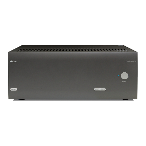
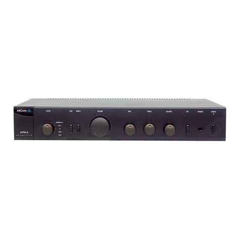
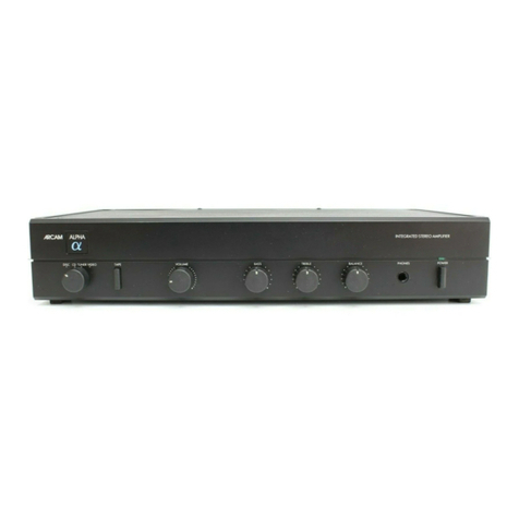
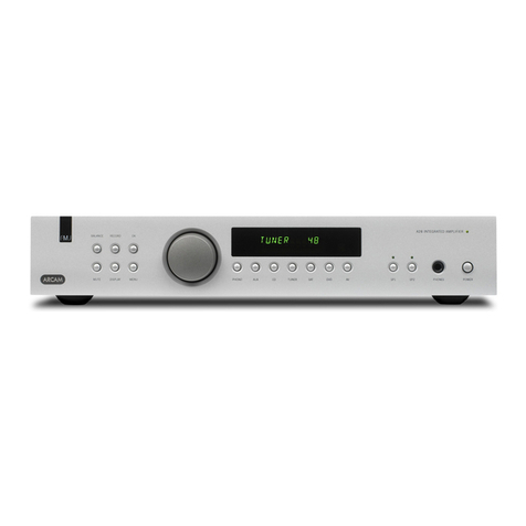
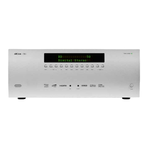
Arcam C30, P35 User manual

Service
Manual
C30 Pre-AmpliÞer
Issue 1.0
ARCAM
Bringing music & movies to life

Contents List
!
Circuit description
!
Circuit diagrams
o L958AY power supply board
o L965AY pre-amp board
o L928AY display board
o L870AY phono board
o L955AY multi-channel board
!
Transformers
o L923TX – 115/230VAC toroidal
o L922TX – 100VAC toroidal
o L907TX – 100VAC frame
!
Exploded view diagram
!
Mechanical & packing parts list
!
Circuit board silk screen & parts list
o L928AY display board
o L955AY multi-channel board
o L958AY power supply board
o L965AY pre-amp board
o L870AY phono board

C30 preamplifier circuit description.
Introduction
The C30 pre-amplifier uses pre-amp input
switching/control and display boards that are
very similar in design to the boards used in
both the Diva A85/A90 and Fmj A32
integrated amplifiers and as such you may
already be familiar with the layout and
topologies of these boards. The C30 boasts a
very much over-engineered power supply and
output stage that is designed to bring the very
best out of the existing Pre-amp input
switching board.
The main PCB L958AY also contains output
buffers for the unbalanced outputs to drive
long cables and balanced line drivers. A
headphone amplifier is included to drive low
impedance headphones down to 32 Ohm.
For description of the pre-amplifier switching
and control board see the section...
Power supply.
The mains input comes in via SKT1. Two Y
caps return common mode noise to the
chassis ground and an X cap reduces any
single ended noise. The 1M5 resistor
following this is in place to discharge the
capacitors when the unit is turned off.
The mains selector switch, which follows the
resistor, changes the configuration of the
transformer windings from series for 230V to
parallel for 115V. Tx1 is a standby
transformer it powers the microcontroller at all
times so that the unit can be put into and out
of standby. To reduce voltage losses after
this transformer, low forward drop diodes are
used. A low drop out regulator follows to
create the 4.5v(D) supply; this supply powers
the micro and digital circuits.
The primary of the Toroid supply transformer
Tx2 is connected to CON3 and the power to
this is switched on and off by the relay RLY1.
The transformer has a number of secondary
outputs and we use separate taps and bridge
rectifiers networks followed by bulk
capacitors to smooth the ripple. The voltages
generated are +24V and -24V for the main
analogue supplies, +46V for the HT supply to
the VFD, and +18V, which is used to power
the trigger output. The smoothed +/- 24V
then goes through regulators REG 2 and
REG 5 to create +/- 18V this is passed the
pre-amplifier PCB via CON4. Another set of
regulators REG 3 and REG 6 follow taking
the 18V and creating a +/-15V supply that is
available for add on modules such as the 7.1
channel input board. A 5v supply is derived
via regulator REG 4 from the 18V to run the
headphone amplifier.
Mains detect.
A mains present detector runs from the
standby transformer, this detects the loss of
mains using a peak hold circuit based around
D7/TR1/DZ1 and TR2. If the power is lost this
piece of circuitry sends a flag to the
microcontroller so it can mute the outputs
and shut down the unit. See Fig 1 for notes
on protection modes.
12v trigger and RC5 receiver.
The trigger output on SKT2 is driven through
TR4 to provide a current limited supply at
around 13V.
IC1 A and Bare used to demodulate
incoming RC5 from socket SKT2. IC1A is a
band-pass filter centred on 36KHz. This is
followed by a peak detector circuit that
demodulates the incoming signal.
Fig 1. Protection and mute mode and
measurements.
Prot line Measured at. Working
reading
AC present Resistor R12 +4.5v
Mute* Con 8 Pin 5 +4.5v
Standby* Resistor R5 at
point P18
.7v
Trigger ResistorR10 at
point P54
+1.8v

Pre-amp input card.
Introduction.
The pre-amp stage is a high-performance,
DC coupled design with microprocessor
control of input select, two independent tape
loops, electronic volume control and tone
bypass.
It features a discrete power supply and low-
noise linear circuitry to obtain exceptionally
low distortion and noise performance results.
Power supply stage
The secondary transformer output windings
from the main toroid transformer are
connected to SK300. The A.C voltage is
rectified and smoothed by D300, D301, D306,
D307 and C300, C301. The unregulated
voltage should be around +/- 27 V obviously
this is dependent on the A.C level at the
mains inlet socket; F300 and F301 are the
secondary A.C s.m fuses these are rated at
2A.
The voltage regulators are discrete emitter
followers the +15 voltage stage is described
below as the –15 v stage is effectively very
similar.
Q300 and R300 act as a constant current
source, supplying around 7mA into D310.
C302 and C314 reduce ripple and broadband
noise on the zener diode. Q305 and Q306
form a complementary Darlington NPN
transistor, which is configured as an emitter
follower producing +15v at it’s output. C303 is
to provide bulk charge storage and to reduce
the AC output impedance of the power
supply.
D302 prevents reverse bias of the supply
during power down.
Z301 is a conventional LM317 type circuit to
regulate the +15v rail down to +5v for the
tone and volume control circuits.
Input switching
Each of the inputs has a pair of diodes to the
+/- 15v rails to prevent static spikes from
causing damage to the CMOS multiplexors.
In addition, there is a simple resistor-
capacitor filter with a corner frequency of
approximately 340kHz to remove any
unwanted high frequency interference from
the signal. This uses high quality WIMA
polypropylene capacitors for the best
possible performance.
Z104 (left) and Z105 (right) are the main
input multiplexers, which are configured in a
“virtual earth” unity gain arrangement with
Z115 and Z116. This is an inverting circuit
topology and the phase is corrected by the
inverting volume control.
Z115B (left) and Z116B (right) are the
integrating servos, which remove any D.C
coefficient from the Analogue input switching
stages before the signal is passed onto the
following stages, R180 and C147 (left) form a
filter to remove any broadband noise from the
servo output and to improve the speed
response.
Z100 –Z103 are the Tape output selectors
these are non-inverting and the outputs are
again buffered by Z9 a/b and Z10 a/b before
arriving at the two tape loop outputs.
Z106 is configured as a double pole
changeover switch and is used to select the
tone controls or direct by pass mode. (See
below for more information).
Tone controls
The tone control stage is non-inverting and
uses a gyrating bell filter for the Bass and a
simple shelving filter for the high frequencies,
the left channel only will be described.
The input is attenuated by –6dB and biased
to a voltage of +2.5v D.C by C111,R113,
R112,R110,R111 and C110. This is so the
signals fall within the 0 – 5v D.C required by
the digital potentiometer Z108.
Z111B and its associated components form
an active equivalent of a series resonant LCR
circuit. This has an impedance minimum 5.4k
at around 80.
The digital pots Z108D and Z108A control the
bass and treble respectively, this
accomplished by moving the wiper connected
to the frequency-sensitive impedance
between to non inverting and inverting
terminals of Z112A, effectively changing the
ratio of feedback boost and feed forward
attenuation of the circuit at the desired
frequencies, thus providing a EQ gain control
that is on a logarithmic scale, with the use of
a linear pot.
Z112B provides the 6dB of gain necessary to
bring the nominal level of signal back to unity
C116 and C117 remove the 2.5VDC offset
from the output to prevent click and bangs
when the tone control are activated.
Z108 is controlled by a simple 3-wire serial
interface from the microprocessor. Each of
the digital lines has it’s own ground return
these are terminated at the GND pin of the
chip to minimize any electromagnetic
interference.
Volume control
Z107 is a VSDVC electronic volume control
IC. It works in conjunction with external op-
amp Z117a/b by varying the feed-forward and
feedback resistors in an inverting gain
configuration, the volume control is driven by
3-wire data from the H8 micro on the display
board – if the control receives no data it will
remain in Audio mute mode.
Relay RLY100 shunts the output of the Op-
amps to ground at switch on – power down
and when switching between inputs.
Audio output stages.
The Audio output stage contains the
buffered, un-buffered and balanced outputs
as well as the headphone driver.
The audio signal from the preamp PCB
enters the board on CON100 and the direct
signal goes straight to the output via the mute
relays RlY100A and RLY101B. A buffered
version of the signal is created by IC100 and
IC101. IC100 and IC101 are op-amps
configured as unity gain non-inverting
buffers.
The C30 also has a Balance XLR output
stage that drives into the balanced line
drivers IC103 and IC104. These line divers
create a transformer-less balanced output.
Headphone Output.
The selected audio output signal is driven
into the headphone driver IC102; this signal
then passes through CON101 and CON102
to the headphone socket SKT101. The mute
signal passes through the switch contacts in
the headphone socket so when headphones
are inserted the main outputs are relay
muted.
Please note: this means that if the
headphone sockets control contacts are
faulty or damaged the unit will be
permanently stuck in audio mute mode.
RC5 remote code assignment change.
The C30 has the ability to switch between
RC5 system code 16* and 19, we can
achieve this by pressing and holding the
Phono/Aux – CD and AV – DVD buttons
simultaneously the display will show.
RC5 System Code
16*
We can toggle the system code using the
rotary encoder.

Display board
The display board is very similar in design to
the board that has been used for many years
in the A85 family of products inc FMJ A32
and as such those of you familiar with these
products will know there way around this
board, a full description follows.
The power supply rails for the display board
are derived from the main board we should
expect to see the below supplies in place (Fig
2.)
Fig 2 Display board power supply pins
Power supply Pin number of SK1
+ 5v D.C (micro) Pin 14
+ 5v D.C Pin 1
+ 46v D.C for VFD HT Pin 3
Please note: the H8 micro is very critical of
the +5v supply and as such the unit may
crash or fail to power up during use if the +5v
supply drops below 4.5v.
H8 Microprocessor
The H8 micro at location Z1 is pre-
programmed by Arcam using a flash-
programming module and cannot be
reprogrammed in the field unless you have
access to the appropriate hardware and
software.
The H8 forms the heart of the C30 and takes
on all major control functions including.
1. Control of the input switching.
2. Controls the action of the volume cont.
3. Monitors protection status and mute lines
A85/A90/A32 only.
4. Sends display information to the VFD.
5. Receives and decodes RC5 data.
6. Receives data from rear panel remote
input.
7. Stores setting information via 24C02 E-
prom.
At initial power up the H8 micro is reset by Z2
aDS1233 econo reset package.
The input switching information is driven out
to the Pre-amp card via the 9 select lines that
appear on Pins 14 – 22 of SK3.
The Volume control and tone control circuits
are driven from the SDATA –SLOAD and
SCLK data lines from SK3.
The Mute status line has control over the
pre-amp output relay at location RLY100; the
mute is triggered during power up/down and
between input selections and under Mute
commands.
Within the C30 the DC prot,Therm,VI prot
and SP1/SP2 control lines are all connected
to Digital ground on the main board of the
pre-amp as these are not required within this
product.
The H8 drives the VFD via 4 Data lines that
can be seen on R64 – R67 as DISPDAT,
DISPCLK,DISPBLK,DISPLAT these drive
directly into the VFD.
Remote Data can be received by the C30 via
the 3.5 mm Phono jack on the rear of the
Pre-amp and the previously described
remote demodulator on the main board this
demodulated RC5 arrives on the display
board via Pin 3 of SK1 and goes into a
common IR input pin of the H8 micro (pin 87)
this pin is also used to pick the RC5 code up
from the Display onboard remote receiver.
At power up the H8 reads all previously
stored and last settings used by the amplifier
from the e-eprom at location IC5 these will
include the last input used and tape settings
also tone control and input level settings, any
changes to the set-up of the amplifier are
sent to the e-eprom for future recall, at power
down the H8 downloads it’s settings to the e-
eprom.
All indication LED’s are driven directly from
the H8 micro, these LED’s are tagged onto
the +5v rail via 10k current limiting resistors
Q1 and Q2 form a toggle between Green and
Red for the standby/power LED.
The volume control is driven from a Rotary
encoder at location SW18 the toggle lines
from the encoder arrive at the H8 as control
lines Phase A and Phase B on Pins 93 and
94.

Multi channel input module (optional)
Introduction
The multi input module an optional expansion
board that allows the existing Amp/Pre-amp
to become part of a surround system when
driven by a DVD/SACD player with Analogue
surround outputs.
The board has two sets of 7.1 input (8
channels) these are labelled as MCH1 and
MCH2 and accept Left, Right, Centre, Left
surround, Right surround, Left Back, Right
back audio Information.
All input channel levels can be trimmed levels
to allow for system balancing.
Put very simply this is an eight-channel
preamplifier.
Power supply
The board is powered from the +/- 15v supply
on the existing pre-amp board on board
regulators REG100 and REG101 regulate
these rails down to –5v and +5v respectively.
The digital sections of the circuit are powered
by a single +5v rail this is isolated from the
main 5v rail via inductor L100.
Capacitors C100, C101 and C105, C107 act
as bulk charge stores to prevent current
surges from affecting the main pre-amp stage
power supply stages.
Micro Processor
The micro controller operates from a 4 Mhz
crystal and is in control of all of the board’s
function via its input/output ports.
The micro controller is reset on power up via
R/C network R101 and C120. The micro
controller stays in reset condition for
approximately 500ms this allows the host
micro controller (H8 Z1 on display board) to
initialize and for the power supplies to settle.
The Host micro communicates with the
onboard micro via CON 101. Three lines are
used for communication these are seen on
the circuit diagram as PB0, receive from
ExpBrd and Transmit to ExpBrd.
When the host is communicating with the
onboard micro controller PB0 will be driven
low, otherwise the Data sent will be ignored.
Input switching
The input allow for the signal routing of the
eight channels from either of the inputs these
are MCH1 and MCH2, select lines S1-S2-S3
are used to select each bank of inputs this
inputs stage utilizes 6 x 74HCT4053
multiplexers you will notice that IC204 and
IC205 only utilize the S1 and S2 select
channels as this input switch only deals with
two channels (Back left and Back right).
Please note: The software will only allow one
set of inputs to be selected at any one time.
The outputs of the input multiplexers drive
into a group of 8 line drive Op-Amps
(IC300-IC307) these are configured two pole
integrating D.C servo before reaching the
Volume control stages.
Volume control
Volume control is performed by two channel
Burr-Brown PGA2310 volume control chips.
The gain is under micro control with steps of
0.5dB.
All volume control chips share Data,Clock
and Mute control but have Chip select lines
that are grouped in the following way Front
Right, Front Left, Centre and Sub share the
same select line, and the remaining channels
share a chip select line (Surround right and
Left, Back right and Left). The volume of
each channel can be controlled individually
“trimmed”.
If a loud clicking is heard on a individual
channel whilst adjusting the volume it is
probably the input stage that is at fault and
not the volume control chip itself, the input
stage should prevent D.C levels form
entering the volume control.

Output driver stage
The output driver stage consists of four
OPA2134 dual channel Op-Amps (IC400-
IC403) each output for instance Front left
channel takes one channel of the op-amp.
The front left and front right channels are
driven down into the Pre-amp board via Pins
1 and 2 of connector Con400 and is fed into
the input switches of the Pre-amp boards
multiplex on Pin 9 from this point the signal is
dealt with as a normal signal input into the
Pre-amp.
Please note: the left and right signals are
seen on the L937 pre-amp card circuit
diagrams as module left and module right.
The Remaining channels are rail clamped to
remove any over-voltage spikes from the rails
and to prevent damage to ancillary equipment
using diode packages D400 – D405.
Each output has a mute relay that when
engaged shunts the output to ground at
power up and power down preventing any
spurious D.C levels from leaving the card.
Simplified Block Diagram
Input Mux
Multi-channel inputs
Centre, Sub, Surround
L+R, Back L+R out
8
2
8
Volume
Front Left and Right
to host.
22
Mute
2
Buffer Buffer
66
6
Buffer
Buffer
Volume
Micro controlle
r
From Host micro controller

Phono stage
The Phono board is a simple single stage
RIAA amplifier. It consists of two channels of
high gain amplification, and switching
between moving magnet (MM) and moving
coil (MC) settings.
PSU:
The unit derives its ±15V regulated rails from
the unit it is fitted into with only local
decoupling capacitors on board.
Interface:
The unit connects to the host unit via a 8 way
connector:
Amplifier:
The left channel has designators beginning
with 100, and the right with 200. For the
purposes of this description the left channel
will be described, as the right channel the
same in all respects.
The amplifier is a small signal class A voltage
feedback amplifier with switchable gain. The
input consists of an actively loaded
differential pair of very low noise PNP
transistors (TR106, 107). These transistors
are very specific and should only be replaced
with identical parts with the E grade high
gain. TR100 &TR101 form a current source
for the pair, which sets the quiescent current
for the entire amplifier. The active load
consists of TR110 &TR111, which forms part
of a differential current mirror with TR112,
113 &114. This differential stage also has an
active load (TR102 & TR103) to keep gain to
a maximum.
Both of these differential stages are designed
to have as much gain as possible to enable
the single stage design. The RIAA response
is achieved in the feedback network:
C101,110,111,112,119,120,&R115,112.
C115 is used to correct between MM & MC
gains as the amplifier is non-inverting.
SW100 switches between MM & MC. Two
poles of the switch change between the
different loading required for each type of
cartridge: R108 &C109 for MM, and added
inparallel for MC R104 &C108. The other
two poles change the feedback resistor value
to alter the gain. MM: R105 and in parallel
for MC R123.
The DC offset is controlled by a non-inverting
servo built around IC100. The amount of
servo current is different for each gain setting
via R111 (MM) & R124 (MC) so that the low
frequency high pass point remains the same
for both settings. However the high pass
point for the circuit is set by C113. This gives
a warp filter, stops DC startup thumps from
upsetting DC coupled circuitry and an
approximation of the RIAA/IEC curve (-2dB
@ 20Hz).
The output is class A buffered by a dual
mirror follower (TR104, 105, 108, 109). The
quiescent current is set up by D100 and
R118, 119.
Closed loop stability is achieved with C116,
117 giving symmetrical slewing capability.

ISSUE
DRAWING NO.
DRAWING TITLE
DATE
Filename:
ECO No. DESCRIPTION OF CHANGE
L958CT0_1.4_Top Level.Prj
C30 Preamp
Contact Engineer: L958CT0
15-Jul-2003
INITIALS
Printed: 1 1Sheet of
Notes:
Contact Tel: (01223) 203200Kevin Lamb
A & R Cambridge Ltd.
Pembroke Avenue
Cambridge CB5 9PB
Waterbeach
23425
PSU and Control Circuit
L958CT1_1.4_PSU and Control New Demod.Sch
Audio Circuit
L958CT2_1.4_Audio1.Sch
FD1
FD2
FIX2
Dia 3.2mm
FIX1
Dia 3.2mm
1
FIX3
Dia 3.5mm
1
FIX4
Dia 3.5mm
FIX11
Dia 3.5mm
FIX5
Dia 3.5mm
FIX6
Dia 3.5mm
FIX12
Dia 3.5mm
FIX7
Dia 3.5mm
FIX8
Dia 3.5mm
FIX13
Dia 3.5mm
FIX9
Dia 3.5mm
FIX10
Dia 3.5mm
QTY DESCRIPTIONPART No. NOTESITEM
ITEM1 1Blank PCB C30 Preamp PSUL958PB
ITEM2 1Clip For SW Profile HeatsinkF006
ITEM3 1Clip For SW Profile HeatsinkF006
ITEM4 1Clip For SW Profile HeatsinkF006
ITEM6 1Clip For SW Profile HeatsinkF006
Clip for HS1
ITEM7 1Clip For SW Profile HeatsinkF006
Clip for HS2
Clip for HS3
Clip for HS5
Clip for HS6
0V CHS
FD3
FD4
TOOL1
TOOL2
TOOL3
TOOL4
ITEM8 1Pad Damping 15x6x3MM SorbothaneE802AP
PLACE ON RLY100
PLACE ON RLY101
PLACE ON RLY102
PLACE ON RLY103
PIECE SHARED BETWEEN C21, C22 (SEE ASSY DWG)
1.0Production release17/04/03MJT03_E119
ITEM17 1Earth Lead Assy 75MM8M101 SOLDER TO TAB ON SKT1
ITEM9 1Pad Damping 7.5x6x3 SorbothaneE826AP
ITEM10 1Pad Damping 7.5x6x3 SorbothaneE826AP
ITEM11 1Pad Damping 7.5x6x3 SorbothaneE826AP
ITEM12 1Pad Damping 7.5x6x3 SorbothaneE826AP
ITEM13 1Fuseholder Cover For 20mm FuseholderF022
ITEM14 1Fuseholder Cover For 20mm FuseholderF022
ITEM15 1Fuseholder Cover For 20mm FuseholderF022
ITEM16 1Fuseholder Cover For 20mm FuseholderF022
1.1Mods following listening test. Sorbothane and some caps06/06/03AJD03_E172
1.2Renumbered Sorbothane21/06/03KAL03_E186
1.3RC5 remote bus demod fix27/06/03AJD03_E191
1.4R1 changed to VR3715/07/03KAL03_E215

ISSUE
DRAWING NO.
DRAWING TITLE
DATE
Filename:
ECO No. DESCRIPTION OF CHANGE
L958CT1 1.4 PSU and Control New Demod.Sch
C30 Preamp
Contact Engineer: L958CT1
15 Jul 2003
INITIALS
Printed: 2 3Sheet of
Notes:
Contact Tel: (01223) 203200Kevin Lamb
A & R Cambridge Ltd.
Pembroke Avenue
Cambridge CB5 9PB
Waterbeach
23425
EARTH
MAINS WIRING AND AUXILIARY SUPPLY
DGND
+4V5(D)
EMC Shield
SH1
1
L
N
E
SKT1
BULGIN
PX0580
C1
3N3
250V
CER
C2
3N3
250V
CER
C5
220N
275V
PP X2
LIVE
NEUTRAL
FHLDR2
20mm HLDR
FHLDR1
20mm HLDR
C4
3N3
250V
CER
C3
3N3
250V
CER
RLY1B
Takamisawa
F1CA005V
RLY1A
Takamisawa
F1CA005V
RLY1C
Takamisawa
F1CA005V
ADJ
REG5
LM337T
TO-220
ADJ
REG2
LM317T
TO-220
D1
1N5819
DO-41
D2
1N5819
DO-41
D3
1N5819
DO-41
D4
1N5819
DO-41
DGND
+4V5(D)
C17
470N
100V
MKS2
FS1 T2A S506
FS2 T2A S506
C19
470N
100V
MKS2
C9
3300UF
25V
YK
C18
470N
100V
MKS2
C20
470N
100V
MKS2
D5
BAS16
SOT-323
D8
BAS16
SOT-323
D12
BAS16
SOT-323
D9
BAS16
SOT-323
D13
BAS16
SOT-323
D6
BAS16
SOT-323
P2
P3
P1
P8
P14 P17
P19
P43
P24
P25
P26
P42
P22
P23
P38
P39
P10
P28
P29
P30
P32
P45
C14
1000UF
10V
YK
C26
100N
50V
0805
C25
100N
50V
0805
1A
1
1B
2A
2
2B
115V 230V
SW1
18-000-0019
P9
R6
2K2
0W125
0805
R7
2K2
0W125
0805
R18
68R
0W125
0805
R22
100R
0W125
0805
R17
68R
0W125
0805
R19
100R
0W125
0805
115V
115V
6
4
2
1 5
8
9V
9V
3 7
TX1
Open Frame
D17
SBYV27-200
DO-15
D18
SBYV27-200
DO-15
D21
SBYV27-200
DO-15
D20
SBYV27-200
DO-15
D19
SBYV27-200
DO-15
D23
SBYV27-200
DO-15
D24
SBYV27-200
DO-15
D22
SBYV27-200
DO-15
ADJ
REG6
LM337T
TO-220
ADJ
REG3
LM317T
TO-220
D10
BAS16
SOT-323
D14
BAS16
SOT-323
D11
BAS16
SOT-323
D15
BAS16
SOT-323
P34
P47
C28
100N
50V
0805
C27
100N
50V
0805
R8
2K2
0W125
0805
R9
2K2
0W125
0805
R24
100R
0W125
0805
R23
100R
0W125
0805
R20
100R
0W125
0805
R21
100R
0W125
0805
1
2
3
4
5
6
7
8
CON2
MOLEX
44472
1
2
3
4
5
6
CON3
MOLEX
44472
1
2
3
4
CON4
MOLEX
44472
1
2
3
4
CON6
MOLEX
6373
1
2
3
4
CON7
MOLEX
6373
GREEN 1
CON1
WAGO
256
TR3
FMMT497
SOT-23
R5
2K2
0W125
0805
DBR1
W02
R11
10K
0W125
0805
D7
BAS16
SOT-323
TR1
BC849B
SOT-23
R14
3K3
0W125
0805
C15
10UF
50V
YK
R12
10K
0W125
0805
TR2
BC849B
SOT-23
DZ1
BZX84C
2V7
SOT-23
+4V5(D)
DGND
RC5 REMOTE BUS DEMOD
C30
100N
50V
0805
R13
10K
0W125
0805
+4V5(D) +4V5(D)
R28
22K
0W125
0805
L1
70R@100MHz
DZ3
BZX84C
3V9
SOT-23
DGND
C39
100P
100V
0805
R10
2K2 0W125
0805
P50
P51
P54
P63
GND1
NC1
GND2
NC2
SKT2
HOSIDEN
HSJ
STANDBY*
AC PRESENT
REMOTE
TRIGGER
TO DISPLAY CARD
DGND
DGND
+4V5(D)
+46V(D)
DGND
+24V7(A) +18V(A)
-24V7(A) -18V(A)
+15V(A)
-15V(A)
+46V(D)
DGND
DCPROT
VIPROT
THERMPROT
SPKR2 ON
SPKR1 ON
+24V7(A)
-24V7(A)
C23
100N
50V
0805
C24
100N
50V
0805
C33
100UF
25V
YK
+5V(A)
PSUGND(A)
PSUGND(A)
C21
10,000UF
50V
USR
C22
10,000UF
50V
USR
MUTE*
R4
680R
0W125
0805
R3
270R
0W125
0805
R16
3K3
0W125
0805
R34
1K5
0W125
0805
R33
470K
0W125
0805
D16
BAS16
SOT-323
R15
3K3
0W125
0805
R31
1K8
0W125
0805
C31
100N
50V
0805
+4V5(D)
TR6
MMUN2211LT1
SOT-23
R35
4K7
0W125
0805
C32
100N
50V
0805
+5 REG4
L7805CV
TO-220
C42
680P
100V
0805
1
2
3
4
CON5
MOLEX
6373
AGND
R27
10R
0W125
0805
P64
P65 P67
P66
P68
P69
C7
100N
50V
0805
C8
100N
50V
0805
C6
100N
50V
0805
P4 P6
P7
P5
P27
P11
P12
P13
P15
P16
P18
P20 P21
P36
P35 P40
P41
P31
P44
P33
P46
P48
P49
P37
P52 P53
P55
P58
P59P57
P56
P60
P61
P62 P70
HS3A
SW50-2
8.8C/W
HS6A
SW50-2
8.8C/W
HS5A
SW50-2
8.8C/W
HS2A
SW50-2
8.8C/W
HS1A
SW50-2
8.8C/W
EMCGND3
PSUGND(A)PSUGND(A)
0V CHS
PREAMP AUDIO REGULATORS
MAINS PRESENT DETECT
D25
BAS16
SOT-323
DBR2
W02 +18V(D)
DGND+18V(D)
FHLDR3
20mm HLDR
FHLDR4
20mm HLDR
FS3 T250mA S504
FS4 T250mA S504
HS4A
PF752
23.7C/W
C38
100UF
100V
YK
C44
100N
50V
0805
TR4
BD179
TO-126
TR5
FMMT497
SOT-23
R25
10R
0W125
0805
R26
3K3
0W125
0805
DZ2
BZX84C
15V
SOT-23
DGND
SP1
PSUGND(A)
PSUGND(A)
PSUGND(A)
SP2 SP3GND_N1
GND_Q1
GND_N2
GND_Q2
R36
6K8
0W125
0805
1
2
3
4
5
6
7
8
9
10
11
12
13
14 CON8
MOLEX
5229-NCPB
C43
1000UF
35V
YK
P71
P72
P73
P74
P75
P76
P77
P78
R39
470R
0W125
0805
C16
100N
50V
0805
12
54
6
OPTO1
4N35
DIP-6
R37
0R0
0W125
0805
+4V5(D)
C29
100N
50V
0805
0V CHS
0V CHS
NF
NF R30
1K2
0W125
0805
R29
270K
0W125
0805
C40
150P 100V
0805
C41
150P 100V
0805
R32
680K 0W125
0805
6
57
IC1B
TS972ID
SO-8
2
31
84
IC1A
TS972ID
SO-8
R2
0R0
0W125
0805
R38
0R0 0W125
0805
NF
P79
P80
ADJ
REG1
LM1086CT-ADJ
TO-220
FS5
T500mA
R452
1.0Production release17/04/03MJT03_E119
Voltage specific fuses:
FS1 & FS2 are T2A
type for 230V / 115V
only. Parent BoM
indicates which type
for which voltage.
Voltage specific transformer:
Refer to parent BoM for which part to
use for which voltage.
C35
22UF
20V
OSCON
C34
22UF
20V
OSCON
C37
22UF
20V
OSCON
C36
22UF
20V
OSCON
C10
100UF
20V
OSCON
C12
100UF
20V
OSCON
C11
100UF
20V
OSCON
C13
100UF
20V
OSCON
1.1Mods following listening test. Sorbothane and some caps06/06/03AJD03_E172
1.2Renumbered Sorbothane21/06/03KAL03_E186
R1000
1K0
0W25
MF
R1000 is hand fit
it is fitted between pins 1 and 4 of OPTO 1
1.3RC5 remote bus demod fix27/06/03AJD03_E191
R1
1M5
0W5
VR37
1.4R1 changed to VR3715/07/03KAL03_E215

ISSUE
DRAWING NO.
DRAWING TITLE
DATE
Filename:
ECO No. DESCRIPTION OF CHANGE
L958CT2 1.4 Audio1.Sch
C30 Preamp
Contact Engineer: L958CT2
15 Jul 2003
INITIALS
Printed: 3 3Sheet of
Notes:
Contact Tel: (01223) 203200Kevin Lamb
A & R Cambridge Ltd.
Pembroke Avenue
Cambridge CB5 9PB
Waterbeach
23425
SCRN
REAR PANEL VIEW
SKT100
KUNMING
GOLD
1
2
3
4
CON100
AMP
CT
2
36
74
1
5 8
IC101
AD797AR
SO-8
C106
10N
100V
MKS2
C107
10N
100V
MKS2
R103
100R
0W125
0805
R102
100R
0W125
0805
PAGND PAGND
PAGND PAGND
2
36
74
1
5 8
IC100
AD797AR
SO-8
C104
10N
100V
MKS2
C105
10N
100V
MKS2
R100
100R
0W125
0805
PAGND PAGND
PAGND PAGND
PAGND
PAGND PAGND
D102
BAV99
SOT-23
D103
BAV99
SOT-23
D101
BAV99
SOT-23
D100
BAV99
SOT-23
RLY100A
NEC
EB2-12NU
R101
100R
0W125
0805
R104
47R 0W125
0805
R105
47R 0W125
0805
C2
NC2
NO2
RLY101B
NEC
EB2-12NU
RLY100B
NEC
EB2-12NU
RLY101A
NEC
EB2-12NU
C100
100UF
25V
CFNE
C101
100UF
25V
CFNE
C102
100UF
25V
CFNE
C103
100UF
25V
CFNE
AGND
AGND
AGND
AGND
-15V(A)
+15V(A)
-15V(A)
+15V(A)
-15V(A)
+15V(A)
-15V(A)
+15V(A)
-15V(A)
+15V(A)
-15V(A)
+15V(A)
1
2
3
4
5
6
CON102
AMP
CT
HEADPHONE AMP
100mW 20-30 ohms
HP OUTL
HP OUTR
R113
4R7
1W
CF
R111
47K
0W125
0805
R112
47K
0W125
0805
R110
10K
0W125
0805
R109
10K
0W125
0805
R116
100K
0W125
0805
R117
100K
0W125
0805
R108
2R2
0W125
0805
8
2
3
6
4
1
7
5
IC102
LM4880M
SO-8
C122
33P
100V
0805
C121
33P
100V
0805
C112
100N
50V
0805
C125
10UF
50V
YK
C120
1UF 50V YK
C119
1UF 50V YK
C118
470UF
25V
YK
C124
220UF 16V YK
C123
220UF
16V
YK
R114
4R7
1W
CF
+5V(A)
2
3
1
NCL
CL
CR
NCR
L
R
SKT101
HOSIDEN
HLJ
1
2
3
4
5
6
CON101
AMP
CT
L AUDIO
R_AUDIO
L_AUDIO
R_AUDIO
RLY102C
NEC
EB2-12NU
RLY103C
NEC
EB2-12NU
DGND
+18V(D)
D104
BAS16
SOT-323
P100
R115
150R
0W125
0805
R106
15K 0W125
0805
R107
15K 0W125
0805
PAGND
MUTE*
C113
100P
100V
0805
C114
100P
100V
0805
C115
100P
100V
0805
C116
100P
100V
0805 C117
10N
100V
0805
PAGND
LEFT
RIGHT
DIRECTBUFFERED
PREAMP AUDIO OUTPUTS
P107
P108
P103
P104
P105
P111
P112
P113
P119
P120
P121
P122
P124
P123
P126P125
P133 P134
P127
P128
P130
P129 P131
P106
P114
P115
P116
P117
P132
P118
P110
P101
P102
P109
VCC 6
VO+ 8
GND
3
SNS- 2
VIN
4SNS+ 7
VO- 1
VEE
5
IC103
DRV135UA
SO-8
C128
100N
50V
0805
C129
100N
50V
0805
R120
47R 0W125
0805
R121
47R 0W125
0805
PAGND
PAGND
PAGND
C126
100UF
25V
CFNE
C127
100UF
25V
CFNE
AGND
AGND
RLY100C
NEC
EB2-12NU
RLY101C
NEC
EB2-12NU
VCC 6
VO+ 8
GND
3
SNS- 2
VIN
4SNS+ 7
VO- 1
VEE
5
IC104
DRV135UA
SO-8
C136
100N
50V
0805
C137
100N
50V
0805
R122
47R 0W125
0805
R123
47R 0W125
0805
PAGND
PAGND
PAGND
3
21
G
1 2
3
CON104
Neutrik
NC3MBH-B
C134
100UF
25V
CFNE
C135
100UF
25V
CFNE
AGND
AGND RLY103A
NEC
EB2-12NU
RLY103B
NEC
EB2-12NU
-15V(A)
+15V(A)
-15V(A)
+15V(A)
D108
BAV99
SOT-23
D107
BAV99
SOT-23
-15V(A)
+15V(A)
-15V(A)
+15V(A)
HEADPHONE JACK PCB
C139
100P
100V
0805
L_AUDIO
R_AUDIO
L100
70R@100MHz
C138
100P
100V
0805
C141
10N
100V
0805
C140
100P
100V
0805
3
21
G
1 2
3
CON103
Neutrik
NC3MBH-B
RLY102A
NEC
EB2-12NU
RLY102B
NEC
EB2-12NU
PAGND
D106
BAV99
SOT-23
D105
BAV99
SOT-23
-15V(A)
+15V(A)
-15V(A)
+15V(A)
C131
100P
100V
0805
C130
100P
100V
0805
C133
10N
100V
0805
C132
100P
100V
0805
L101
70R@100MHz
EMCGND1
EMCGND2
MUTE*
R118
10K
0W125
0805
R119
10K
0W125
0805
PAGND PAGND
0V CHS
0V CHS0V CHS
P135
P136
P137
P138
P140
P139
P141
P142
P143
P144
P145
P146
P147
P148
AGND
TR100
BD179
TO-126
R124
150R
0W125
0805
C110
470P
100V
0805
C109
470P
100V
0805
C111
470P
100V
0805
C108
470P
100V
0805
R125
10R
0W125
0805
1.0Production release17/04/03MJT03_E119
1.1Mods following listening test. Sorbothane and some caps06/06/03AJD03_E172
1.2Renumbered Sorbothane21/06/03KAL03_E186
1.3RC5 remote bus demod fix27/06/03AJD03_E191
1.4R1 changed to VR3715/07/03KAL03_E215

ISSUE
DRAWING NO.
DRAWING TITLE
DATE
Filename:
ECO No. DESCRIPTION OF CHANGE
L965C1_1.2.PRJ
C30 Preamp PCB
Contact Engineer:
L965C1
10-Oct-2003
INITIALS
Printed: 13Sheet of
Notes:
Contact Tel: (01223) 203243Kevin Lamb
A & R Cambridge Ltd.
Pembroke Avenue
Cambridge CB5 9PB
Waterbeach
ARCAM
A4
Main signal path
L965C2_1.2.SCH Power supply
L965C3_1.2.SCH
PCB
PCB1
L937PB_1
03_E156 KAL 02/06/03 Assy created from L937, various capacitors and sorbothane changed 1.0
03_E221 KAL 18/07/03 1.1Added sorbothane, changed 470pF FKP2 and 100uF Oscon part no.
03_E291 MJT 10/10/03 1.2
None to this sheet. Transistors Q301 & Q305 obsolete.
Replaced by 4B5171 and 4B1930 respectively

ISSUE
DRAWING NO.
DRAWING TITLE
DATE
Filename:
ECO No. DESCRIPTION OF CHANGE
L965C2 1.2.SCH
C30 Preamp PCB
Contact Enginee r:
L965C2
10 Oct 2003
INITIALS
Printed: 23Sheet of
Notes:
Contact Tel: (01223) 203243Kevin Lamb
A & R Cambridge Ltd.
Pembroke Avenue
Cambridge CB5 9PB
Waterbeach
ARCAM
A2
EMC
1
N
F
SK2A
PHONO4G
C100
1N0 SM
0V_SIG
0V_SIG
R100
1K0 SM
R101
1K0 SM
R103
100K SM
R104
100K SM
D100
BAV99W DUAL SM
+15V -15V
0V_SIG
0V_SIG
D101
BAV99W DUAL SM
+15V -15V
N
F
SK2B
PHONO4G
0V_SIG
R102
1K0 SM
R125
1K0 SM
R105
100K SM
R128
100K SM
D102
BAV99W DUAL SM
+15V -15V
0V_SIG
0V_SIG
D106
BAV99W DUAL SM
+15V -15V
EMC
1
N
F
SK3A
PHONO4G
C121
1N0 SM
0V_SIG
0V_SIG
R126
1K0 SM
R127
1K0 SM
R129
100K SM
R130
100K SM
D107
BAV99W DUAL SM
+15V -15V
0V_SIG
0V_SIG
D108
BAV99W DUAL SM
+15V -15V
N
F
SK3B
PHONO4G
0V_SIG
R156
1K0 SM
R157
1K0 SM
R159
100K SM
R160
100K SM
D112
BAV99W DUAL SM
+15V -15V
0V_SIG
0V_SIG
D113
BAV99W DUAL SM
+15V -15V
EMC
1
N
F
SK4A
PHONO4G
C139
1N0 SM
0V_SIG
0V_SIG
R158
1K0 SM
R189
1K0 SM
R161
100K SM
R192
100K SM
D114
BAV99W DUAL SM
+15V -15V
0V_SIG
0V_SIG
D115
BAV99W DUAL SM
+15V -15V
EMC
1
N
F
SK5A
PHONO4G
0V_SIG
R190
1K0 SM
R191
1K0 SM
R193
100K SM
R194
100K SM
D116
BAV99W DUAL SM
+15V -15V
0V_SIG
0V_SIG
D117
BAV99W DUAL SM
+15V -15V
CD INPUT
TUNER INPUT
AV INPUT
DVD INPUT
TAPE INPUT
VCR INPUT
C160
1N0 SM
0V_SIG
C164
1N0 SM
0V_SIG
0V_SIG
R195
1K0 SM
R196
1K0 SM
R197
100K SM
R198
100K SM
D118
BAV99W DUAL SM
+15V -15V
0V_SIG
0V_SIG
D119
BAV99W DUAL SM
+15V -15V
EMC
1
N
F
SK6
PHONO2G
AUX INPUT
CD L
CD R
TUNER L
TUNER R
AV L
AV R
DVD L
DVD R
TAPE IN L
TAPE IN R
VCR IN L
VCR IN R
AUX L
AUX R
AUX L
CD L
TUNER L
AV L
DVD L
VCR IN L
MODULE L
0V_SIG
AUX R
CD R
TUNER R
AV R
DVD R
VCR IN R
MODULE R
0V_SIG
TAPE 0
TAPE 1
TAPE 2
TAPE 0
TAPE 1
TAPE 2
+15V
+15V-15V
-15V
0V_SIG
0V_SIG
C104
100N SM
C105
100N SM
+15V
-15V
3
21
Z109A
TL072 SM
84
Z113C
TL072 SM
R106
1M0 SM
0V_SIG
R108
47R SM
D103
BAV99W DUAL SM
+15V -15V
N
F
SK4B
PHONO4G
0V_SIG
5
67
Z109B
TL072 SM
R107
1M0 SM
0V_SIG
R109
47R SM
D104
BAV99W DUAL SM
+15V -15V
3
21
Z110A
TL072 SM
R131
1M0 SM
0V_SIG
R133
47R SM
D109
BAV99W DUAL SM
+15V -15V
5
67
Z110B
TL072 SM
R132
1M0 SM
0V_SIG
R134
47R SM
D110
BAV99W DUAL SM
+15V -15V
N
F
SK5B
PHONO4G
0V_SIG
+15V
+15V-15V
-15V
-15V
-15V
C108
100P SM
C109
100P SM
C129
100P SM
C130
100P SM
AUX L
CD L
TUNER L
AV L
DVD L
TAPE IN L
MODULE L
0V_SIG
AUX R
CD R
TUNER R
AV R
DVD R
TAPE IN R
MODULE R
VCR 0
VCR 1
VCR 2
VCR 0
VCR 1
VCR 2
0V_SIG
0V_SIG
0V_SIG
TAPE OUTPUT
VCR OUTPUT
C106
100N SM
C107
100N SM
+15V
-15V
0V_SIG
C125
100N SM
C126
100N SM
+15V
-15V
0V_SIG
C127
100N SM
C128
100N SM
+15V
-15V
0V_SIG
AUX L
CD L
TUNER L
AV L
DVD L
TAPE IN L
VCR IN L
MODULE L
AUX R
CD R
TUNER R
AV R
DVD R
TAPE IN R
VCR IN R
MODULE R
LISTEN 0
LISTEN 1
LISTEN 2
LISTEN 0
LISTEN 1
LISTEN 2
0V_SIG
0V_SIG
C143
100N SM
C144
100N SM
+15V
-15V
0V_SIG
C145
100N SM
C146
100N SM
+15V
-15V
0V_SIG
84
Z114C
TL072 SM
R170
22K SM
R162
22K SM R171
22K SM
R163
22K SM R172
22K SM
R164
22K SM R173
22K SM
R165
22K SM
R174
22K SM
R166
22K SM R175
22K SM
R167
22K SM R176
22K SM
R168
22K SM R177
22K SM
R169
22K SM
+15V
+15V R178
22K SM
C148
22P SM
R179
22K SM
C149
22P SM
5
6
7Z115B
OPA2134PA SM
5
6
7Z116B
OPA2134PA SM
84
Z116C
OPA2134PA SM
0V_SIG
0V_SIG
R183
1M0 SM
R184
1M0 SM
R199
100K SM
R180
100K SM
0V_SIG
0V_SIG
+5V
+5V
+5V
+5V
+5V
+5V
X0
4X1
5X2
6X3
7X4
12 X5
11 X6
10 X7
9
EN
2A0
1A1
16 A2
15
V-
3
D8
GND
14
V+ 13
Z100
DG408DY
X0
4X1
5X2
6X3
7X4
12 X5
11 X6
10 X7
9
EN
2A0
1A1
16 A2
15
V-
3
D8
GND
14
V+ 13
Z101
DG408DY
X0
4X1
5X2
6X3
7X4
12 X5
11 X6
10 X7
9
EN
2A0
1A1
16 A2
15
V-
3
D8
GND
14
V+ 13
Z102
DG408DY
X0
4X1
5X2
6X3
7X4
12 X5
11 X6
10 X7
9
EN
2A0
1A1
16 A2
15
V-
3
D8
GND
14
V+ 13
Z103
DG408DY
X0
4X1
5X2
6X3
7X4
12 X5
11 X6
10 X7
9
EN
2A0
1A1
16 A2
15
V-
3
D8
GND
14
V+ 13
Z104
DG408DY
X0
4X1
5X2
6X3
7X4
12 X5
11 X6
10 X7
9
EN
2A0
1A1
16 A2
15
V-
3
D8
GND
14
V+ 13
Z105
DG408DY
LIN
4
LGND
5
RGND
12 RIN
13
LMO 2
RMO 15
AVCC 1
DVCC 7
LFO 3
RFO 14
DGND
11
XCS
6DATA
9CCLK
10
XMUTE
8
AGND
16
Z107
VSDVC
0V_SIG
C186
100N SM
+5V
C155
100N SM C156
100N SM
0V_SIG 0V_SIG
+5V
SCLK
SDATA
SLOAD
0V_SIG
0V_SIG
R200
2R2 SM
R201
2R2 SM
R202
2R2 SM
0V_SCLK
0V_SLOAD
0V_SDATA
C158
22P SM
C159
22P SM
0V SIG
0V_SIG
SEL1
1
S2 14
D1
2
V+ 13
S1
3
S3 11
V-
4
GND
5VL 12
S4
6
D3 10
D4
7
SEL3 9
D2 15
SEL4
8
SEL2 16
Z106
DG413DY
+15V-15V
0V_SIG
+5V
TONE*
TONE*
TONE*
TONE*
C152
100N SM
0V_SIG
C153
100N SM
R186
47R SM
R187
47R SM
R185
22R SM
R110
2K2 SM
R111
2K2 SM
+C110
100U EL
R112
22K SM
0V_SIG
R113
22K SM
+C111
10U CERAFINE
+5V
3
21
Z111A
TL072 SM
5
67
Z112B
TL072 SM
3
21
Z112A
TL072 SM
5
6
7
Z111B
TL072 SM
84
Z109C
TL072 SM
84
Z110C
TL072 SM
+
C117
10U CERAFINE
R121
22K SM
R119
22K SM
R120
22K SM
+C116
10U CERAFINE
0V_SIG
D105
BAV99W DUAL SM
0V_SIG
R114
22K SM
R118
22K SM
1618
17
Z108D
DS1844
1519
14
Z108A
DS1844
R115
2K7 SM
R116
2K7 SM
0V_SIG
R117
5K6 SM
R135
2K2 SM
R136
2K2 SM
+C131
100U EL
R137
22K SM
0V_SIG
R138
22K SM
+C132
10U CERAFINE
+5V
3
21
Z113A
TL072 SM
5
67
Z114B
TL072 SM
3
21
Z114A
TL072 SM
5
6
7
Z113B
TL072 SM
+
C138
10U CERAFINE
R146
22K SM
R144
22K SM
R145
22K SM
+C137
10U CERAFINE
0V_SIG
D111
BAV99W DUAL SM
0V_SIG
R139
22K SM
R143
22K SM
62
7
Z108B
DS1844
53
4
Z108C
DS1844
R140
2K7 SM
R141
2K7 SM
0V_SIG
R142
5K6 SM
84
Z111C
TL072 SM
84
Z112C
TL072 SM
+15V
+15V
-15V
-15V
C169
100N SM
C168
100N SM C172
100N SM
C173
100N SM
C176
100N SM
C177
100N SM
C180
100N SM
C181
100N SM
0V_SIG 0V_SIG 0V_SIG 0V_SIG
C170
100N SM
C171
100N SM
C174
100N SM
C175
100N SM
C178
100N SM
C179
100N SM
C182
100N SM
C183
100N SM
C184
100N SM
C185
100N SM
0V_SIG 0V_SIG 0V_SIG 0V_SIG 0V_SIG
PS 1
R/W 8
DOUT 11
RST
9DIN
12 CLK
13
VCC 20
GND
10
Z108E
IC DS1844
+5V
SDATA
SCLK
TONEID
C118
100N SM
+C120
10U EL
0V_SIG
C119
10N SM
R122
2R2 SM
0V_TONEID
C115
22P SM
C136
22P SM
0V_SDATA
0V_SCLK
R124
2R2 SM
R123
2R2 SM
R151
22K SM
R147
22K SM R152
22K SM
R148
22K SM R153
22K SM
R149
22K SM R154
22K SM
R150
22K SM R155
22K SM
LISTEN 0
LISTEN 1
LISTEN 2
VCR 0
VCR 1
VCR 2
TAPE 0
TAPE 1
TAPE 2
TONE*
0V_TONEID
TONEID
0V_SDATA
SDATA
0V_SLOAD
SLOAD
0V_SCLK
SCLK
1
2
3
4
SK102
AMPCT4
0V_SIG
1
2
3
4
5
6
7
8
SK103
AMPCT8
+15V
0V_SIG
-15V
AUX R
AUX L
TO PHONO PCB
TO POWER AMP I/P
TO MICRO / DISPLAY PCB
3
21
Z115A
OPA2134PA SM
3
21
Z116A
OPA2134PA SM
3
21
Z117A
OPA2134PA SM
5
67
Z117B
OPA2134PA SM
84
Z115C
OPA2134PA SM
84
Z117C
OPA2134PA SM
RLY100A
RLY DPDT 5V SM
RLY100B
RLY DPDT 5V SM
+
-
RLY100C
RLY DPDT 5V SM
D120
BAS16W SM
Q100
BC849B R203
4K7 SM MUTE*
0V_D
+5V
MUTE*
0V_D
+C187
10U EL
1
2
3
4
5
6
7
8
9
10
11
12
13
14
15
16
17
18
19
20
21
22
23
24
25
26
27
28
29
30
SK101
FFC30V SM
0V_MODULE
AUX L
AUX R
CD L
CD R
TUNER L
TUNER R
AV L
AV R
DVD L
DVD R
TAPE IN L
TAPE IN R
VCR IN L
VCR IN R
MODULE L
MODULE R
TO PLUG IN MODULE PCB
+5V
R188
10K SM
0V_SIG
0V_HF
D121
BAV99W DUAL SM
D122
BAV99W DUAL SM
+15V -15V
C113
470N PE
C134
470N PE
C150
470N PE
C151
470N PE
+15V
-15V
0V_SIG
+15V
-15V
0V_SIG
R204
10K SM
C112
470N PE
C192
470N PE
C133
470N PE
C193
470N PE
C101
470P FKP2
C102
470P FKP2
C103
470P FKP2
C122
470P FKP2
C123
470P FKP2
C124
470P FKP2
C140
470P FKP2
C141
470P FKP2
C142
470P FKP2
C161
470P FKP2
C162
470P FKP2
C163
470P FKP2
C165
470P FKP2
C166
470P FKP2
C114
CFKP2 63V 2N2
C135
CFKP2 63V 2N2
CDL1 CDL
CDR
CDR1
TUNL1
TUNR1
TUNL
TUNR
AVL1
AVR1
AVL
AVR
DVDL1
DVDR1
DVDL
DVDR
TAPEIL1
TAPEIR1
TAPEIL
TAPEIR
VCRIL1
VCRIR1
VCRIL
VCRIR
AUXL
AUXR
+15V1
-15V1
AUXL1
AUXR1
LISTEN2
LISTEN1
LISTEN0
LIST2
LIST1
LIST0
VCR2
VCR1
VCR0
VCR21
VCR11
VCR01
TAPE2
TAPE1
TAPE0
TAP2
TAP1
TAP0
TAPEO1
TAPE02
VCRO1
VCR02
Z115_1A
Z116_1A
/TONE
Z107_4
Z107_13
Z107_1
SK102_1
SK102_3
Z116_1B
Z113_3
Z111_3
Z115_1B
Z111_1
Z111_7
Z108_19
Z112_3 Z112_1 Z112_7
TONEID
SDATA
SCLK
Z106_11Z114_7
Z114_1
Z114_3
Z108_3
Z113_7
Z113_1
AUXIL1
AUXIR1
Z106_14
+15V2
-15V2
R182
100R SM
1
2
3
4
5
6
7
8
9
10
11
12
13
14
15
16
17
18
19
20
21
22
SK100
FFC22V1MM
R181
10K SM
03_E156 KAL 02/06/03 Assy created from L937, various capacitors and sorbothane changed 1.0
+C191
22U EL SP OS
+C190
22U EL SP OS
+
C154
22U EL SP OS +C157
22U EL SP OS
+C189
22U EL SP OS
+C188
22U EL SP OS
C147
100N PE
C167
100N PE
ITEM2
E826AP
ITEM1
E826AP
03_E221 KAL 18/07/03 1.1Added sorbothane, changed 470pF FKP2 and 100uF Oscon part no.
03_E291 MJT 10/10/03 1.2
None to this sheet. Transistors Q301 & Q305 obsolete.
Replaced by 4B5171 and 4B1930 respectively

ISSUE
DRAWING NO.
DRAWING TITLE
DATE
Filename:
ECO No. DESCRIPTION OF CHANGE
L965C3_1.2.SCH
C30 Preamp PCB
Contact Engineer:
L965C3
10-Oct-2003
INITIALS
Printed: 33Sheet of
Notes:
Contact Tel: (01223) 203243Kevin Lamb
A & R Cambridge Ltd.
Pembroke Avenue
Cambridge CB5 9PB
Waterbeach
ARCAM
A4
1
2
3
4
SK300
MOLEXPWR4
+C300
1000u 35V
+C310
1000u 35V
D302
BAS16W SM
D308
BAS16W SM
Vin
I
ADJ
A
Vout O
Z301
LM317T
D305
BAS16W SM
D304
BAS16W SM
R303
470R SM
C304
100N SM R302
1K2 SM
R307
220R SM
+15V
-15V
+5V
0V_PSU
SP300
STAR POINT 4 0V_PSU
0V_SIG
0V_HF 0V_MODULE
C307
470N PE C308
100N SM
C309
100N SM
Q300
J112
Q303
J112
R300
330R SM
R304
330R SM
D310
15V 350MW SM
D311
15V 350MW SM
Q306
BC846B
Q307
BC856B
1
2
3
4
SK301
IDC4S
+15V
-15V0V_PSU
0V_MODULE
AC1
AC2
UR+
UR-
D311-
D310+
+15V3 +5V
+3.75V
0V_SIG
-15V3
D300
S1D D301
S1D
D306
S1D D307
S1D
F300
T2A SM
F301
T2A SM
03_E156 KAL 02/06/03 Assy created from L937, various capacitors and sorbothane changed 1.0
+
C306
100U EL SA OS
C305
100N PE
C314
100N PE
C315
100N PE
+C302
22U EL SP OS
+C312
22U EL SP OS
+C303
100U EL SA OS
+C313
100U EL SA OS
03_E221 KAL 18/07/03 1.1Added sorbothane, changed 470pF FKP2 and 100uF Oscon part no.
03_E291 MJT 10/10/03 1.2
Transistors Q301 & Q305 obsolete.
Replaced by 4B5171 and 4B1930 respectively
Q305
2SA1930
Q301
2SC5171

12345678
A
B
C
D
87654321
D
C
B
A
ISSUE
DRAWING NO.
23425
DRAWING TITLE
Drawn by:
DATE
Filename ECO No. DESCRIPTION OF CHANGE
J:\Released_Documents\Native_format_files\Protel_DDB\L928_B.3.Ddb - Documents\L928CT_1_B.3.PRJ
A & R Cambridge Ltd.
Pembroke Avenue
Denny Industrial Centre
Waterbeach
Cambridge CB5 9PB
A32 FMJ AMP DISPLAY PCB
Circuit Diagram
L928CT1
CL
10-Oct-2001
INITIALS
Date Printed 1 2Sheet of
Notes:
L928CT_B.1
L928CT_2_B.3.SCH
FD_1
FIDUCIAL
FD_2
FIDUCIAL
A32 FMJDISPLAY PCB
MICRO
PCB
PCB1
L928PB_B
CHASSIS 1
CHASSIS 2
CHASSIS 3
(BY SK3)
(BY SK1)
(BY SK2)
C39
1N0 SM
C45
1N0 SM
C40
1N0 SM C41
1N0 SM C43
1N0 SM C44
1N0 SM
C46
1N0 SM C47
1N0 SM C49
1N0 SM
C48
1N0 SM
0V_D
0V_D 0V_D 0V_D 0V_D
0V_D0V_D
0V_D0V_D
0V_D
CL INITIAL PROTOTYPE25/04/01 A.0
FIX2
FIXING HOLE 3.5
FIX7
FIXING HOLE 3.5 FIX10
FIXING HOLE 3.5 FIX5
FIXING HOLE 3.5
FIX11
FIXING HOLE 3.5
FIX13
FIXING HOLE 3.5
FIX3
FIXING HOLE 3.5
FIX8
FIXING HOLE 3.5
FIX1
FIXING HOLE 3.5
FIX6
FIXING HOLE 3.5
FIX9
FIXING HOLE 3.2 FIX12
FIXING HOLE 3.2
C38
1N0 SM
C37
1N0 SM
0V_D
0V_D
WAF 9/08/01 UPDATED PROTOTYPE B.0
JBR 10/9/01 PRE PRODUCTION RELEASE B.2
WAF 26/9/01 STICKY PADS RENUMBERED B.3

12345678
A
B
C
D
87654321
D
C
B
A
ISSUE
DRAWING NO.
23425
DRAWING TITLE
Drawn by:
DATE
Filename ECO No. DESCRIPTION OF CHANGE
J:\Released Documents\Native format files\Protel DDB\L928 B.3.Ddb - Documents\L928CT 2 B 3 SCH
A & R Cambridge Ltd.
Pembroke Avenue
Denny Industrial Centre
Waterbeach
Cambridge CB5 9PB
A32 FMJ AMP DISPLAY PCB
Circuit Diagram
L928CT2
CL
10-Oct-2001
INITIALS
Date Printed 2 2Sheet of
Notes:
Vcc
1
PB0
2
PB1
3
PB2
4
PB3
5
PB4
6
PB5
7
PB6
8
PB7
9
Vpp/RESO
10
Vss
11
TxD0/P9 0
12
TxD1/P9 1
13
RxD0/P9 2
14
RxD1/P9 3
15
IRQ4/SCK0/P9 4
16
IRQ5/SCK1/P9 5
17
D0/P4 0
18
D1/P4 1
19
D2/P4 2
20
D3/P4 3
21
Vss
22
D4/P4 4
23
D5/P4 5
24
D6/P4 6
25
D7/P4 7
26
D8/P3 0
27
D9/P3 1
28
D10/P3 2
29
D11/P3 3
30
D12/P3 4
31
D13/P3 5
32
D14/P3 6
33
D15/P3 7
34
Vcc
35
A0/P1 0
36
A1/P1 1
37
A2/P1 2
38
A3/P1 3
39
A4/P1 4
40
A5/P1 5
41
A6/P1 6
42
A7/P1 7
43
Vss
44
A8/P2 0
45
A9/P2 1
46
A10/P2 2
47
A11/P2 3
48
A12/P2 4
49
A13/P2 5
50
P2 6/A14 51
P2 7/A15 52
P5 0/A16 53
P5 1/A17 54
P5 2/A18 55
P5 3/A19 56
Vss 57
P6 0/WAIT 58
P6 1/BREQ 59
P6 2/BACK 60
CLKOUT 61
STBY 62
RES 63
NM1 64
Vss 65
EXTAL 66
XTAL 67
Vcc 68
P6 3/AS 69
P6 4/RD 70
P6 5/HWR 71
P6 6/LWR 72
MD0 73
MD1 74
MD2 75
AVcc 76
Vref 77
P7 0/AN0 78
P7 1/AN1 79
P7 2/AN2 80
P7 3/AN3 81
P7 4/AN4 82
P7 5/AN5 83
P7 6/AN6/DA0 84
P7 7/AN7/DA1 85
AVss 86
P8 0/IRQ0 87
P8 1/IRQ1 88
P8 2/IRQ2 89
P8 3/IRQ3 90
P8 4/CS0 91
Vss 92
PA0 93
PA1 94
PA2 95
PA3 96
PA4 97
PA5 98
PA6 99
PA7 100
H8/3048F
IC1
H8/3048F
Gnd
1
Res
2Vcc
3
DS1233
Gnd
4
IC2
DS1233 SM
R1
10K SM R2
10K SM R3
10K SM R4
10K SM R5
10K SM R6
10K SM R7
10K SM R8
10K SM R9
10K SM R10
10K SM R11
10K SM R12
10K SM R13
10K SM R14
10K SM R15
10K SM R16
10K SM
0V_D
R17
330R SM R18
330R SM R19
330R SM R21
330R SM R22
330R SM R25
330R SM
BUT11
BUT2
BUT3
BUT4
BUT13
BUT6
BUT7
BUT8
BUT9
BUT12
BUT14
BUT1
BUT10
BUT5
BUT15
BUT16
0V_D
C1
18P SM
C2
18P SM
Programming adaptor
+5V
0V_D
+5V
+5V
D2
BAS16W SM
+5V
R26
10K SM
+5V
IND10
IND2
IND8
IND1
IND5
IND6
IND9
IND4
IND3
IND7
0V_D
+5V
R27
10K SM
R2810K SM
R34
150R SM
R33
330R SM
0V_D
+5V
0V_D
+5V
To preamp board
SEL1
SEL2
SEL3
SEL4
SEL5
SEL6
SEL7
SEL8
SEL9
LEFTAUDIO
MUTE
TONE
TONEID
SDATA
SLOAD
SCLK
0V_D
PHASEA
PHASEB
+5V
PHASEA
PHASEB
+5V
0V_D
A0
1A1
2A2
3
VSS
4
SDA 5
SCL 6
WP 7
VDD 8
IC5
24C02 SM
0V_D
R32
10K SM
+5V
DISPCLK
DISPDAT
DISPDAT
DISPCLK
0V_D
F1 to F2 = 4Vac 150mA
VDD2 = 40Vdc 20mA
+5V
DISPLAT
DISPBLK
3
2
1
IC6A
LM393A SM
5
67
IC6B
LM393A SM
84
IC6C
LM393A SM
C3
100N SM
C4
100N SM
0V_D
0V_D
C5
100N SM
0V_D
DISPBLK
DISPLAT BUT9
BUT8
BUT7
BUT6
BUT2
IND3
BUT3
BUT1
IND1
BUT5
IND2
BUT4
IND12
IND11
BUT16
IND6
BUT15
IND5
BUT10
IND7
BUT12
IND9
BUT14
IND4
BUT11
IND8
BUT13
C6
100N SM
C7
100N SM
C8
100N SM
C9
100N SM
C10
100N SM
0V_D
+5V
R35
10K SM
R36
10K SM
R37
10K SM
R38
1K2 SM
R39
2K2 SM
R40
4K7 SM
+5V
+5V
+5V
0V_D
0V_D
+
C11
10U EL SM
R41
100K SM
R42
100K SM
0V_D
+5V
R43
100K SM
R44
100K SM
3
21
IC7A
LM393A SM
5
67
IC7B
LM393A SM
84
IC7C
LM393A SM
0V52V7
2V7
0V5
3
21
IC8A
LM393A SM
5
6
7
IC8B
LM393A SM
84
IC8C
LM393A SM
R45
10K SM
R46
1K2 SM
R47
4K7 SM
0V5
2V7
+5V
+5V
0V_D
0V_D
R480R0 SM
SCLK
SLOAD
SDATA
TONEID
SEL1
SEL2
SEL3
SEL4
SEL5
SEL6
SEL7
SEL8
SEL9
MUTE
TONE
+C14
10U EL SM
C15
100N SM
0V_D
C16
100N SM
1
2
3
4
5
SK2
AMPCT5
SAMTX2
SAMRX2
SAMRX2
SAMTX2
SAMBUSY
SAMDATA
+5V
0V_D
IND10
C17
100N SM
0V_D
D3
BAS16W SM
R55
10K SM
+5V
PR TXD
PR_GND
PR RESET
PR MD
PR PMODE
PR VPP
PR RXD
PR_VCC
VFD_VDD2
3
21
IC11A
AD8532 SM
5
67
IC11B
AD8532 SM
84
IC11C
AD8532 SM C25
100N SM
DCPROT
VIPROT
F1CLOCK
F2CLOCK
STANDBY
SP1ON
SP2ON
THERMPROT
+5V
0V_D
F1CLOCK
F2CLOCK
+SUP VFD VDD2
+
C28
10U EL SM
0V_D
R56
10K SM
R57
10K SM
Q_1
Q_2
Q_3
Q_4
Q_5
Q_6
Q_7
Q_8
Q_9
Q_10
Q_11
Q_12
Q_14
Q_15
Q_16
Q_17
Q_19
Q_20
Q_21 Q_22
Q_23
R58
0R0 SM
R59
0R0 SM
R64
100R SM
R65
100R SM R66
100R SM
R67
100R SM
C31
10P SM C32
10P SM
0V_D
R49
10K SM
R50
10K SM
+5V
Q_34
SAMHOLD
SAMHOLD
R51
100R SM
Q 35
Q_37
Q_38
Q_39
Q_40 Q_41
Q_42
Q_43
Q_44
Q_45
Q 46
Q_47 Q_48
Q_49
Q_50
Q_51
Q 52
Q_53 Q_54
Q_55
Q_56
Q_57
Q 58
Q_59
Q_64
Q_65 Q_66 Q_67 Q_68 Q_69 Q_70 Q_71 Q_72 Q_73 Q_74
Q_75
Q_78
Q_79 Q_80
Q_81
Q_82
Q_83
Q_84
Q_85
Q 86
Q 87
Q 88
Q 89
Q 90
Q_91
Q 92
Q 93
Q 94
Q 95
Q 96
Q 97
Q_98
Q 99
Q 100
Q 101
Q 102
Q 103
Q 104
Q 105
Q 106
Q 107
Q 108
Q 109
Q 110
Q_111
Q 112
Q 113
Q 114
Q_115
Q_116
R20
330R SM R23
330R SM
R24
330R SM R31
330R SM
R
G
LED11
LED RED/GRN 3MM
Q1
BC847B Q2
BC847B
R29
10K SM R30
10K SM
0V_D
IND11
IND12
R68
10K SM
BUT17
BUT17
0V_D
+5V
+SUP
STANDBY
SP1ON
SP2ON
THERMPROT
VIPROT
DCPROT
ACPRESENT
ACPRESENT
0V_D
R69
2R2 SM
R70
2R2 SM
R71
2R2 SM
R72
2R2 SM
0V_D
IRIN
Q3
BC847B
Q4
BC847B
R73
10K SM
R74
10K SM
R75
10K SM
R76
10K SM
0V_D
+5V
IRIN
IRIN
IROUT
C12
100N SM
(FIT CLOSE TO SK1)
+5V
0V_D
+C33
220U EL +C34
220U EL
SAMDATA
SAMBUSY
IRIN
C3
B2
A1
4
5
SW18
ALPS_ENCODER
LED7
LED GREEN
LED8
LED GREEN
LED6
LED GREEN
LED3
LED GREEN
LED10
LED GREEN
LED9
LED GREEN
LED1
LED GREEN
LED4
LED GREEN
LED2
LED GREEN
LED5
LED GREEN
RECEIVE
TRANSMIT
TRANSMIT
TRANSMIT
RECEIVE
RECEIVE
RESPIN
RESPIN
PB0
PB0
VPROG
VPROG
1
2
3
4
5
6
7
8
9
10
11
12
13
14
SK1
FFC 14W 2.54MM HOR
1
2
3
4
5
6
7
8
9
10
11
12
13
14
15
16
17
18
19
20
21
22
SK3
FFC 22W 1MM HOR
To power amp / PSU
0V_D
C50A 100PX4 SM
C50B 100PX4 SM
C50C 100PX4 SM
C50D 100PX4 SM
C51A 100PX4 SM
C51B 100PX4 SM
C51C 100PX4 SM
C51D 100PX4 SM
C52A 100PX4 SM
C52B 100PX4 SM
C52C 100PX4 SM
C52D 100PX4 SM
C53A 100PX4 SM
C53B 100PX4 SM
C53C 100PX4 SM
C53D 100PX4 SM
C54A 100PX4 SM
C54B 100PX4 SM
C54C 100PX4 SM
C54D 100PX4 SM
C55A 100PX4 SM
C55B 100PX4 SM
CHASSIS 1
C60D 100PX4 SM
C60C 100PX4 SM
C60B 100PX4 SM
C60A 100PX4 SM
C61D 100PX4 SM
C61C 100PX4 SM
C61B 100PX4 SM
C61A 100PX4 SM
C62D 100PX4 SM
C62C 100PX4 SM
C62B 100PX4 SM
C62A 100PX4 SM
C63D 100PX4 SM
C63C 100PX4 SM
CHASSIS 2
+C29
100U EL SM
R52
100R SM
R53
100R SM
LEFTAUDIO
+
C26
10U EL SM
C55C 100PX4 SM
C55D 100PX4 SM
C63B 100PX4 SM
C63A 100PX4 SM
X1
16MHZ SM
F1
1
F1
2
F1
3
SIN
4
VDD1
5
SOUT
6
LAT
7
BLK
8
CLK
9
VSS
10
VSS
11
VDD2
12
F2
15
F2
16
F2
17
Graphics Display
DISP1
B1013
12 34 56 78 910 1112 1314
SK4
HEADER 7X2HORIZ
STICKY PAD
DOUBLE SIDED
10 X 15MM
SP101
STICKY PAD DS 10X15MM
STICKY PAD
DOUBLE SIDED
10 X 15MM
SP102
STICKY PAD DS 10X15MM
Q_122
Q_123
Q_124
Q_125
Q_126
Q_127
Q_128
Q_129
Q_120
Q_119
Q 118
Q 117
Q_121
CL 25/04/01 INITIAL PROTOTYPE A.0
+5V 3
O/P
2
GND
1
Case
Case
O/P
GND +5V
RX1
SBX1610-52/PIC-26043TM2
Q5
BD179 NPN TO-126
R54
3K3 MF
DISPLAY CRADLE
E916PM
DC1
DISPLAY CRADLE E916PM
DISPLAY CRADLE
E916PM
DC2
DISPLAY CRADLE E916PM
SW6
TACTSW A1505 SW12
TACTSW A1505 SW11
TACTSW A1505 SW8
TACTSW A1505 SW7
TACTSW A1505 SW13
TACTSW A1505 SW14
TACTSW A1505 SW15
TACTSW A1505 SW16
TACTSW A1505
SW17
TACTSW A1505 SW1
TACTSW A1505 SW2
TACTSW A1505 SW3
TACTSW A1505
SW4
TACTSW A1505 SW5
TACTSW A1505 SW9
TACTSW A1505
SW10
TACTSW A1505
POWER SP1SP2TONE DOWN UP ENTERMODE RECORD SELECT
C13
100N SM
AV DVD CD TUNER VCR PHONO/
AUX TAPE
IR RX
SUPPORT PAD
SP
IR RX SUPPORT PAD
LED
SPACER
SP1
SPACER F195
LED
SPACER
SP2
SPACER F195
LED
SPACER
SP3
SPACER F195
LED
SPACER
SP4
SPACER F195
LED
SPACER
SP5
SPACER F195
LED
SPACER
SP6
SPACER F195
LED
SPACER
SP7
SPACER F195
LED
SPACER
SP8
SPACER F195
LED
SPACER
SP9
SPACER F195
LED
SPACER
SP10
SPACER F195
WAF 9/08/01 UPDATED PROTOTYPE B.0
IR RX
SUPPORT PAD
SP103
IR RX SUPPORT PAD
PLACE ONE ON TOP OF
THE OTHER UNDER RX1
D1
ZENER 400MW 33V
JBR 10/9/01 PRE PRODUCTION RELEASE B 2
WAF 26/9/01 STICKY PADS RENUMBERED B.3

12345678
A
B
C
D
87654321
D
C
B
A
ISSUE
DRAWING NO.
23425
DRAWING TITLE
Drawn by:
DATE
Filename ECO No. DESCRIPTION OF CHANGE
G:\DATA\ECO\ECO AGENDA\01 1070 l870 A85 PHONO ISSUE2\L870 2.0.ddb - L870c1 2.0.PRJ
A & R Cambridge Ltd.
Pembroke Avenue
Denny Industrial Centre
Waterbeach
Cambridge CB5 9PB
A85 PHONO STAGE - TOP LEVEL
Circuit Diagram
L870C1
JBR23-Apr-2001
INITIALS
Date Printed 1 3Sheet of
Notes
1
EMC
SK1
PHONO2HG
0V_SIG
0V_SIG
LEFT IN LEFT OUT
LEFT CHANNEL
L870C2_2.0.SCH
RIGHT N RIGHT OUT
RIGHT CHANNEL
L870C3 2.0.SCH
1
2
3
4
5
6
7
8
SK2
AMPCT8
+15V
-15V
0V_HF0V_SIG
Q_1
Q_2
Q_3
Q_4
Q_5
Q_6
Q_7 Q_8
PCB
PCB1
L870PB_2
Update Box
EL1
UPDATE_BOX
C1
100N CD
00_1051 JAG 22/3/01 PRODUCTION ISSUE 1
01_1070 JAG 17/4/01 updated pcb and scm 2

12345678
A
B
C
D
87654321
D
C
B
A
ISSUE
DRAWING NO.
23425
DRAWING TITLE
Drawn by:
DATE
Filename ECO No. DESCRIPTION OF CHANGE
G:\DATA\ECO\ECO AGENDA\01 1070 l870 A85 PHONO ISSUE2\L870 2.0.ddb - L870C2 2.0.SCH
A & R Cambridge Ltd.
Pembroke Avenue
Denny Industrial Centre
Waterbeach
Cambridge CB5 9PB
A85 PHONO STAGE - LEFT CHANNEL
Circuit Diagram
L870C2
JBR23-Apr-2001
INITIALS
Date Printed 2 3Sheet of
Notes
TR106
2SA1085 TR107
2SA1085
R120
22R MF R121
22R MF
R105
100R MF
R108
47K MF
R101
100R MF R102
100R MF
+C102
100U SILMIC
+C103
100U SILMIC
R100
330R MF
+C100
22U EL
R109
12K MF
R110
12K MF
C105
100N PE
R117
2M2 MF
R111
56K MF
R113
100K MF
R114
100K MF
TR111
BC546B
TR110
BC546B
TR114
BC546B
TR112
BC546B TR113
BC546B
TR100
BC556B
TR101
BC556B
TR102
BC556B TR103
BC556B
TR104
BC556B TR105
BC556B
TR108
BC546B TR109
BC546B
+15V
-15V
R122
39K MF
R112
100K MF
R115
15K MF
4
5
6
SW100B
4PCO
10
11
12
SW100D
4PCO
R104
100R MF C108
470P PPW R123
10R MF
C104
100N PE
C107
100N PE
R116
2M2 MF
3
2
6
74
IC100
TL071CD
0V_SIG0V_SIG
D100
1N4148
R118
22R MF
R119
22R MF
C106
100N PE
0V_SIG0V_HF
0V_SIG
0V_SIG0V_HF
D101
1N4148 D102
1N4148
R106
100R MF
LEFT IN
LEFT OUT
Q 101
Q_102
Q_103
C109
100P PPW
R124
5K6 MF
C117
470P PPW
C116
470P PPW
C111
10N PP AX
C112
10N PP AX
C118
10U NP
C113
1U0 PE
C115
N3 PP
C110
4N7 PP
C101
1N0 PP
C119
100P PP
00_1051 JAG 22/3/01 PRODUCTION ISSUE 1
C120
1N0 PP
01_1070 JAG 17/4/01 updated pcb and scm 2

12345678
A
B
C
D
87654321
D
C
B
A
ISSUE
DRAWING NO.
23425
DRAWING TITLE
Drawn by:
DATE
Filename ECO No. DESCRIPTION OF CHANGE
G:\DATA\ECO\ECO AGENDA\01 1070 l870 A85 PHONO ISSUE2\L870 2.0.ddb - L870C3 2.0.SCH
A & R Cambridge Ltd.
Pembroke Avenue
Denny Industrial Centre
Waterbeach
Cambridge CB5 9PB
A85 PHONO STAGE - RIGHT CHANNEL
Circuit Diagram
L870C3
JBR23-Apr-2001
INITIALS
Date Printed 3 3Sheet of
Notes
TR206
2SA1085 TR207
2SA1085
R220
22R MF R221
22R MF
R205
100R MF
R208
47K MF
R201
100R MF R202
100R MF
+C202
100U SILMIC
+C203
100U SILMIC
C209
100P PPW
R200
330R MF
+C200
22U EL
R209
12K MF
R210
12K MF
C205
100N PE
R217
2M2 MF
R211
56K MF
R213
100K MF
R214
100K MF
TR211
BC546B
TR210
BC546B
TR214
BC546B
TR212
BC546B TR213
BC546B
TR200
BC556B
TR201
BC556B
TR202
BC556B TR203
BC556B
TR204
BC556B TR205
BC556B
TR208
BC546B TR209
BC546B
+15V
-15V
R222
39K MF
R212
100K MF
R215
15K MF
1
2
3
SW100A
4PCO
7
8
9
SW100C
4PCO
R204
100R MF
C208
470P PPW R223
10R MF
C204
100N PE
C207
100N PE
R216
2M2 MF
3
2
6
74
IC200
TL071CD
0V_SIG0V_SIG
D200
1N4148
R218
22R MF
R219
22R MF
C206
100N PE
0V_SIG0V_HF
0V_SIG
0V_SIG0V_HF
D201
1N4148 D202
1N4148
R206
100R MF
RIGHT IN
RIGHT OUT
Q 201
Q_202
Q_203
R224
5K6 MF
C217
470P PPWC216
470P PPW
C215
1N3 PP
C211
10N PP AX
C212
10N PP AX
C218
10U NP
C213
1U0 PE
C219
100P PP
C210
4N7 PP
C201
1N0 PP
00_1051 JAG 22/3/01 PRODUCTION ISSUE 1
C220
1N0 PP
01_1070 JAG 17/4/01 updated pcb and scm 2
Other manuals for C30, P35
1
Table of contents
Other Arcam Amplifier manuals

Arcam
Arcam PreAmplifier Alpha 9C User manual

Arcam
Arcam Arcam Alpha Integrated Stereo Amplifier User guide

Arcam
Arcam AV888 User manual

Arcam
Arcam P7 User manual

Arcam
Arcam AV860 User manual

Arcam
Arcam MZ 8 User manual

Arcam
Arcam Handbook A32 User manual

Arcam
Arcam AVR850 User manual

Arcam
Arcam SA30 User manual

Arcam
Arcam HDA AV41 User manual