Arrow BeMicro CV A9 Operating and maintenance manual

Table of Contents
1. Overview.................................................................................................................................. 3
General Description .................................................................................................................... 3
Board Component Features ........................................................................................................ 4
Development Board Block Diagram............................................................................................ 5
Handling the Board ..................................................................................................................... 7
2. Board Components.................................................................................................................. 7
Cyclone V E FPGA ........................................................................................................................ 9
Configuration Options................................................................................................................. 9
Clock Circuitry ........................................................................................................................... 10
General User Input / Output..................................................................................................... 10
DDR3 Memory........................................................................................................................... 12
Ethernet Interface ..................................................................................................................... 14
EEPROM .................................................................................................................................... 15
Micro SD Card ........................................................................................................................... 15
40 Pin Prototyping Headers ...................................................................................................... 16
80 Pin Card Edge Connector...................................................................................................... 19
Power Supply ............................................................................................................................ 22
3. Additional Information .......................................................................................................... 23
Board Revision History.............................................................................................................. 23
Document Revision History....................................................................................................... 24
2
Downloaded from Arrow.com.Downloaded from Arrow.com.

1. Overview
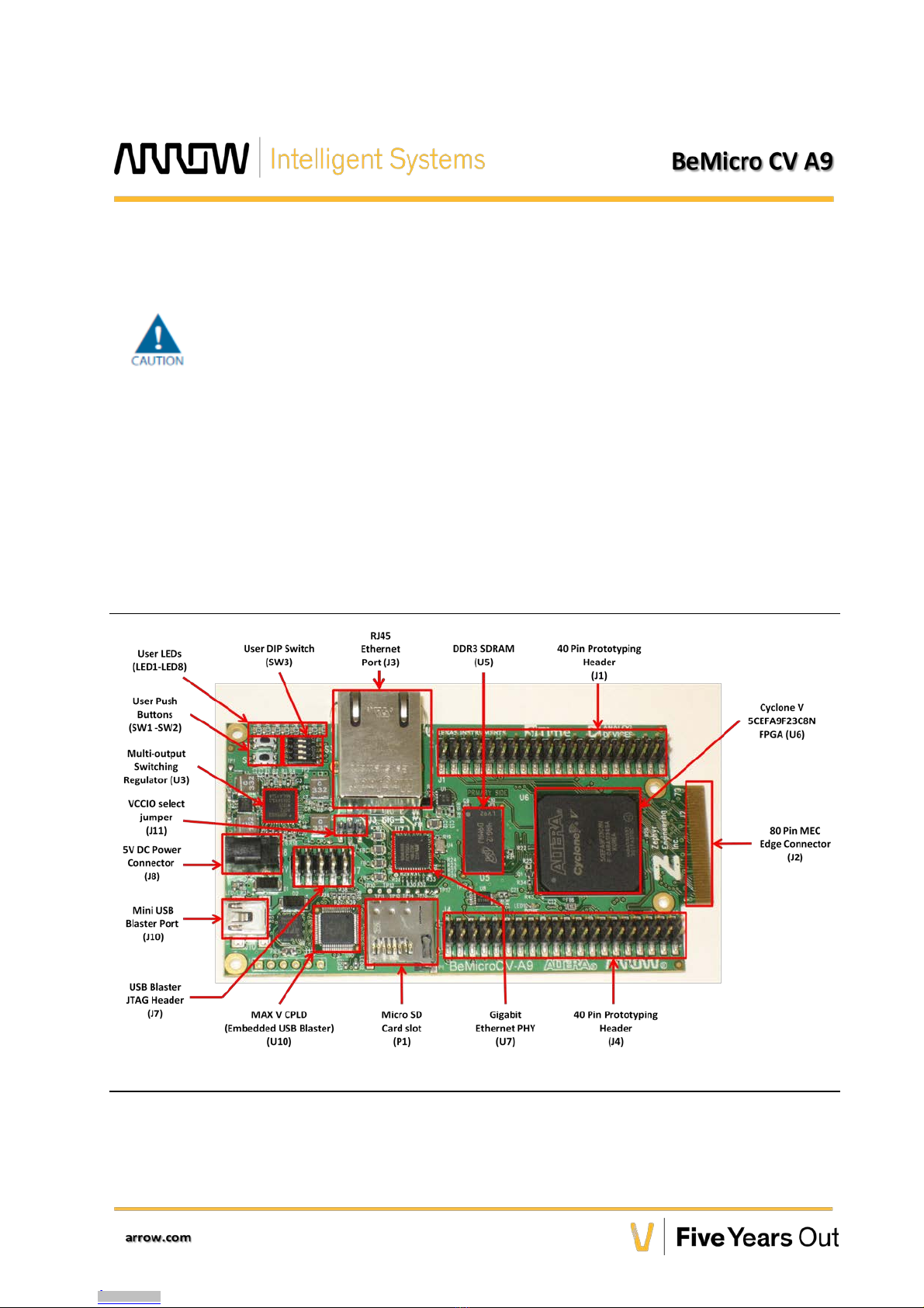
This document describes the hardware features of the BeMicro CV A9 Cyclone V E FPGA
Development Board, including component references and detailed pin-out information.
General Description
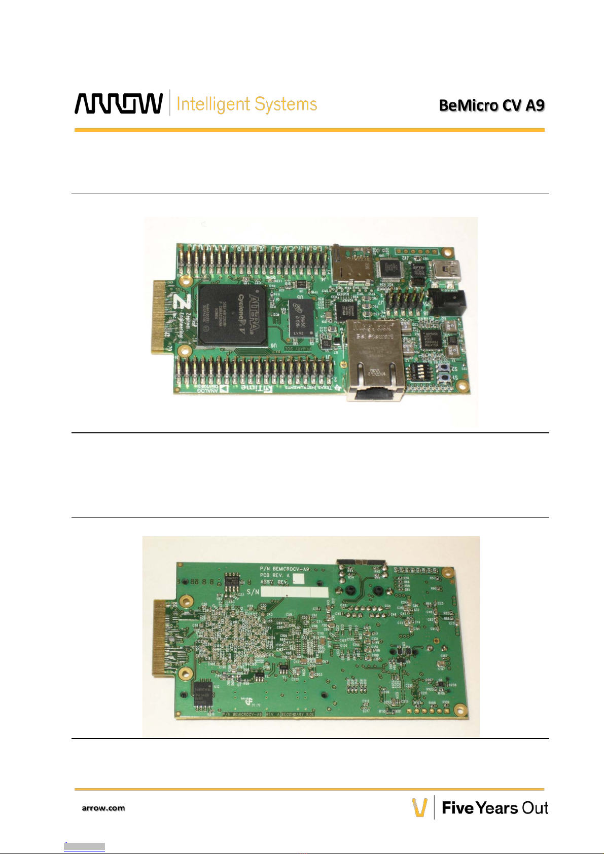
The Arrow Electronics BeMicro CV A9 is an enhanced BeMicro CV development board that
utilizes Altera’s 28-nm low-cost Cyclone V FPGA. It retains all the main features of the original
BeMicro CV predecessor while providing a higher logic density and additional features. The
5CEFA9F23C8N on the BeMicro CV A9 includes a hardened memory controller (HMC) connected
to a single 16-bit wide, 1Gb DDR3 SDRAM device. FPGA user I/O are routed to the two 40-pin
I/O headers and 80-pin MEC-style edge connector. The BeMicro CV A9 also includes an on
board USB Blaster programmer, Micro-SD card slot, and a 10/100/1000 Ethernet PHY.
The BeMicro CV A9 is well suited for DSP and logic-intensive applications such as Software
Defined Radio (SDR), data acquisition, and video processing. BeMicro CV A9 is compatible
with the Arrow BeScope digital oscilloscope, SDRstickTM SDR front-end boards, and the Terasic
MTL LCD module. For a complete list of products compatible with BeMicro CV A9 board, see
the BeMicro CV A9 Partner Pack at http://www.arrow.com/bemicro.
Users can easily migrate existing designs from BeMicro SDK or BeMicro CV to BeMicro CV A9.
Table 1-1 provides a brief feature comparison of the Cyclone-based BeMicro development
boards.
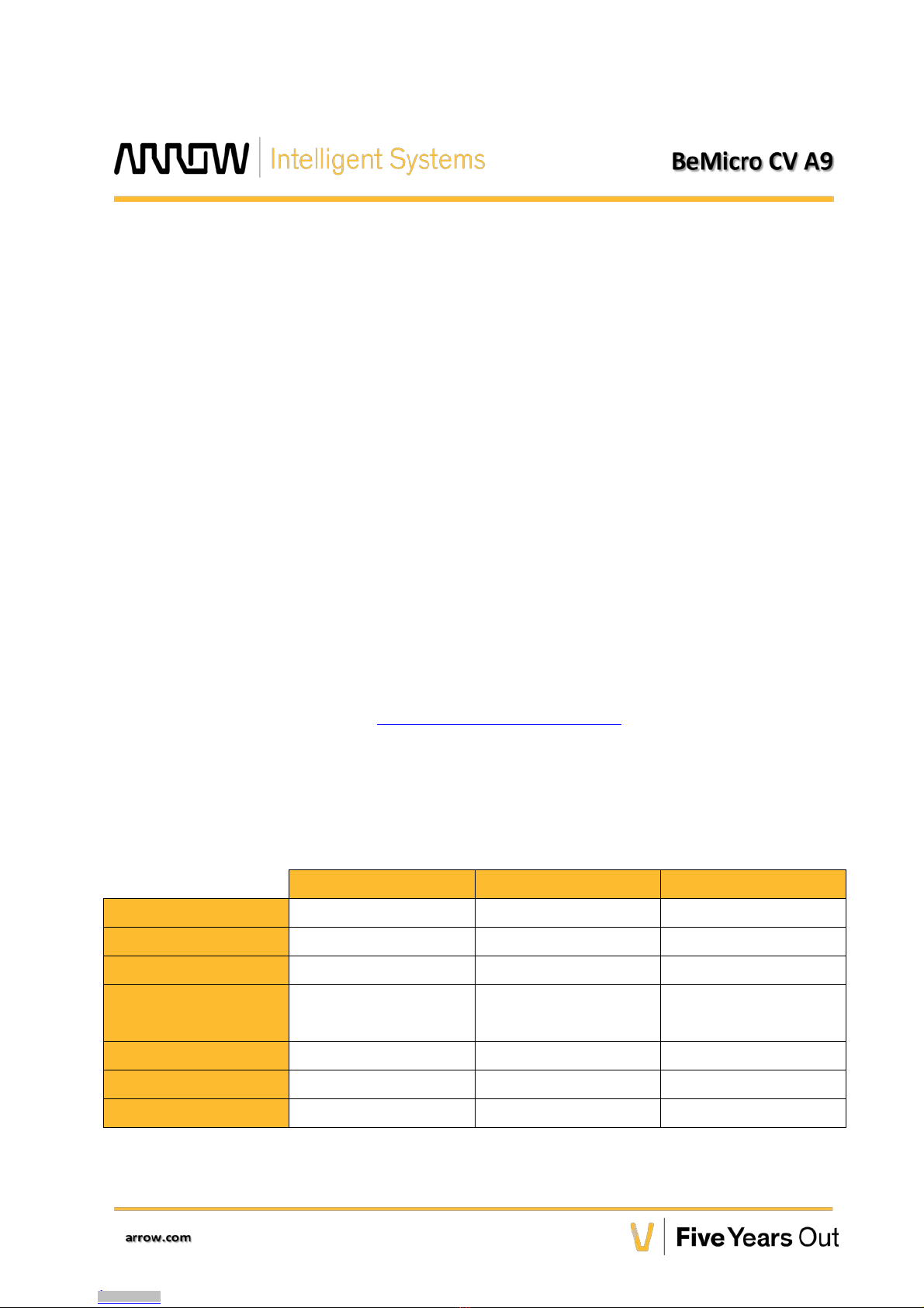
Table 1-1: BeMicro Feature Comparison
BeMicro SDK BeMicro CV BeMicro CV A9
FPGA EP4CE22F17C7 5CEFA2F23C8N 5CEFA9F23C8N
External Memory Mobile DDR DDR3 DDR3
Memory Controller Soft (Microtronix) Hard Hard
Expansion I/O 80 pin edge connector 2 x 40 pin I/O +
80 pin edge connector
2 x 40 pin I/O +
80 pin edge connector
Ethernet Yes No Yes
USB Blaster Integrated Integrated Integrated
Micro-SD card slot Yes Yes Yes
3
Downloaded from Arrow.com.Downloaded from Arrow.com.Downloaded from Arrow.com.

Board Component Features
The BeMicro CV A9 board features the following major component blocks:
Cyclone V E FPGA (5CEFA9F23C8N) in a 484-pin FineLine BGA (FBGA)
•113,560 adaptive logic modules (ALMs) equivalent to 301,000 LEs
•12,200 Kbit (Kb) M10K and 1,717 Kb MLAB memory
•8 fractional phase locked loops (PLLs)
•684 18 x 18-bit multipliers
•2 Hard Memory Controllers
•up to 480 general purpose input/output (GPIO)
•1.1 V core voltage
FPGA configuration circuitry
•256Mb QSPI Active Serial (AS) x4 configuration
•Embedded USB-BlasterTM II for use with the Quartus®II Programmer
•Separate JTAG configuration header
High Speed Networking
•Gigabit Ethernet PHY (Micrel KSZ9021)
•RJ-45 Ethernet connector
Clocking circuitry
•50 MHz 1.8V oscillator
•24 MHz 2.5V/3.3V oscillator
Memory
•1Gbit DDR3 SDRAM (64M x 16)
•1Kbit (128 x 8) two-wire Serial EEPROM
•Micro-SD card slot
General user input / output
•8 user LEDs
•2 user pushbuttons
•4 user DIP switches
Prototyping
•2 Terasic 40 pin prototyping headers (45 user I/O)
•BeMicro SDK 80-pin MEC card edge connector (57 user I/O)
Power via external 5V supply, or via USB for limited functions
4
Downloaded from Arrow.com.Downloaded from Arrow.com.Downloaded from Arrow.com.Downloaded from Arrow.com.

Figure 1-2 shows a top view of the BeMicro CV A9 FPGA development board.
Figure 1-2: Top View of BeMicro CV A9 Development Board.
Figure 1-3 shows a bottom view of the BeMicro CV A9 FPGA development board.
Figure 1-3: Bottom View BeMicro CV A9 Development Board
6
Downloaded from Arrow.com.Downloaded from Arrow.com.Downloaded from Arrow.com.Downloaded from Arrow.com.Downloaded from Arrow.com.Downloaded from Arrow.com.

Handling the Board
When handling the board, it is important to observe the following static discharge precaution:
Without proper anti-static handling, the board can be damaged. Therefore, use anti-static
handling precautions when touching the board.
2. Board Components
This chapter introduces the major components on the Be Micro CV A9 FPGA development
board. Figure 2-1 and Figure 2-2 illustrate the component locations.
Figure 2-1: Major component locations, Top View
7
Downloaded from Arrow.com.Downloaded from Arrow.com.Downloaded from Arrow.com.Downloaded from Arrow.com.Downloaded from Arrow.com.Downloaded from Arrow.com.Downloaded from Arrow.com.

Figure 2-2: Major component locations, Bottom View
This chapter includes the following sections:
•Cyclone V E FPGA
•Configuration Options
•Clock Circuitry
•General User Input / Output
•DDR3 Memory
•Ethernet Interface
•EEPROM
•Micro SD Card
•40 Pin Prototyping Headers
•80 Pin Card Edge Connector
•Power Supply
8
Downloaded from Arrow.com.Downloaded from Arrow.com.Downloaded from Arrow.com.Downloaded from Arrow.com.Downloaded from Arrow.com.Downloaded from Arrow.com.Downloaded from Arrow.com.Downloaded from Arrow.com.

Cyclone V E FPGA
The BeMicro CV A9 FPGA development board features a Cyclone V E FPGA device
(5CEFA9F23C8N) in a 484-pin FBGA package. Table 2–1 describes the features of the Cyclone
V E FPGA 5CEFA9F23C8N device.
Table 2-1: Features of the Cyclone V E 5CEFA9F23C8N
ALMs Equivalent
LE’s
M10K RAM
(Kbits)
MLAB RAM
(Kbits)
18-bit x 18-bit
Multipliers PLLs Package Type
113,560 301K 12,200 1,717 684 8 484 pin FBGA
Configuration Options
The BeMicro CV A9 FPGA development board supports the following configuration methods:
■Embedded USB-Blaster is the default method for configuring the FPGA using the
Quartus II Programmer in JTAG mode with the supplied USB cable.
■Active Serial Configuration via the on-board N25Q256A13EF8 configuration device.
FPGA Programming over Embedded USB-Blaster II
This configuration method combines a USB mini-B connector (J10), a USB 2.0 PHY device (U9),
and an Altera MAX V 5M80ZE64 CPLD (U10) to allow FPGA configuration using a USB cable.
This USB cable connects directly between the USB mini-B connector on the board and a USB
port on a PC running the Quartus II software. The embedded USB-Blaster in the MAX V
EPM80ZE64 CPLD normally masters the JTAG chain.
FPGA Programming using EPCQ Compatible Configuration PROM
The low-cost N25Q256A13EF8 non-volatile configuration PROM features a simple six-pin
interface and a small form factor. The PROM supports the AS x4 configuration mode. By
default, the BeMicro CV A9 board is set up to configure via AS x 4 configuration mode.
Resistors R97 and R98 allow selection between AS Fast and AS Standard modes.Figure 2–3
shows the connection between the EPCQ configuration device and the Cyclone V E FPGA.
9
Downloaded from Arrow.com.Downloaded from Arrow.com.Downloaded from Arrow.com.Downloaded from Arrow.com.Downloaded from Arrow.com.Downloaded from Arrow.com.Downloaded from Arrow.com.Downloaded from Arrow.com.Downloaded from Arrow.com.

Figure 2-3: Active Serial x4 Configuration Interface
Clock Circuitry
The development board includes two oscillators with frequencies of 24 MHz and 50 MHz.
Table 2–2 lists the oscillators, their I/O standard, and voltages required for the development
board.
Table 2-2: BeMico CV On-board oscillators
Board
Reference
Schematic Signal
Name
Frequency I/O
Standard
FPGA Pin
Number
Application
Y1 DDR3_CLK_50MHZ 50 MHz 1.8V H13 DDR3 HMC Clock Input
Y2 CLK_24MHZ 24 MHz 2.5V or
3.3V 1
M9 General Purpose Clock
Input, also used by
on-board USB Blaster II
Note 1: I/O voltage for this interface is selectable using the VCCIO_SEL jumper
General User Input / Output
The development board includes switches for user input and LEDs for status output. This
section describes these elements.
LED Outputs
There are multiple LED indicators on the board, but only LED1-LED8 are available for use
through FPGA I/O. Driving the FPGA output to a logic 0 will illuminate the LED. Driving a
logic 1 turns it off. Table 2–3 lists the LED board references, schematic signal names, and
functional descriptions.
10
Downloaded from Arrow.com.Downloaded from Arrow.com.Downloaded from Arrow.com.Downloaded from Arrow.com.Downloaded from Arrow.com.Downloaded from Arrow.com.Downloaded from Arrow.com.Downloaded from Arrow.com.Downloaded from Arrow.com.Downloaded from Arrow.com.

Table 2-3: LED Board Reference Information
Board
Reference
FPGA Pin
Number
Schematic Signal
Name
I/O
Standard
Functional
Description
LED1 B17 USER_LED1 1.5 V Green User LED
LED2 E19 USER_LED2 1.5 V Green User LED
LED3 E21 USER_LED3 1.5 V Green User LED
LED4 B21 USER_LED4 1.5 V Green User LED
LED5 C20 USER_LED5 1.5 V Green User LED
LED6 C21 USER_LED6 1.5 V Green User LED
LED7 D19 USER_LED7 1.5 V Green User LED
LED8 D21 USER_LED8 1.5 V Green User LED
LED9 NA NA NA ADP5052 Power
Good
LED10 NA DONE_N NA FPGA CONF_DONE
LED11 NA PWRON NA 5V DC In Power Good
LED12 NA USB_BLASTER_LED12 NA Green USB Blaster
Status
LED13 NA USB_BLASTER_LED13 NA Green USB Blaster
Status
User-Defined Push Buttons
Board references S1 and S2 are available for user-defined discrete input. Pressing and holding
down the switch will set the FPGA input pin to logic 0. Releasing the switch will set it to logic 1.
There are no board-specific functions for these general user push buttons. Table 2–4 lists the
user-defined push button schematic signal names and their corresponding Cyclone V E FPGA
pin numbers.
Table 2-4: User-defined Push-button Board Reference Information
Board Reference FPGA Pin Number Schematic Signal Name I/O Standard
S1 H18 TACT1 1.5V
S2 J18 TACT2 1.5V
11
Downloaded from Arrow.com.Downloaded from Arrow.com.Downloaded from Arrow.com.Downloaded from Arrow.com.Downloaded from Arrow.com.Downloaded from Arrow.com.Downloaded from Arrow.com.Downloaded from Arrow.com.Downloaded from Arrow.com.Downloaded from Arrow.com.Downloaded from Arrow.com.

User-Defined DIP Switch
Board reference SW3 is a 4-place DIP switch. This switch is user-defined and provides
additional FPGA input control. When the switch is in the OFF position, a logic 1 is selected.
When the switch is in the ON position, a logic 0 is selected. There are no board-specific
functions for this switch. Table 2–5 lists the user-defined DIP switch schematic signal names
and their corresponding Cyclone V E FPGA pin numbers.
Table 2-5: User-defined DIP Switch Board Reference Information
Board Reference FPGA Pin Number Schematic Signal Name I/O Standard
S3 C16 DIP_SW1 1.5V
S3 D17 DIP_SW2 1.5V
S3 G17 DIP_SW3 1.5V
S3 E16 DIP_SW4 1.5V
DDR3 Memory
The development board features a single 1 Gb (64 M x 16) DDR3 device. The device is
connected to the Cyclone V E FPGA so that the internal Hard Memory Controller (HMC) can be
used. The Cyclone V E FPGA speedgrade will determine the maximum speed at which the
DDR3 can be accessed as shown in Table 2–6.
Table 2-6: Hard Memory Controller Maximum Frequency of Operation
Temperature and
Speed Grade
Maximum Frequency
of Controller (MHz)
C6 400
C7 333
C8 333
I7 400
Table 2–7 lists the DDR3 pin assignments, signal names, and functions. The signal names and
types are relative to the Cyclone V E FPGA in terms of I/O setting and direction.
12
Downloaded from Arrow.com.Downloaded from Arrow.com.Downloaded from Arrow.com.Downloaded from Arrow.com.Downloaded from Arrow.com.Downloaded from Arrow.com.Downloaded from Arrow.com.Downloaded from Arrow.com.Downloaded from Arrow.com.Downloaded from Arrow.com.Downloaded from Arrow.com.Downloaded from Arrow.com.

Table 2-7: DDR3 pin assignments, signal names, and functions
FPGA Pin
Number
Schematic Signal
Name I/O Standard Description
L7 DDR3_A0 1.5V SSTL Class I Address bus
K7 DDR3_A1 1.5V SSTL Class I Address bus
H8 DDR3_A2 1.5V SSTL Class I Address bus
G8 DDR3_A3 1.5V SSTL Class I Address bus
J7 DDR3_A4 1.5V SSTL Class I Address bus
J8 DDR3_A5 1.5V SSTL Class I Address bus
A10 DDR3_A6 1.5V SSTL Class I Address bus
A9 DDR3_A7 1.5V SSTL Class I Address bus
A8 DDR3_A8 1.5V SSTL Class I Address bus
A7 DDR3_A9 1.5V SSTL Class I Address bus
C6 DDR3_A10 1.5V SSTL Class I Address bus
D6 DDR3_A11 1.5V SSTL Class I Address bus
D7 DDR3_A12 1.5V SSTL Class I Address bus
C8 DDR3_A13 1.5V SSTL Class I Address bus
A5 DDR3_BA0 1.5V SSTL Class I Bank address bus
B10 DDR3_BA1 1.5V SSTL Class I Bank address Bus
C9 DDR3_BA2 1.5V SSTL Class I Bank address bus
B6 DDR3_CASn 1.5V SSTL Class I Column address strobe
J9 DDR3_CLK_P Differential 1.5-V SSTL Class I Clock
H9 DDR3_CLK_N Differential 1.5-V SSTL Class I Clock
F14 DDR3_CKE 1.5V SSTL Class I Clock Enable
E9 DDR3_CSn 1.5V SSTL Class I Chip Select
G11 DDR3_DM0 1.5V SSTL Class I Data Mask
J17 DDR3_DM1 1.5V SSTL Class I Data Mask
E12 DDR3_DQ0 1.5V SSTL Class I Data bus bit 0, byte lane 0
D12 DDR3_DQ1 1.5V SSTL Class I Data bus bit 1, byte lane 0
C11 DDR3_DQ2 1.5V SSTL Class I Data bus bit 2, byte lane 0
K9 DDR3_DQ3 1.5V SSTL Class I Data bus bit 3, byte lane 0
C13 DDR3_DQ4 1.5V SSTL Class I Data bus bit 4, byte lane 0
D13 DDR3_DQ5 1.5V SSTL Class I Data bus bit 5, byte lane 0
13
Downloaded from Arrow.com.Downloaded from Arrow.com.Downloaded from Arrow.com.Downloaded from Arrow.com.Downloaded from Arrow.com.Downloaded from Arrow.com.Downloaded from Arrow.com.Downloaded from Arrow.com.Downloaded from Arrow.com.Downloaded from Arrow.com.Downloaded from Arrow.com.Downloaded from Arrow.com.Downloaded from Arrow.com.

B12 DDR3_DQ6 1.5V SSTL Class I Data bus bit 6, byte lane 0
F12 DDR3_DQ7 1.5V SSTL Class I Data bus bit 7, byte lane 0
F13 DDR3_DQ8 1.5V SSTL Class I Data bus bit 8, byte lane 1
E14 DDR3_DQ9 1.5V SSTL Class I Data bus bit 9, byte lane 1
J11 DDR3_DQ10 1.5V SSTL Class I Data bus bit 10, byte lane 1
A13 DDR3_DQ11 1.5V SSTL Class I Data bus bit 11, byte lane 1
B15 DDR3_DQ12 1.5V SSTL Class I Data bus bit 12, byte lane 1
C15 DDR3_DQ13 1.5V SSTL Class I Data bus bit 13, byte lane 1
G15 DDR3_DQ14 1.5V SSTL Class I Data bus bit 14, byte lane 1
K16 DDR3_DQ15 1.5V SSTL Class I Data bus bit 15, byte lane 1
H11 DDR3_DQS_P0 Differential 1.5-V SSTL Class I Data Strobe
H14 DDR3_DQS_P1 Differential 1.5-V SSTL Class I Data Strobe
G12 DDR3_DQS_N0 Differential 1.5-V SSTL Class I Data Strobe
J13 DDR3_DQS_N1 Differential 1.5-V SSTL Class I Data Strobe
L8 DDR3_ODT 1.5V SSTL Class I On Die Termination Control
B7 DDR3_RASn 1.5V SSTL Class I Row Address Strobe
J19 DDR3_RESETn LVCMOS15 Reset in
F7 DDR3_WEn 1.5V SSTL Class I Write Enable
Ethernet Interface
The BeMicro CV A9 board includes a Micrel KSZ9021 10/100/1000 Ethernet PHY and RJ45
connector. Altera’s Triple Speed Ethernet MAC soft IP core can be implemented inside the
Cyclone V FPGA to connect to the PHY through its RGMII interface.
Table 2-8: Ethernet PHY pin assignments, signal names, and functions
FPGA Pin
Number Schematic Signal Name I/O Standard Description
M8 ENET_RX_CLK 2.5 V or 3.3 V
1
RGMII RX Clock Output from PHY
L22 ENET_GTX_CLK 2.5 V or 3.3 V
1
RGMII TX Ref Clock Input to PHY
K21 ENET_RSTn 2.5 V or 3.3 V
1
Reset input to PHY
N8 ENET_INTn 2.5 V or 3.3 V
1
Interrupt Output from PHY
K22 ENET_TX_EN 2.5 V or 3.3 V
1
RGMII TX Control Input to PHY
V9 ENET_RX_DV 2.5 V or 3.3 V
1
RGMII RX Control Output from PHY
14
Downloaded from Arrow.com.Downloaded from Arrow.com.Downloaded from Arrow.com.Downloaded from Arrow.com.Downloaded from Arrow.com.Downloaded from Arrow.com.Downloaded from Arrow.com.Downloaded from Arrow.com.Downloaded from Arrow.com.Downloaded from Arrow.com.Downloaded from Arrow.com.Downloaded from Arrow.com.Downloaded from Arrow.com.Downloaded from Arrow.com.

V13 ENET_MDC 2.5 V or 3.3 V
1
Management Data Clock Input to PHY
AB12 ENET_MDIO 2.5 V or 3.3 V
1
Management Data I/O
M21 ENET_TXD0 2.5 V or 3.3 V
1
RGMII TX Data Input to PHY
M20 ENET_TXD1 2.5 V or 3.3 V
1
RGMII TX Data Input to PHY
N21 ENET_TXD2 2.5 V or 3.3 V
1
RGMII TX Data Input to PHY
N20 ENET_TXD3 2.5 V or 3.3 V
1
RGMII TX Data Input to PHY
AB6 ENET_RXD0 2.5 V or 3.3 V
1
RGMII RX Data Output from PHY
AB5 ENET_RXD1 2.5 V or 3.3 V
1
RGMII RX Data Output from PHY
AA7 ENET_RXD2 2.5 V or 3.3 V
1
RGMII RX Data Output from PHY
AB7 ENET_RXD3 2.5 V or 3.3 V
1
RGMII RX Data Output from PHY
Note 1: I/O voltage for this interface is selectable using the VCCIO_SEL jumper
EEPROM
The BeMicro CV A9 board includes a 1-Kb EEPROM device. This device has a 2-wire I2C serial
interface bus.Table 2–9 lists the EEPROM pin assignments, signal names and functions.
Table 2-9: EEPROM Board Reference Information
FPGA Pin Numbers Schematic Signal Name I/O Standard Description
P16 EEPROM_SDA 2.5 V or 3.3 V
1
Serial Data / Address
P17 EEPROM_SCL 2.5 V or 3.3 V
1
Serial Clock
Note 1: I/O voltage for this interface is selectable using the VCCIO_SEL jumper
Micro SD Card
The BeMicro CV A9 board includes a Micro SD card slot with x4 data interface to the FPGA.
Table 2–10 lists the FPGA pin assignments, signal names, and functions for the Micro SD card.
Table 2-10: Micro SD Card Board Reference Information
FPGA Pin Numbers Schematic Signal Name I/O Standard Description
M22 SDCLK 2.5 V or 3.3 V
1
SD Clock
W9 SDCMD 2.5 V or 3.3 V
1
SD Command Line
U6 SDD0 2.5 V or 3.3 V
1
SD Data bit 0
V6 SDD1 2.5 V or 3.3 V
1
SD Data bit 1
U7 SDD2 2.5 V or 3.3 V
1
SD Data bit 2
U8 SDD3 2.5 V or 3.3 V
1
SD Data bit 3
15
Downloaded from Arrow.com.Downloaded from Arrow.com.Downloaded from Arrow.com.Downloaded from Arrow.com.Downloaded from Arrow.com.Downloaded from Arrow.com.Downloaded from Arrow.com.Downloaded from Arrow.com.Downloaded from Arrow.com.Downloaded from Arrow.com.Downloaded from Arrow.com.Downloaded from Arrow.com.Downloaded from Arrow.com.Downloaded from Arrow.com.Downloaded from Arrow.com.

Note 1: I/O voltage for this interface is selectable using the VCCIO_SEL jumper
40 Pin Prototyping Headers
The BeMicro CV A9 board includes two 2×20 prototyping headers. The FPGA user I/O pins are
routed directly to the headers for design testing, debugging, verification and prototyping.
Table 2–11 and Table 2-12 summarize the debug header pin assignments, signal names, and
functions for 40 Pin Prototyping Headers J1 and J4, respectively.
Table 2-11: Board Reference Information for 40 Pin Prototyping Header J1
FPGA Pin Number Schematic Signal Name I/O Standard J1 Pin Number
NA NC NA 1
T15 GPIO2 2.5 V or 3.3 V
1
2
P22 GPIO3 2.5 V or 3.3 V
1
3
R15 GPIO4 2.5 V or 3.3 V
1
4
R22 GPIO5 2.5 V or 3.3 V
1
5
R16 GPIO6 2.5 V or 3.3 V
1
6
R21 GPIO7 2.5 V or 3.3 V
1
7
R17 GPIO8 2.5 V or 3.3 V
1
8
T22 GPIO1 2.5 V or 3.3 V
1
9
AA9 GPIO_D 2.5 V or 3.3 V
1
10
NA VCC5P0 NA 11
NA GND NA 12
T19 DIFF_TX_P9 2.5 V or 3.3 V
1
13
T20 DIFF_TX_N9 2.5 V or 3.3 V
1
14
AA8 LVDS_TX_O_N3 2.5 V or 3.3 V
1
15
AB8 LVDS_TX_O_P3 2.5 V or 3.3 V
1
16
Y11 LVDS_TX_O_N0 2.5 V or 3.3 V
1
17
AA12 LVDS_TX_O_P0 2.5 V or 3.3 V
1
18
NA NC NA 19
NA NC NA 20
T18 DIFF_RX_P9 2.5 V or 3.3 V
1
21
16
Downloaded from Arrow.com.Downloaded from Arrow.com.Downloaded from Arrow.com.Downloaded from Arrow.com.Downloaded from Arrow.com.Downloaded from Arrow.com.Downloaded from Arrow.com.Downloaded from Arrow.com.Downloaded from Arrow.com.Downloaded from Arrow.com.Downloaded from Arrow.com.Downloaded from Arrow.com.Downloaded from Arrow.com.Downloaded from Arrow.com.Downloaded from Arrow.com.Downloaded from Arrow.com.

T17 DIFF_RX_N9 2.5 V or 3.3 V
1
22
L19 DIFF_RX_P8 2.5 V or 3.3 V
1
23
L18 DIFF_RX_N8 2.5 V or 3.3 V
1
24
K17 DIFF_RX_P7 2.5 V or 3.3 V
1
25
L17 DIFF_RX_N7 2.5 V or 3.3 V
1
26
N19 DIFF_RX_P6 2.5 V or 3.3 V
1
27
M18 DIFF_RX_N6 2.5 V or 3.3 V
1
28
NA VCC3P3 NA 29
NA GND NA 30
N16 DIFF_RX_P5 2.5 V or 3.3 V
1
31
M16 DIFF_RX_N5 2.5 V or 3.3 V
1
32
U10 DIFF_RX_P4 2.5 V or 3.3 V
1
33
T9 DIFF_RX_N4 2.5 V or 3.3 V
1
34
R9 DIFF_RX_P3 2.5 V or 3.3 V
1
35
T10 DIFF_RX_N3 2.5 V or 3.3 V
1
36
U12 DIFF_RX_P2 2.5 V or 3.3 V
1
37
U11 DIFF_RX_N2 2.5 V or 3.3 V
1
38
R11 DIFF_RX_P1 2.5 V or 3.3 V
1
39
R10 DIFF_RX_N1 2.5 V or 3.3 V
1
40
Note 1: I/O voltage for this interface is selectable using the VCCIO_SEL jumper
17
Downloaded from Arrow.com.Downloaded from Arrow.com.Downloaded from Arrow.com.Downloaded from Arrow.com.Downloaded from Arrow.com.Downloaded from Arrow.com.Downloaded from Arrow.com.Downloaded from Arrow.com.Downloaded from Arrow.com.Downloaded from Arrow.com.Downloaded from Arrow.com.Downloaded from Arrow.com.Downloaded from Arrow.com.Downloaded from Arrow.com.Downloaded from Arrow.com.Downloaded from Arrow.com.Downloaded from Arrow.com.

Table 2-12: Board Reference Information for 40 Pin Prototyping Header J4
FPGA Pin Number Schematic Signal Name I/O Standard J4 Pin Number
NA VCC3P3 NA 1
NA VCC3P3 NA 2
NA NC NA 3
NA NC NA 4
V10 GPIO_A 2.5 V or 3.3 V
1
5
P8 GPIO_B 2.5 V or 3.3 V
1
6
NA GND NA 7
NA GND NA 8
NA GND NA 9
NA GND NA 10
R7 LVDS_TX_E_N4 2.5 V or 3.3 V
1
11
P7 LVDS_TX_E_P4 2.5 V or 3.3 V
1
12
W8 LVDS_TX_E_N3 2.5 V or 3.3 V
1
13
NA NC NA 14
NA NC NA 15
NA NC NA 16
NA GND NA 17
NA GND NA 18
NA NC NA 19
NA NC NA 20
NA NC NA 21
NA NC NA 22
NA NC NA 23
NA NC NA 24
NA GND NA 25
NA GND NA 26
NA NC NA 27
NA NC NA 28
AA10 GPIO_C 2.5 V or 3.3 V
1
29
18
Downloaded from Arrow.com.Downloaded from Arrow.com.Downloaded from Arrow.com.Downloaded from Arrow.com.Downloaded from Arrow.com.Downloaded from Arrow.com.Downloaded from Arrow.com.Downloaded from Arrow.com.Downloaded from Arrow.com.Downloaded from Arrow.com.Downloaded from Arrow.com.Downloaded from Arrow.com.Downloaded from Arrow.com.Downloaded from Arrow.com.Downloaded from Arrow.com.Downloaded from Arrow.com.Downloaded from Arrow.com.Downloaded from Arrow.com.

NA NC NA 30
Y10 LVDS_TX_OCLK_N 2.5 V or 3.3 V
1
31
Y9 LVDS_TX_OCLK_P 2.5 V or 3.3 V
1
32
NA GND NA 33
NA GND NA 34
R12 LVDS_TX_O_N2 2.5 V or 3.3 V
1
35
P12 LVDS_TX_O_P2 2.5 V or 3.3 V
1
36
AB10 LVDS_TX_O_N1 2.5 V or 3.3 V
1
37
AB11 LVDS_TX_O_P1 2.5 V or 3.3 V
1
38
NA NC NA 39
NA NC NA 40
Note 1: I/O voltage for this interface is selectable using the VCCIO_SEL jumper
80 Pin Card Edge Connector
All BeMicro cards have an 80 Pin Card Edge Connector Interface. A subset of the FPGA user
I/O pins are routed to card edge connector J2 for use with compatible add-on cards.
CAUTION
The BeMicro Card Edge Connector is not a standard interface with regards to FPGA
connectivity. Ensure that any card you connect to the BeMicro 80 Pin Card Edge Connector
is intended for that particular BeMicro variant. For further guidance, consult the add-on
card’s documentation, along with the BeMicro CV A9 Schematic at
https://parts.arrow.com/item/detail/arrow-development-tools/bemicrocva9
Table 2–13 lists the card edge connector J2 pin assignments, signal names, and functions.
Table 2-13: Board Reference Information for Card Edge Connector J2
FPGA Pin Number Schematic Signal Name I/O Standard J2 Pin Number
NA VCC3P3 NA 1
NA VCC3P3 NA 2
U13 RESET_EXPn 2.5 V or 3.3 V
1
3
NA No Connect NA 4
W16 EG_P1 2.5 V or 3.3 V
1
5
19
Downloaded from Arrow.com.Downloaded from Arrow.com.Downloaded from Arrow.com.Downloaded from Arrow.com.Downloaded from Arrow.com.Downloaded from Arrow.com.Downloaded from Arrow.com.Downloaded from Arrow.com.Downloaded from Arrow.com.Downloaded from Arrow.com.Downloaded from Arrow.com.Downloaded from Arrow.com.Downloaded from Arrow.com.Downloaded from Arrow.com.Downloaded from Arrow.com.Downloaded from Arrow.com.Downloaded from Arrow.com.Downloaded from Arrow.com.Downloaded from Arrow.com.

N9 EG_P35 2.5 V or 3.3 V
1
6
V15 EG_P2 2.5 V or 3.3 V
1
7
P9 EG_P36 2.5 V or 3.3 V
1
8
AA13 EG_P3 2.5 V or 3.3 V
1
9
NA GND NA 10
AA14 EG_P4 2.5 V or 3.3 V
1
11
M7 EG_P37 2.5 V or 3.3 V
1
12
Y14 EG_P5 2.5 V or 3.3 V
1
13
M6 EG_P38 2.5 V or 3.3 V
1
14
AB15 EG_P6 2.5 V or 3.3 V
1
15
N6 EG_P39 2.5 V or 3.3 V
1
16
AA15 EG_P7 2.5 V or 3.3 V
1
17
P6 EG_P40 2.5 V or 3.3 V
1
18
Y15 EG_P8 2.5 V or 3.3 V
1
19
R5 EG_P41 2.5 V or 3.3 V
1
20
NA GND NA 21
NA GND NA 22
Y16 EG_P9 2.5 V or 3.3 V
1
23
R6 EG_P42 2.5 V or 3.3 V
1
24
AB17 EG_P10 2.5 V or 3.3 V
1
25
T7 EG_P43 2.5 V or 3.3 V
1
26
AA17 EG_P11 2.5 V or 3.3 V
1
27
T8 EG_P44 2.5 V or 3.3 V
1
28
Y17 EG_P12 2.5 V or 3.3 V
1
29
P14 EG_P45 2.5 V or 3.3 V
1
30
AB18 EG_P13 2.5 V or 3.3 V
1
31
NA GND NA 32
NA GND NA 33
R14 EG_P46 2.5 V or 3.3 V
1
34
AA18 EG_P14 2.5 V or 3.3 V
1
35
T12 EG_P47 2.5 V or 3.3 V
1
36
AA19 EG_P15 2.5 V or 3.3 V
1
37
T13 EG_P48 2.5 V or 3.3 V
1
38
20
Downloaded from Arrow.com.Downloaded from Arrow.com.Downloaded from Arrow.com.Downloaded from Arrow.com.Downloaded from Arrow.com.Downloaded from Arrow.com.Downloaded from Arrow.com.Downloaded from Arrow.com.Downloaded from Arrow.com.Downloaded from Arrow.com.Downloaded from Arrow.com.Downloaded from Arrow.com.Downloaded from Arrow.com.Downloaded from Arrow.com.Downloaded from Arrow.com.Downloaded from Arrow.com.Downloaded from Arrow.com.Downloaded from Arrow.com.Downloaded from Arrow.com.Downloaded from Arrow.com.
Other manuals for BeMicro CV A9
1
Table of contents
Other Arrow Motherboard manuals

Arrow
Arrow verical RENESAS YSTREAM-IT-RZ-V2 User manual

Arrow
Arrow CYC1000 User manual

Arrow
Arrow MAX1000 User manual

Arrow
Arrow BeMicro CV A9 Operating and maintenance manual

Arrow
Arrow BeMicro Max 10 User manual

Arrow
Arrow einfochips eragon 660 User manual

Arrow
Arrow DC333A User manual

Arrow
Arrow verical LINEAR TECHNOLOGY DC1762A-A Quick setup guide

Arrow
Arrow Everest-CortexM1-SFP+Loop-Demo User manual

Arrow
Arrow CYC5000 User manual