Arrow CYC1000 User manual

CYC1000
User Guide
Please read the legal disclaimer at the end of this document.
Revision 1.0

CYC1000 User Guide www.arrow.com
Page | 2 January 2020
Table of Contents
Table of Figures ..................................................................................................................... 4
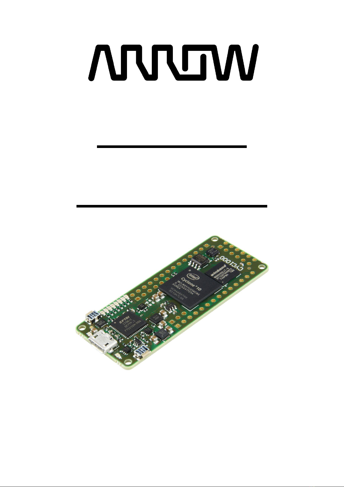
CYC1000 IoT / Maker Board.................................................................................. 5
1.1 About Arrow CYC1000 Board............................................................................................5
1.2 Useful Links.......................................................................................................................5
1.3 Getting Help......................................................................................................................6
Introduction to the CYC1000 Board ...................................................................... 7
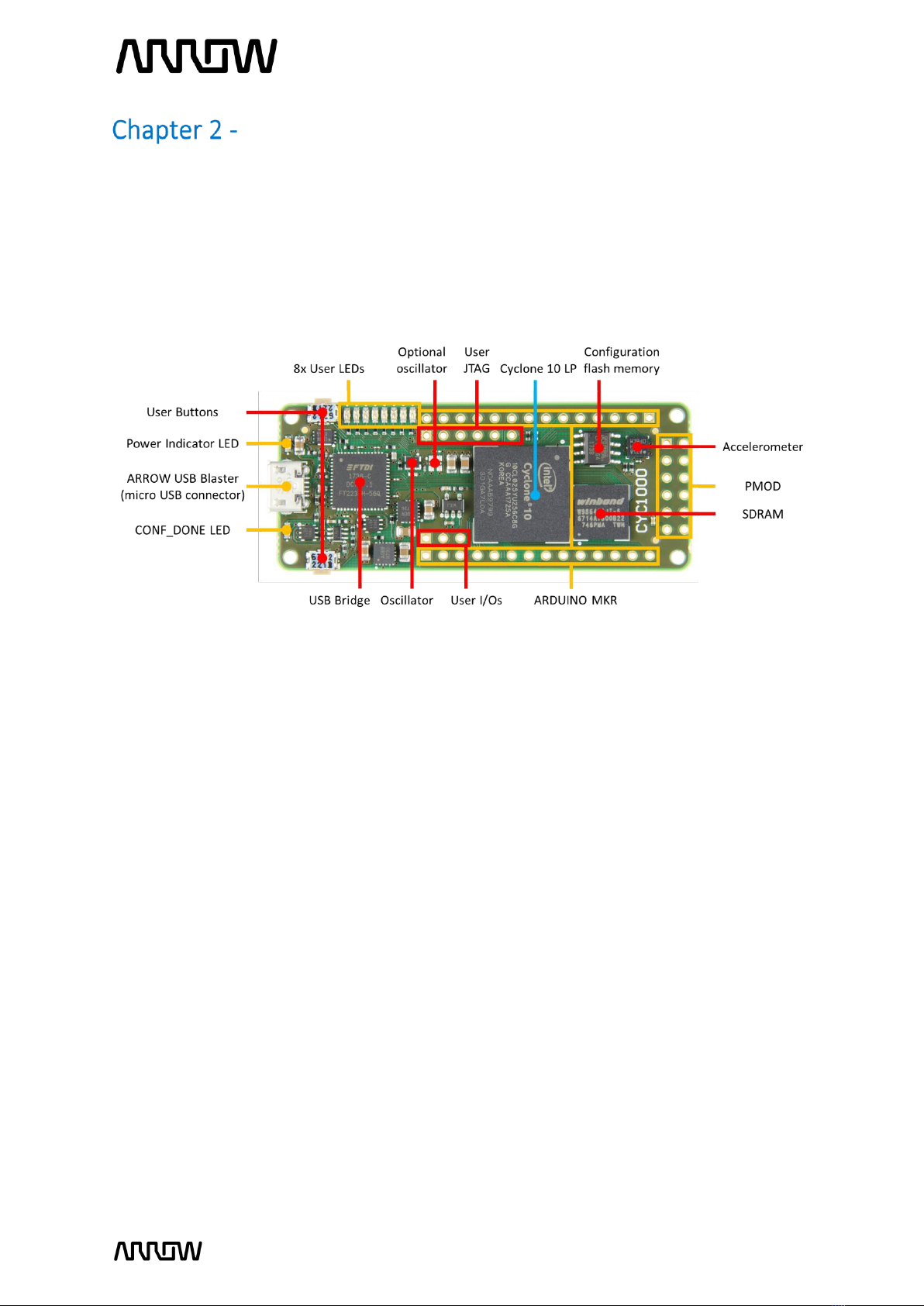
2.1 Layout and Components...................................................................................................7
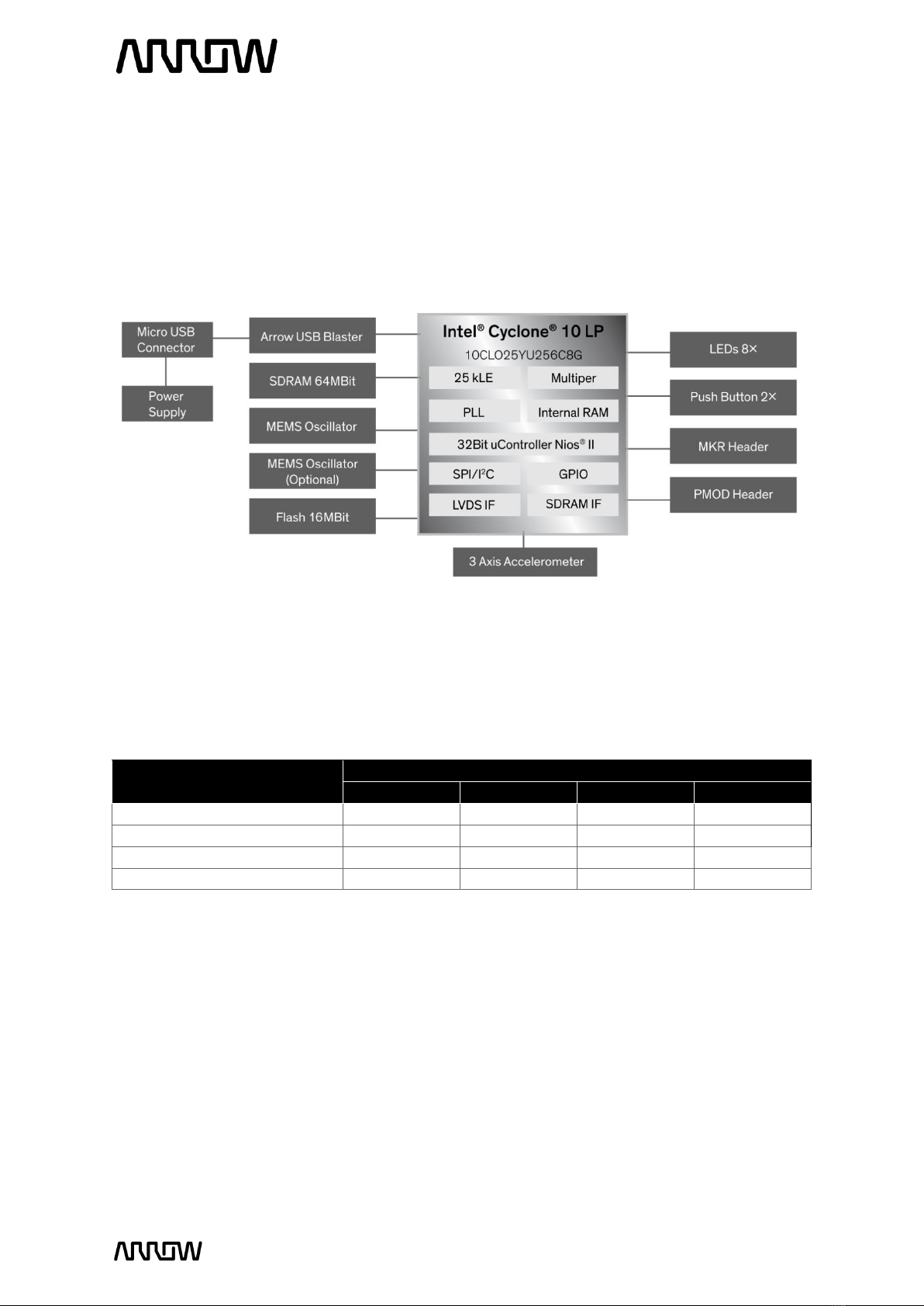
2.2 Block Diagram...................................................................................................................8
Connections and Peripherals of the CYC1000 Board............................................ 10
3.1 Board Status Elements....................................................................................................10
3.2 Clock Circuitry.................................................................................................................10
3.3 Peripherals Connected to the FPGA ...............................................................................11
3.3.1 LEDs.........................................................................................................................11
3.3.2 Push Buttons ...........................................................................................................12
3.3.3 Accelerometer.........................................................................................................12
3.3.4 SDRAM Memory......................................................................................................13
3.3.5 Serial Configuration Flash Memory ........................................................................14
3.3.6 Arduino MKR Connectors........................................................................................15
3.3.7 PMOD Connector ....................................................................................................16
3.3.8 User I/O...................................................................................................................17
3.3.9 Communication and Configuration.........................................................................17
3.3.10 Power Tree..............................................................................................................19
Software and Driver Installation......................................................................... 20
4.1 Installing Quartus Prime Software..................................................................................20
4.2 Installing Arrow USB Programmer2................................................................................21
New Project with CYC1000 ................................................................................. 24
5.1 Creating a new Blinky Project with CYC1000..................................................................24
5.2 Building a Blinky Project with CYC1000..........................................................................28
5.2.1 Block Diagram .........................................................................................................29
5.2.2 Components of the Design......................................................................................29
5.2.3 Catalog IP ................................................................................................................30
5.2.4 Create a PLL.............................................................................................................30
5.2.5 Create and Configure the PLL .................................................................................31

CYC1000 User Guide www.arrow.com
Page | 3 January 2020
5.2.6 Create and Configure the Counter..........................................................................34
5.2.7 Create and Configure the Multiplexer....................................................................36
5.2.8 Adding the Components to the Schematic.............................................................38
5.2.9 Connecting the Components ..................................................................................40
5.2.10 Add inputs, outputs to the schematic.....................................................................43
5.2.11 Analysis and Synthesis ............................................................................................46
5.2.12 Adding Timing Constraints......................................................................................46
5.2.13 Pinning Assignments ...............................................................................................48
5.2.14 Compiling the Design ..............................................................................................51
5.2.15 Reading the Compilation Report.............................................................................52
Configuring the CYC1000 .................................................................................... 54
6.1 Configure the FPGA in JTAG mode .................................................................................54
6.2 Serial configuration flash memory programming ..........................................................57
6.2.1 Programming File generation .................................................................................58
6.2.2 Device Programming...............................................................................................60
6.3 Testing the Design ..........................................................................................................62
Common Issues and Fixes................................................................................... 63
Appendix ........................................................................................................... 64
8.1 Revision History ..............................................................................................................64
8.2 Legal Disclaimer..............................................................................................................65

CYC1000 User Guide www.arrow.com
Page | 4 January 2020
Table of Figures
Figure 1 - CYC1000 Board (top view) ...............................................................................................7
Figure 2 - CYC1000 Block Diagram...................................................................................................8
Figure 3 –Position of Indication LEDs............................................................................................10
Figure 4 –CYC1000 Clock Tree.......................................................................................................10
Figure 5 –LED Connections............................................................................................................11
Figure 6 –Button Connections.......................................................................................................12
Figure 7 –Accelerometer Connections..........................................................................................12
Figure 8 –SDRAM Connections .....................................................................................................13
Figure 9 –Flash Connections .........................................................................................................14
Figure 10 - Arduino MKR Header Connections..............................................................................15
Figure 11 –PMOD Header Connections ........................................................................................16
Figure 12 - User I/O Connections...................................................................................................17
Figure 13 –UART Connections.......................................................................................................17
Figure 14 –JTAG Connections........................................................................................................18
Figure 15 –Power Tree Connections.............................................................................................19

CYC1000 User Guide www.arrow.com
Page | 5 January 2020
CYC1000 IoT / Maker Board
1.1 About Arrow CYC1000 Board
The CYC1000 is a customizable IoT / Maker Board ready for evaluation, development and/or use
in a product. It is built around the Intel Cyclone 10 LP FPGA, which is optimized for low-cost and
low-power, making them ideal for high-volume and cost-sensitive applications. High density sea
of programmable gates and on-board resources allow implementation of Nios II 32-bit
microcontroller IP, which provides the ideal solution for I/O expansion, chip-to-chip interfacing,
industrial, automotive and consumer applications.
The CYC1000 is equipped with an Arrow USB Programmer2, SDRAM, flash memory,
accelerometer sensor and PMOD/ADRUINO MKR connectors making it a fully featured plug and
play solution without any additional costs.
The CYC1000 board contains all the tools needed to use the board in conjunction with a computer
that runs a 64-bit Linux / Microsoft Windows 7 operating system or later.
1.2 Useful Links
A set of useful links that can be used to get relevant information about the CYC1000 or the Cyclone
10 LP FPGA.
•CYC1000 at Arrow Shop
•CYC1000 at Trenz Electronic Shop
•Intel Cyclone 10 LP Webpage
•CYC1000 Wiki Page

CYC1000 User Guide www.arrow.com
Page | 7 January 2020
Introduction to the CYC1000 Board
2.1 Layout and Components
Figure 1 shows a top view of the board. It depicts the layout of the board and indicates the location
of the various connectors and key components.
The following are available on the CYC1000 board:
•Intel Cyclone 10 LP 10CL025YU256C8G device
•Arrow USB Programmer2 on-board for programming; JTAG Mode
•64MBit SDRAM 166MHz
•16Mbit serial configuration flash memory
•12MHz MEMS Oscillator
•One optional MEMS Oscillator of preferred frequency
•8x red user LEDs
•2x board indication LEDs
•2x user push buttons
•3-axis accelerometer
•12-pin PMOD header
•Arduino MKR header
•User JTAG header
•User I/O header
Figure 1 - CYC1000 Board (top view)

CYC1000 User Guide www.arrow.com
Page | 8 January 2020
2.2 Block Diagram
Figure 2 represents the block diagram of the board. All the connections are established through
the Cyclone 10 LP FPGA device to provide maximum flexibility for users. Users can configure the
FPGA to implement any system design.
FPGA Device
•Available Cyclone 10 LP Devices for the CYC1000
Resources
Device
10CL006
10CL010
10CL016
10CL025
Logic Elements (LE)
6,272
10,320
15,408
24,624
M9K Memory (Kb)
270
414
504
594
18 x 18 Multiplier
15
23
56
66
PLLs
2
2
4
4
Configuration and Debug
•On-board Arrow USB Programmer2 (mini-USB type B connector)
Memory Devices
•4MBit to 32MBit external flash memory
•64MBit to 256MBit external SDRAM memory
Figure 2 - CYC1000 Block Diagram

CYC1000 User Guide www.arrow.com
Page | 9 January 2020
Headers
•PMOD Header
•Arduino MKR Header
•User JTAG Header
•User I/O Header
Buttons and Indicators
•2x side-buttons
•8x red user LEDs
•2x board indication LEDs
Sensors
•One 3-axis accelerometer
Power
•Recommended external supply voltage range: +5.0 V (nominal)
•Recommended I/O signal voltage range: 0 to +3.3 V

CYC1000 User Guide www.arrow.com
Page | 10 January 2020
Connections and Peripherals of the CYC1000 Board
3.1 Board Status Elements
In addition to the 8 LEDs that the FPGA can control, there are 2 additional LEDs which can indicate
the status of the board.
Board Reference
LED Name
Description
D1
3.3V
On when 3.3V power is active
D10
CONF_DONE
On when configuration data was loaded to Cyclone 10 LP
device without error
3.2 Clock Circuitry
All the external clocks of the system can be seen in Figure 4. The default clock (CLK12M) is at
12MHz and is connected and driving the FPGA’s user logic and the Arrow USB Programmer2.
There is an optional slot of another clock (CLK_X) to add another preferred clock source to the
FPGA. Both clocks are driving the internal PLLs.
For more information on clocks and PLLs of the Cyclone 10 LP, please refer to this document.
Figure 3 –Position of Indication LEDs
Figure 4 –CYC1000 Clock Tree

CYC1000 User Guide www.arrow.com
Page | 11 January 2020
Board Reference
FPGA Pin No.
Description
I/O Standard
CLK12M
PIN_M2
12MHz clock input
3.3 V
CLK_X
PIN_E15
Optional clock input
3.3 V
3.3 Peripherals Connected to the FPGA
3.3.1 LEDs
There are eight red user-controllable LEDs connected to the FPGA. Each LED is driven directly and
individually by the Cyclone 10 LP FPGA; driving its associated pin to a high logic level for on or low
logic level for off.
Board Reference
FPGA Pin No.
I/O Standard
LED1
PIN_M6
3.3 V
LED2
PIN_T4
3.3 V
LED3
PIN_T3
3.3 V
LED4
PIN_R3
3.3 V
LED5
PIN_T2
3.3 V
LED6
PIN_R4
3.3 V
LED7
PIN_N5
3.3 V
LED8
PIN_N3
3.3 V
Figure 5 –LED Connections

CYC1000 User Guide www.arrow.com
Page | 12 January 2020
3.3.2 Push Buttons
The board has two push buttons connected to the FPGA. Push buttons drive their associated pins
low logic level when pressed and high logic level when released.
Board Reference
FPGA Pin No.
Description
I/O Standard
RESET
PIN_H5
nCONFIG
3.3 V
USER_BTN
PIN_N6
User button
3.3 V
3.3.3 Accelerometer
The board comes with a digital accelerometer (LIS3DH), commonly known as the G-Sensor. This
G-Sensor is a small, thin, ultra-low power consumption, 3-axis accelerometer with digital I2C/SPI
serial interface, standard output. The LIS3DH has user-selectable full scales of +/-2g, +/-4g, +/-8g,
+/-16g and it is capable of measuring accelerations with output data rates from 1 Hz to 5 kHz. The
supplied power to the board (coming either from micro-USB connection or user Vin) can be
monitored through the ADC channel 3 of the accelerometer.
Figure 6 –Button Connections
Figure 7 –Accelerometer Connections

CYC1000 User Guide www.arrow.com
Page | 13 January 2020
Board Reference
FPGA Pin No.
Description
I/O Standard
SEN_INT1
PIN_B1
Interrupt 1
3.3 V
SEN_INT2
PIN_C2
Interrupt 2
3.3 V
SEN_SDI
PIN_G2
Data In (MOSI)*
3.3 V
SEN_SDO
PIN_G1
Data Out (MISO)*
3.3 V
SEN_SPC
PIN_F3
Clock*
3.3 V
SEN_CS
PIN_D1
Chip Select*
3.3 V
*For SPI connection
3.3.4 SDRAM Memory
The CYC1000 board supports 64MBit (default version) or up to 256MBit (customized version)
SDRAM which can operate up to 166 MHz clock frequency. Below are the connections and pinning
of the SDRAM used in the CYCX1000.
Board Reference
FPGA Pin No.
Description
I/O Standard
A0
PIN_A3
SDRAM Address [0]
3.3 V
A1
PIN_B5
SDRAM Address [1]
3.3 V
A2
PIN_B4
SDRAM Address [2]
3.3 V
A3
PIN_B3
SDRAM Address [3]
3.3 V
A4
PIN_C3
SDRAM Address [4]
3.3 V
A5
PIN_D3
SDRAM Address [5]
3.3 V
A6
PIN_E6
SDRAM Address [6]
3.3 V
A7
PIN_E7
SDRAM Address [7]
3.3 V
A8
PIN_D6
SDRAM Address [8]
3.3 V
A9
PIN_D8
SDRAM Address [9]
3.3 V
A10
PIN_A5
SDRAM Address [10]
3.3 V
A11
PIN_E8
SDRAM Address [11]
3.3 V
A12
PIN_A2
SDRAM Address [12]
3.3 V
A13
PIN_C6
SDRAM Address [13]
3.3 V
BA0
PIN_A4
SDRAM Bank Address [0]
3.3 V
BA1
PIN_B6
SDRAM Bank Address [1]
3.3 V
RAS
PIN_B7
SDRAM Row Address Strobe
3.3 V
CAS
PIN_C8
SDRAM Column Address Strobe
3.3 V
WE
PIN_A7
SDRAM Write Enable
3.3 V
CS
PIN_A6
SDRAM Chip Select
3.3 V
Figure 8 –SDRAM Connections

CYC1000 User Guide www.arrow.com
Page | 14 January 2020
Board Reference
FPGA Pin No.
Description
I/O Standard
CLK
PIN_B14
SDRAM Input Clock
3.3 V
CKE
PIN_F8
SDRAM Clock Enable
3.3 V
DQ0
PIN_B10
SDRAM Data [0]
3.3 V
DQ1
PIN_A10
SDRAM Data [1]
3.3 V
DQ2
PIN_B11
SDRAM Data [2]
3.3 V
DQ3
PIN_A11
SDRAM Data [3]
3.3 V
DQ4
PIN_A12
SDRAM Data [4]
3.3 V
DQ5
PIN_D9
SDRAM Data [5]
3.3 V
DQ6
PIN_B12
SDRAM Data [6]
3.3 V
DQ7
PIN_C9
SDRAM Data [7]
3.3 V
DQ8
PIN_D11
SDRAM Data [8]
3.3 V
DQ9
PIN_E11
SDRAM Data [9]
3.3 V
DQ10
PIN_A15
SDRAM Data [10]
3.3 V
DQ11
PIN_E9
SDRAM Data [11]
3.3 V
DQ12
PIN_D14
SDRAM Data [12]
3.3 V
DQ13
PIN_F9
SDRAM Data [13]
3.3 V
DQ14
PIN_C14
SDRAM Data [14]
3.3 V
DQ15
PIN_A14
SDRAM Data [15]
3.3 V
DQM0
PIN_B13
SDRAM Lower Data Mask
3.3 V
DQM1
PIN_D12
SDRAM Upper Data Mask
3.3 V
3.3.5 Serial Configuration Flash Memory
The CYC1000 board supports up to 32MBit of serial flash memory that can be used for user data
and programming non-volatile storage. The configuration bit stream is downloaded into the serial
configuration device which automatically loads the configuration data into the Cyclone 10 LP
when the board is powered on. Device memory capacity not consumed storing configuration data
can be used as general-purpose non-volatile memory, which is perfect for program and data
storage. Several interface peripherals available with Nios II embedded processors allow you to
access the serial configuration device as a memory module connected to your embedded system.
Figure 9 –Flash Connections

CYC1000 User Guide www.arrow.com
Page | 15 January 2020
Board Reference
FPGA Pin No.
Description
I/O Standard
AS_DATA
PIN_H2
Data In
3.3 V
AS_DCLK
PIN_H1
Clock
3.3 V
AS_NCS
PIN_D2
Chip Select
3.3 V
AS_ASDO
PIN_C1
Data Out
3.3 V
3.3.6 Arduino MKR Connectors
The CYC1000 board offers connectivity to Arduino MKR compatible shields that could also
alternatively be used as GPIOs. The MKR connectors offer up to 23 digital I/Os.
Board Reference
FPGA Pin No.
MKR Header
Description
I/O Standard
AREF
PIN_P11
J1/1
Input reference voltage or GPIO
3.3 V
AIN0
PIN_R12
J1/2
GPIO [0]
3.3 V
AIN1
PIN_T13
J1/3
GPIO [1]
3.3 V
AIN2
PIN_R13
J1/4
GPIO [2]
3.3 V
AIN3
PIN_T14
J1/5
GPIO [3]
3.3 V
AIN4
PIN_P14
J1/6
GPIO [4]
3.3 V
AIN5
PIN_R14
J1/7
GPIO [5]
3.3 V
AIN6
PIN_T15
J1/8
GPIO [6]
3.3 V
D0
PIN_N16
J1/9
Digital In [0]
3.3 V
D1
PIN_L15
J1/10
Digital In [1]
3.3 V
D2
PIN_L16
J1/11
Digital In [2]
3.3 V
D3
PIN_K15
J1/12
Digital In [3]
3.3 V
D4
PIN_K16
J1/13
Digital In [4]
3.3 V
D5
PIN_J14
J1/14
Digital In [5]
3.3 V
D6
PIN_N2
J2/1
Digital In [6]
3.3 V
D7
PIN_N1
J2/2
Digital In [7]
3.3 V
Figure 10 - Arduino MKR Header Connections

CYC1000 User Guide www.arrow.com
Page | 16 January 2020
Board Reference
FPGA Pin No.
MKR Header
Description
I/O Standard
D8
PIN_P2
J2/3
Digital In [8]
3.3 V
D9
PIN_J1
J2/4
Digital In [9]
3.3 V
D10
PIN_J2
J2/5
Digital In [10]
3.3 V
D11
PIN_K2
J2/6
Digital In [11]*
3.3V
D12
PIN_L2
J2/7
Digital In [12]*
3.3 V
D13
PIN_P1
J2/8
Digital In [13]
3.3 V
D14
PIN_R1
J2/9
Digital In [14]
3.3 V
D11_R
PIN_K1
J2/6
Digital In [11] with resistor*
3.3 V
D12_R
PIN_L1
J2/7
Digital In [12] with resistor*
3.3 V
RESET
PIN_H5
J2/10
System reset of the board
3.3 V
GND
N/A
J2/11
Ground output to the connector
N/A
3.3V
N/A
J2/12
3.3V power to the connector
N/A
VIN
N/A
J2/13
User power into to the CYC1000
N/A
5V
N/A
J2/14
5V power to the connector
N/A
*Can only choose one, hence same name pinning
3.3.7 PMOD Connector
The CYC1000 board offers connectivity to PMOD compatible connectors (2x6-pin or 1x12-pin),
making it possible to add a big variety of sensors or ICs to the system. Below is the connection
schematic and pinning information.
Board Reference
FPGA Pin No.
Description
I/O Standard
PIO_01
PIN_F13
PMOD Pin 1
3.3 V
PIO_02
PIN_F15
PMOD Pin 2
3.3 V
PIO_03
PIN_F16
PMOD Pin 3
3.3 V
PIO_04
PIN_D16
PMOD Pin 4
3.3 V
PIO_05
PIN_D15
PMOD Pin 5
3.3 V
PIO_06
PIN_C15
PMOD Pin 6
3.3 V
PIO_07
PIN_B16
PMOD Pin 7
3.3 V
PIO_08
PIN_C16
PMOD Pin 8
3.3 V
GND
N/A
Ground
N/A
3.3V
N/A
3.3 V Power to PMOD
N/A
Figure 11 –PMOD Header Connections

CYC1000 User Guide www.arrow.com
Page | 17 January 2020
3.3.8 User I/O
The CYC1000 board has two additional pins that can be connected to the board and take GPIOs.
Board Reference
FPGA Pin No.
Description
I/O Standard
AIN
PIN_T12
GPIO
3.3 V
AIN7
PIN_R11
GPIO
3.3 V
GND
N/A
Ground
N/A
3.3.9 Communication and Configuration
The CYC1000 board uses a single chip to perform configuration of the device and USB to UART
communications, having each described below.
3.3.9.1 UART Communication
UART to USB communication supports USB 2.0 High Speed (up to 480 Mb/s) independently of
other protocols used in the chip like JTAG. Below is the connection schematic and pinning
information.
Board Reference
FPGA Pin No.
Description
I/O Standard
BDBUS0
PIN_R7
Transmitter output of FT2232H (Tx)
3.3 V
BDBUS1
PIN_T7
Receiver input of FT2232H (Rx)
3.3 V
BDBUS2
PIN_R6
Ready To Send handshake output (RTS)
3.3 V
BDBUS3
PIN_T6
Clear To Send handshake input (CTS)
3.3 V
BDBUS4
PIN_R5
Data Transmit Ready (DTR)
3.3 V
BDBUS5
PIN_T5
Data Set Ready (DSR)
3.3 V
Figure 12 - User I/O Connections
Figure 13 –UART Connections

CYC1000 User Guide www.arrow.com
Page | 18 January 2020
3.3.9.2 JTAG Chain Configuration
There are two types of configuration methods supported by CYC1000:
1. JTAG Configuration: configuration using JTAG ports. JTAG configuration scheme allows you to
directly configure the device core through JTAG pins (TDI, TDO, TMS and TCK pins). The
Quartus Prime software automatically generates a .sof that can be downloaded to the Cyclone
10 LP with a download cable through the Quartus Prime Programmer.
2. Configuration from EPCQ-A flash: configuration using external flash. Before configuration,
you need to program the configuration data .jic into the configuration flash memory (EPCQ-
A) which provides non-volatile storage for the bit stream. The information is retained within
EPCQ-A even if the CYC1000 is turned off. When the board is powered on, the configuration
data in the EPCQ-A is automatically loaded into the Cyclone 10 LP FPGA.
The FPGA device can be configured through JTAG interface on CYC1000, but the JTAG chain must
form a closed loop, which allows Quartus Prime programmer to detect the FPGA device.
CYC1000 offers two ways of configuring your board.
1) Through the on-board Arrow USB Programmer2
2) Pins for connecting user’s preferred JTAG interface
Board Reference
FPGA Pin No.
Description
I/O Standard
TCK
PIN_H3
Test Interface Clock
3.3 V
TDO
PIN_J4
Test Data Out
3.3 V
TDI
PIN_H4
Test Data In
3.3 V
TMS
PIN_J5
Test Mode Select
3.3 V
For detailed information about how to configure the Cyclone 10 LP, please refer to Chapter 6.
Figure 14 –JTAG Connections

CYC1000 User Guide www.arrow.com
Page | 19 January 2020
3.3.10 Power Tree
The CYC1000 is powered by Enpirion’s buck regulator, which provides high efficiency up to 1A
with integrated magnetics, switches, control, and compensation. As seen from the diagram
below, the board can be powered either by a micro-USB connection, or by user input voltage from
the Arduino MKR header (takes precedence over the USB bus). All devices are powered by 3.3V
voltage line and the 5V and 3.3V lines are fed back to the Arduino header to power that
connection if needed. The Cyclone 10 LP FPGA is powered by 2 Enpirion devices, while a Microchip
LDO provides auxiliary voltage.
Figure 15 –Power Tree Connections

CYC1000 User Guide www.arrow.com
Page | 20 January 2020
Software and Driver Installation
Firstly it is required to create your Basic Intel Account if you don’t own one already. It is required
to download the software. Below are guides for installing the software and drivers for Windows
operating systems.
4.1 Installing Quartus Prime Software
4.1.1 Go to the Intel Download Center: Link.
4.1.2 Select Windows as the operating system (highlighted in red).
4.1.3 Select Release 18.1, or your preferred version (highlighted in red).
4.1.4 Download the following files from the “Individual Files” tab (highlighted in yellow):
-Quartus Prime Lite Edition (Free)
-ModelSim-Intel FPGA Edition (includes Starter Edition)
-Cyclone 10 LP device support
4.1.5 Click on button to begin the download and save them in the same folder.
Table of contents
Other Arrow Motherboard manuals

Arrow
Arrow verical CYPRESS S6SBP201A1AVA1001 User manual

Arrow
Arrow einfochips eragon 660 User manual

Arrow
Arrow verical RENESAS YSTREAM-IT-RZ-V2 User manual

Arrow
Arrow CYC5000 User manual

Arrow
Arrow BeMicro Max 10 User manual

Arrow
Arrow DC333A User manual

Arrow
Arrow SD 600eval Instructions for use

Arrow
Arrow BeMicro CV A9 Operating and maintenance manual

Arrow
Arrow MAX1000 User manual

Arrow
Arrow verical LINEAR TECHNOLOGY DC1762A-A Quick setup guide