[AKD5704-C]
[KM137900] 2023/11
- 10 -
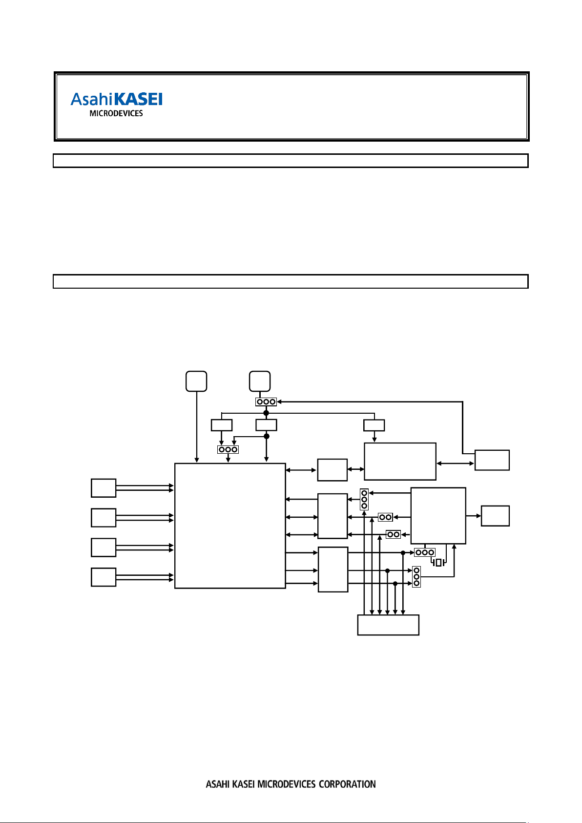
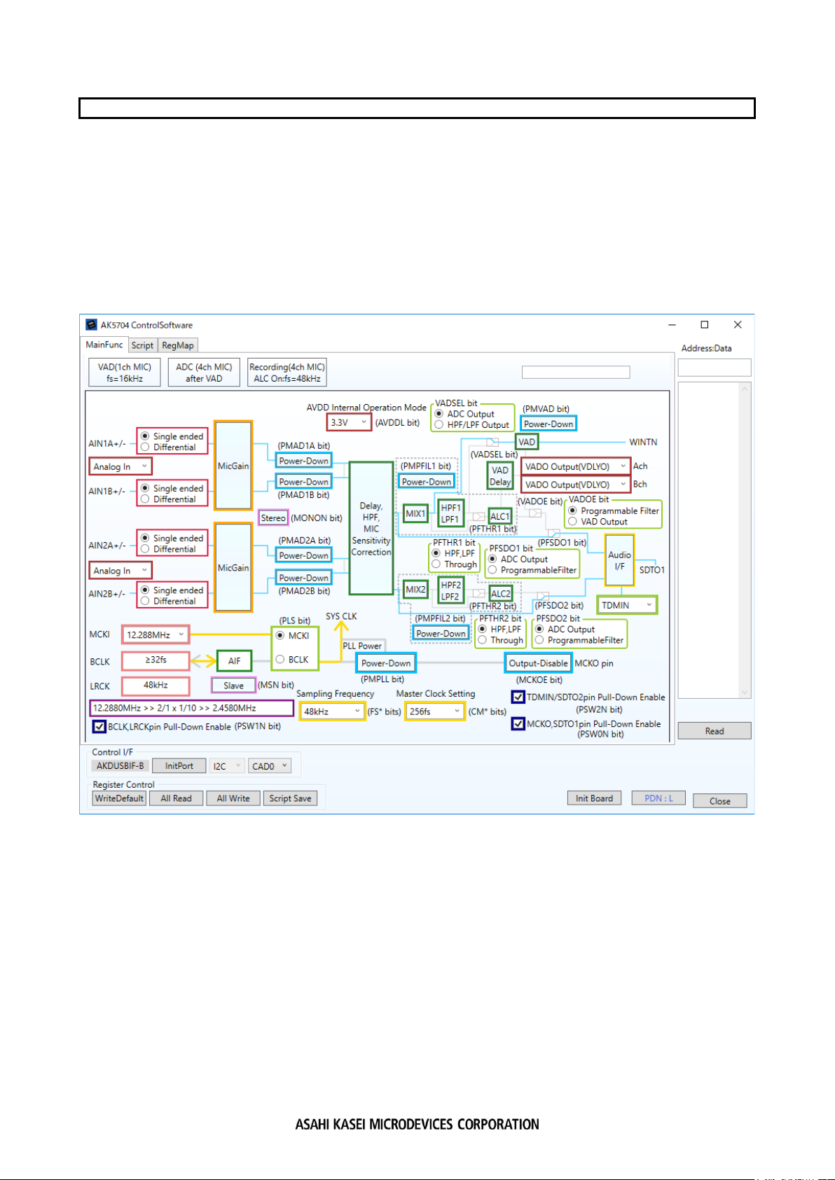
◼Tab Functions
(1) [MainFunc] Tab: Function Control
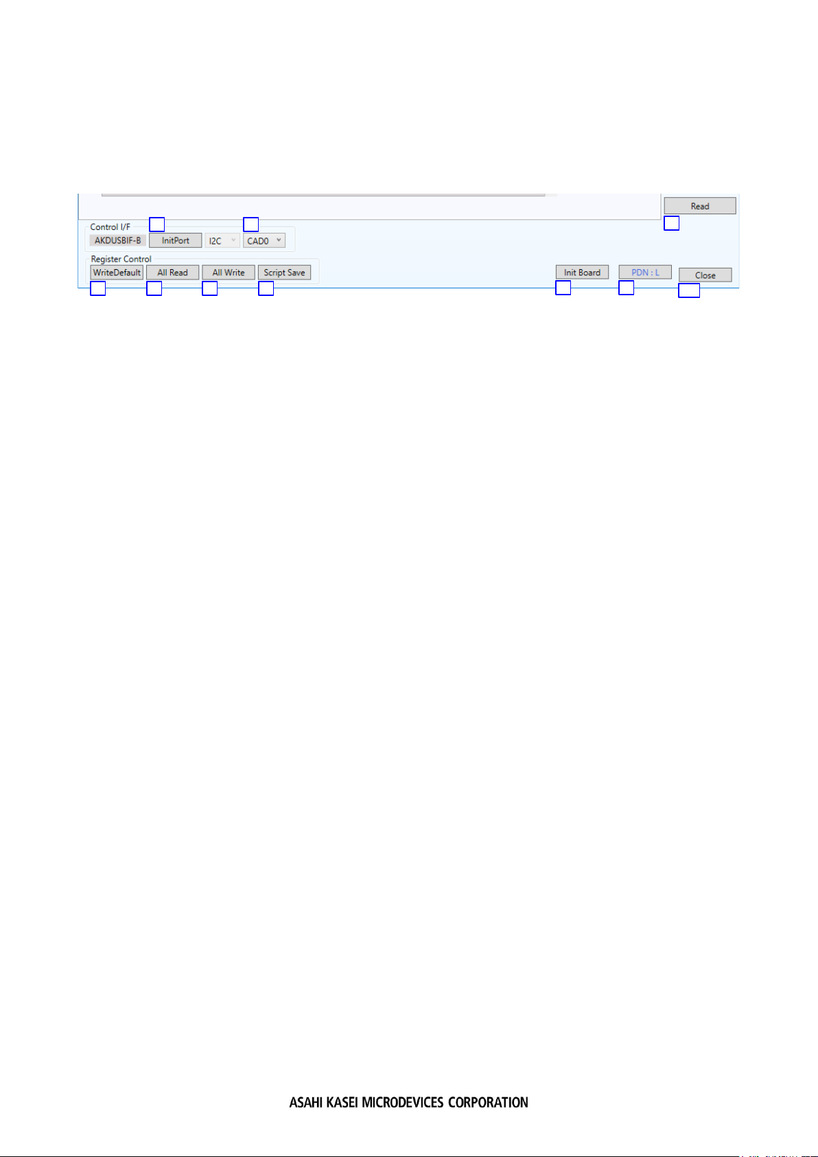
Clicking on each block in the window opens the settings window for that block. The displayed selector can be selected
directly. With the three function buttons at the top of the window, execute the sequence processing of the function
described on the button.
Figure 8. [MainFunc] Window
1. AVDD operation mode setting
2. Analog input/Digital microphone input select (AIN1, AIN2)
3. Single-ended input/Full-differential input select (AIN1A, AIN1B, AIN2A, AIN2B)
4. Stereo/Mono mode select
5. SDTO2 output, TDMIN input select
6. Slave/Master mode select
7. PLL clock source (MCKI/BCLK) select
8. MCKI frequency select
9. BCLK output frequency select (Only master mode)
10. Sampling Frequency select
11. Master clock rate select
12. Master clock output select
13. Pull-down resistance of each pin enable/disable (BCLK, LRCK, TDMIN/SDTO2, MCKO, SDTO1)
14. Power management of each block
(PMAD1A, PMAD1B, PMAD2A, PMAD2B, PMPFIL1, PMPFIL2, PMVAD, PMPLL)