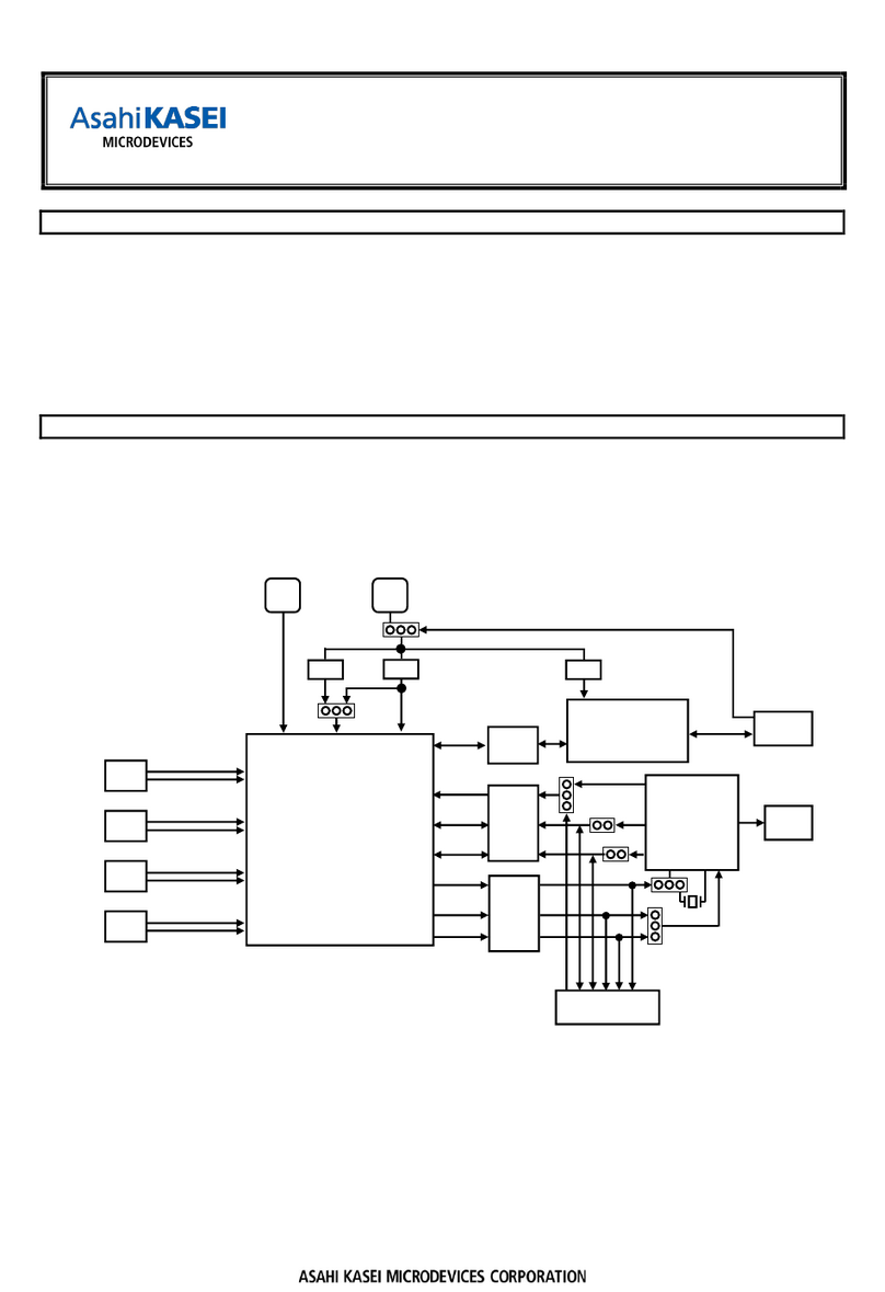
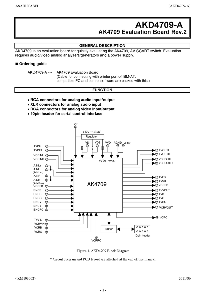
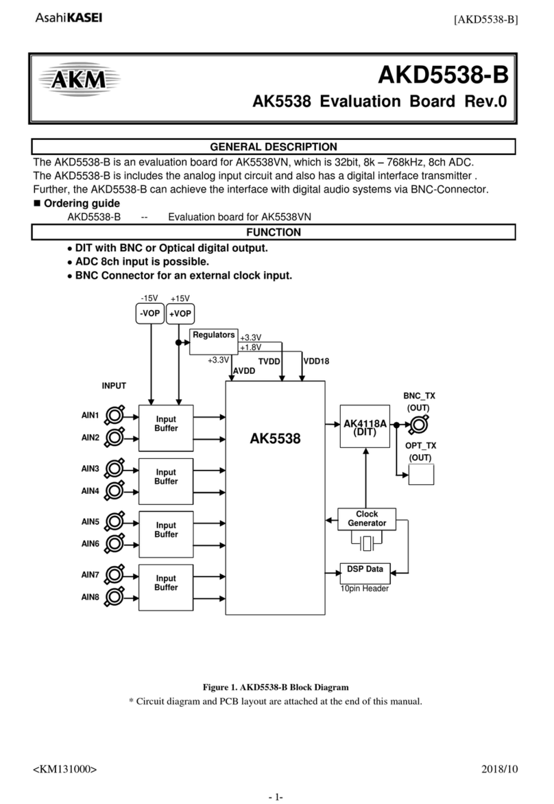
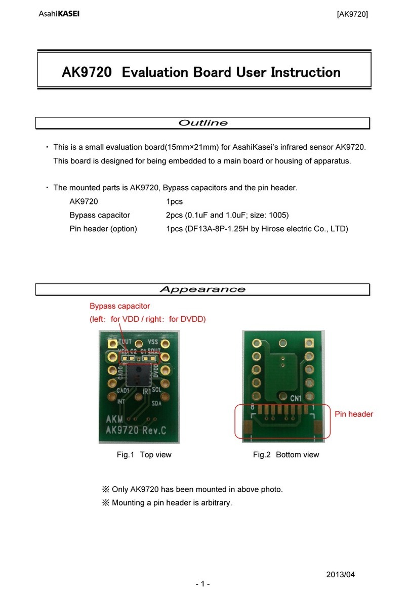
Asahi KASEI AKD4220-A User manual

[AKD4220-A]
<KM083401> 2012/04
- 1 -
GENERAL DESCRIPTION
AKD4220-A is an evaluation board for AK4220 that has various 7:3 audio and 6:3 video switches. This
board can achieve the interface with AV systems via RCA connectors.
Ordering guide
AKD4220-A ---AK4220 Evaluation Board
10-wire flat cable for connection with printer port of PC (IBM-AT compatible
machine), control software for AK4220, driver for control software on Windows
2000/XP are packed with this.
Control software does not work on Windows NT
Windows 2000/XP needs an installation of driver.
Windows 95/98/ME does not need an installation of driver.
FUNCTION
•RCA connectors for analog audio: 7 inputs 3 outputs
•RCA connectors for video: 6 inputs, 3 outputs
•10-pin header for I2C/4-wire serial control
AK4220
GND1 LOUT1
ROUT1
LOUT2
AVDD
LIN+1
RIN+1
LIN+2
GND3
LIN+3
GND2 ROUT2
+12V
VVDD1
DVDD
RIN+2
GND6
LIN+7
RIN+6
GND7
LIN+4
RIN+3
RIN+4
GND5
LIN+5
GND4
RIN+5
LIN+6
RIN+7
VIN3
VIN4
VIN5
VIN6
VIN1
VIN2
LOUT3
ROUT3
VOUT1
VOUT2
VOUT3
REG 5V
Digital Logic
D3.3V
Input
circuits
Output
circuits
VVDD2
AVDD VVDD1 D5V REG
3.3V
DVDD
Figure 1. AKD4220-A Block Diagram
* Circuit diagram and PCB layout are attached at the end of this manual.
AK4220 Evaluation Board Rev.0
A
KD4220-
A

[AKD4220-A]
<KM083401> 2012/04
- 2 -
EVALUATION BOARD MANUAL
Operation sequence
1) Set up power supply lines.
Name of
jack Color
of jack Voltage Used for Open / connect Default
Setting
+12V Green +12V Regulator (T1)
Should be always connected when
power supply lines are supplied from
regulator of T1. In this case “JP9
(REG)” is set to short.
+12V
AVDD Red +5V AVDD of AK4220 Should be always connected when
AVDD is not supplied from regulator
of T1. In this case “JP9 (REG)” is set to
open.
Open
VVDD1 Bule +5V VVDD1 of AK4220 Should be always connected when
AVDD is not supplied from regulator
of T1. In this case “JP10 (VVDD1)” is
set to open.
Open
D5V Red +5V Regulator (T2) Should be always connected when
JP2(DVDD_SEL) is set to DVDD side.
Can be open when JP2(DVDD_SEL) is
set to REG side.
Open
DVDD Orange +3.3V DVDD of AK4220 Should be always connected when
DVDD is not supplied from regulator
of T1 and T2. In this case “JP15
(DVDD)” is set to open.
Open
D3.3V Orange +3.3V Digital Logic Should be always connected when
D3.3V is not supplied from regulator of
T1 and T2. In this case “JP13 (D3.3V)”
is set to open.
Open
AGND Black 0V Analog Ground Should be always connected. 0V
VVSS Black 0V Analog Ground Should be always connected. 0V
DGND Black 0V Digital Ground Should be always connected, when JP1
(GND) is set to open. 0V
Table 1. Set up the power supply lines
(Note) Each supply line should be distributed from the power supply unit.
2) Set-up jumper pins and DIP switches. (See the followings.)
3) Power on.
AK4220 should be reset once bringing SW2 (PDN) to “L” upon power-up.

[AKD4220-A]
<KM083401> 2012/04
- 3 -
Set up jumper pins
1. JP1 (GND) : Analog ground and Digital ground
OPEN :Separated.
SHORT : Common. (The connector “DGND” can be open.) <Default>
2. JP9 (REG) : AVDD, VVDD1 of the AK4220, and regulator of T2 (TA48M033F)
OPEN : AVDD is supplied from “AVDD ” jack. (“+12V” jack should be open)
SHORT : AVDD is supplied from regulator of T1 (NJM78M05FA). < Default >
3. JP16 (AVDD) : AVDD of the AK4220
OPEN : AVDD is supplied from “AVDD ” jack.
SHORT : AVDD is supplied from regulator of T1 (NJM78M05FA).
(“AVDD” jack should be open) < Default >
4. JP10 (VVDD1) : VVDD1 of the AK4220
OPEN : VVDD1 is supplied from “VVDD1 ” jack.
SHORT : VVDD1 is supplied from regulator of T1 (NJM78M05FA).
(“VVDD1” jack should be open) < Default >
5. JP11 (D-A) : Regulator of T2 (TA48M033F)
OPEN : Regulator of T2 (TA48M033F) is supplied from “D5V ” jack.
SHORT : Regulator of T2 (TA48M033F) is supplied from regulator of T1 (NJM78M05FA).
(“D5V” jack should be open) < Default >
6. JP15 (DVDD) : DVDD of the AK4220
OPEN : DVDD is supplied from “DVDD ” jack.
SHORT : DVDD is supplied from regulator of Regulator of T2 (TA48M033F).
(“DVDD” jack should be open) < Default >
7. JP13 (D3.3V) : Power of digital logic
OPEN : D3.3V is supplied from “D3.3V ” jack.
SHORT : D3.3V is supplied from regulator of Regulator of T2 (TA48M033F).
(“D3.3V” jack should be open) < Default >
8. JP12 (VVDD2) : Should be open.

[AKD4220-A]
<KM083401> 2012/04
- 4 -
Set up DIP switches
SW1 Setting for I2C of AK4220
Pin No. Pin Name ON (“H”,“1”) / OFF (“L”,“0”) Default
1 I2C Control mode Select ON (“H”, “1”)
2 CAD1 Chip Address Select (Note1) OFF (“L”, “0”)
3 CAD0 Chip Address Select (Note1) OFF (“L”, “0”)
Table 2. SW1 Setting for I2C of AK4220
(Note1) Chip Address is selected by CAD1, CAD0 pin (CAD10=”00”,”01”,”10”,”11”)
The function of the toggle SW
[SW2] (PDN): Resets the AK4220. Keep “H” during normal operation.
Indication for LED
[LE1] (INT): Monitor INT0 pin of the AK4220. LED turns on when channel dependent audio input detect
circuit and video signal detect circuit of the AK4220.
[LE2 ∼6] (Q0 ∼4): Monitor Q0 ∼4 pin of the AK4220.

[AKD4220-A]
<KM083401> 2012/04
- 5 -
Serial Control
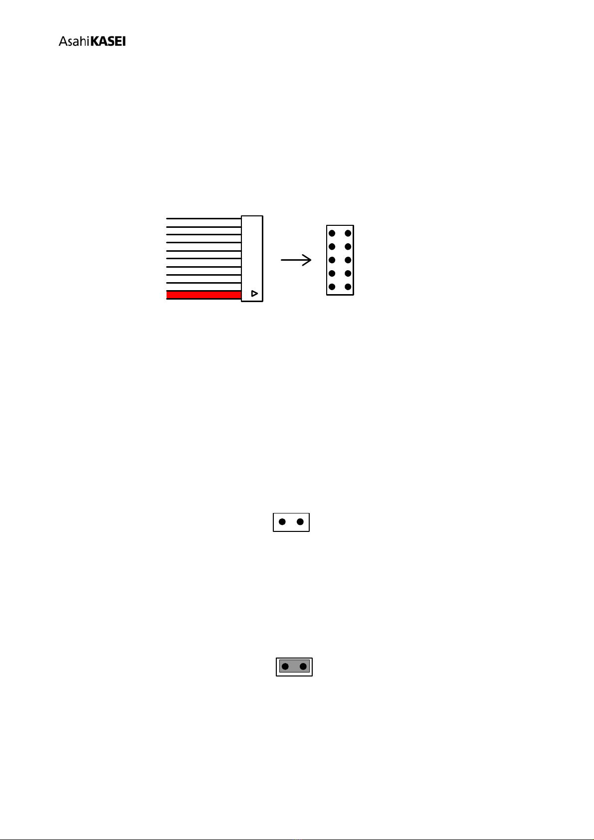
The AK4220 can be controlled via the printer port (parallel port) of IBM-AT compatible PC. Connect printer port
(parallel port) of PC and PORT2 (CTRL) of AKD4220-A by 10-wire flat cable (packed with AKD4220-A).
Take care of the direction of 10-pin connector and 10-pin header.
The control software packed with this evaluation board supports 4-wire serial control only.
Connect
CDTO/SDA
CCLK/SCL
CDTI/SDA
10-pin
header
10-pin
connector
10-wire
flat cable
PC
AKD4220-A
CSN
56
110
PORT2
CTRL
Red
Figure 2. 10-wire flat cable, 10-pin connector, and 10-pin header
(1) 4-wire Serial Control Mode
The jumper pins should be set to the following.
(2) I2C-bus Control Mode
The jumper pins should be set to the following. <Default>
JP8
I2C
JP8
I2C

[AKD4220-A]
<KM083401> 2012/04
- 6 -
Input / Output circuit & Set-up jumper pin for Input / Output circuits
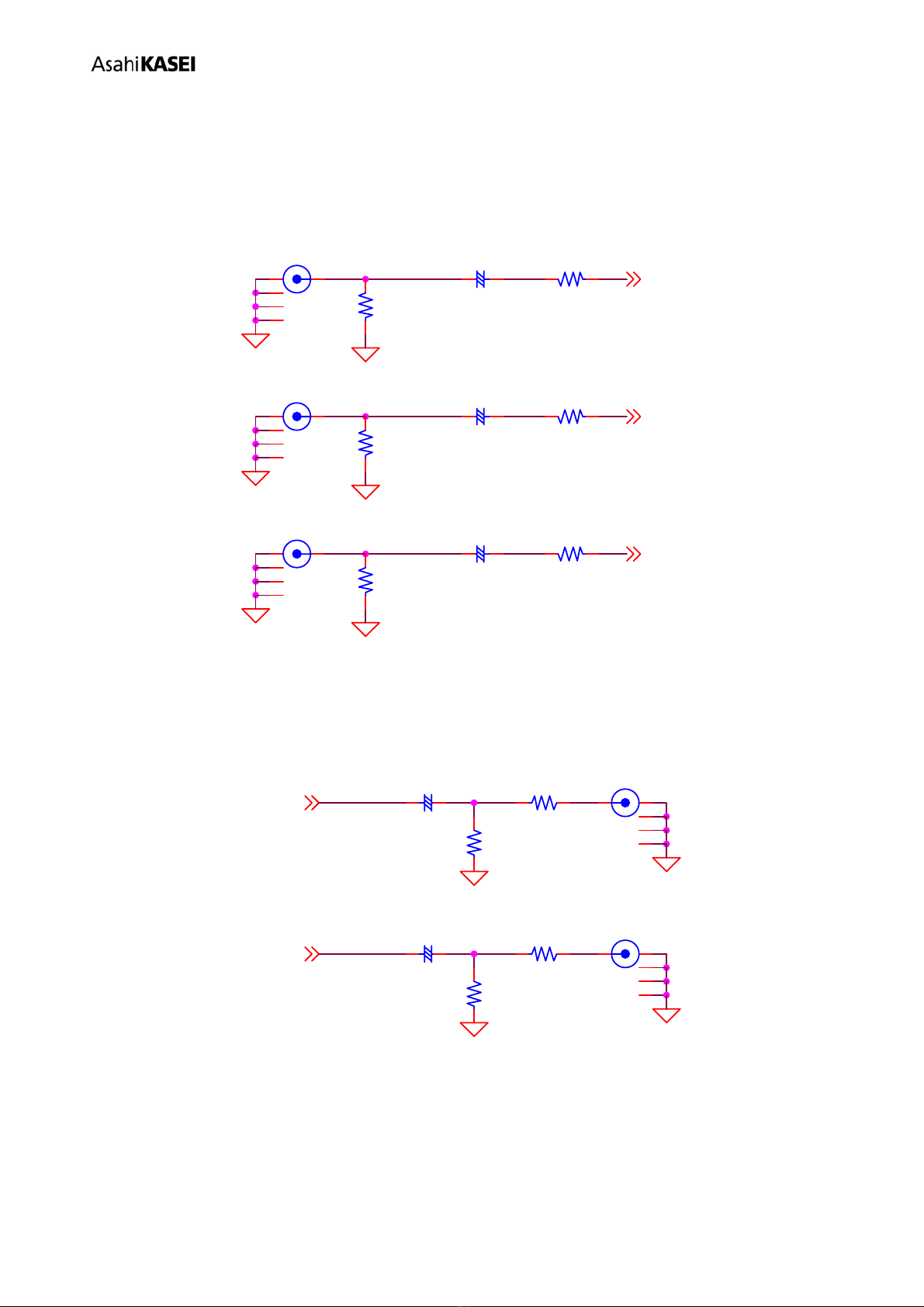
(1) Audio Input Circuit
GND1, LIN+1, RIN+1∼GND7, LIN+7, RIN+7 Input circuits
12
3
4
5
J4
LIN+1
R10
(open)
LIN+1
12
3
4
5
J7
RIN+1
R13
(open)
RIN+1
R73
(short)
R74
(short)
R75
(short)
+
C18
0.47u
12
3
4
5
J1
GND1
+
C21
0.47u
R7
(open)
+
C24
0.47u
GND1
Figure 3. GND, LIN+, RIN+ Input circuit
(2) Audio Output Circuit
LOUT1/ROUT1 ∼LOUT3/ROUT3 Output circuits
R28
300
+
C39
10u
1 2
3
4
5
J22
LOUT1
LOUT1
R29
300
+
C40
10u
1 2
3
4
5
J23
ROUT1
ROUT1
R94
22k
R95
22k
Figure 4. LOUT/ROUT Output circuit

[AKD4220-A]
<KM083401> 2012/04
- 7 -
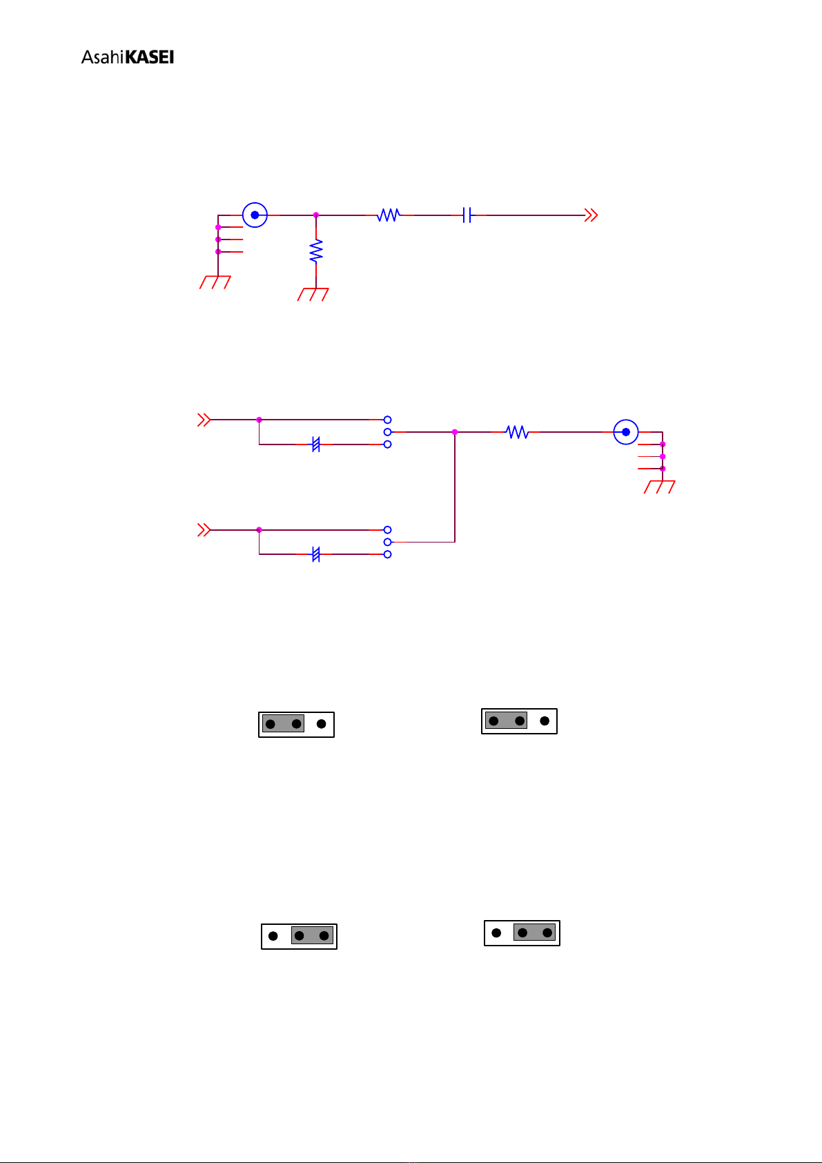
(3)Video Input Circuit
VIN1 ∼VIN6 Input circuits
C64
0.1u
R58
(short)
R61
75
VIN1
12
3
4
5
J28
VIN1
Figure 5. VIN Input circuit
(4)Video Output Circuit
VOUT1 ∼VOUT3 Output circuits
1 2
3
4
5
J34
VOUT1
VFB1
R70
75
VOUT1
+
C45
2.2u
+
C70
100u
JP2
SAG1-1
1
0
0
1
JP3
SAG1-2
Figure 6. VOUT Output circuit
(4-1) “DC Output” is output from J34, J35 and J36 connector. (SAGN bit = 1) <Default>
(4-2) “SAG Trimming Circuit ” is output from J34, J35 and J36 connector. (SAGN bit = 0)
JP2/JP4/JP6
SAG1-1/SAG2-1/SAG3-1
10
JP3/JP5/JP7
SAG1-2/SAG2-2/SAG3-2
10
JP2/JP4/JP6
SAG1-1/SAG2-1/SAG3-1
10
JP3/JP5/JP7
SAG1-2/SAG2-2/SAG3-2
10

[AKD4220-A]
<KM083401> 2012/04
- 8 -
Control Software Manual
Set-up of evaluation board and control software
1.Set up the AKD4220-A evaluation board according to the above instructions.
2.Connect PC with AKD4220-A by 10-line type flat cable (packed with AKD4220-A). Please note the direction of the
10pin header.
3.Insert the CD-ROM labeled “AKD4220-A Evaluation Kit” into the CD-ROM drive.
4.Access the CD-ROM drive and double-click “akd4220-a.exe.” Set up the control program as needed.
5.Evaluate according to the following.
Operation flow
1. Set up and open the control program as above.
The following operation screen will be shown. (Default setting)
Figure 1. Control software window
2. Click “Port Reset” button.
Enter desired register setting and begin evaluation.

[AKD4220-A]
<KM083401> 2012/04
- 9 -
Button Functions
1. [Port Reset] : Set up USB interface board (AKDUSBIF-B).
2. [Write default] : Initialize all register settings.
3. [All Write] : Write all registers currently displayed.
4. [All Read] : Read all current register settings.
5. [Save] : Save the current register setting to .akr file.
6. [Load] : Load register setting from saved .akr file.
7. [All Reg Write] : Write to all registers by keyboard operation
8. [Data R/W] : Read/write register data by keyboard operation.
9. [Sequence] : The sequence of register setting can be set and executed.
10. [Sequence (File)] : The sequence created by [Sequence] can be assigned and executed.
11. [Write] : Write data by mouse operation.
12. [Read] : Read data by mouse operation.
13. [Read] : Read and display all current register setting in register window (on right side of main window).
Different from [All Read] as it does not reflect to the register map.
Data Indication
Input data is indicated on the register map. Button DOWN with red label indicates “H” or “1” and button UP with blue
label indicates “L” or “0”. Blank buttons are not defined in the datasheet.

[AKD4220-A]
<KM083401> 2012/04
- 10 -
Explanation of each dialog
1. [Write Dialog]: Dialog to write data by mouse operation
There are dialogs corresponding to each register address.
Click the [Write] button corresponding to each register address to open the dialog. If the checkbox next to the
register is checked, “H” or “1” will be written to the register. If it is unchecked, “L” or “0” will be written to the
register.
Click [OK] button to execute the write to the registers. To cancel, click [Cancel] button.
2. [Save] and [Load]
2-1. [Save]
Save the current register setting data. The extension of file name is “akr”.
(Operation flow)
(1) Click [Save] Button.
(2) Enter a file name and push [Save] Button to save settings to .akr file.
2-2. [Load]
Write the register setting saved using [Save].
(Operation flow)
(1) Click [Load] Button.
(2) Select file (*.akr) and Click [Open] Button.
3. [All Register Write Dialog]
Write and execute the register settings created by [SAVE] function. Click [All Reg Write] button to open the dialog
shown in Figure 2.
Figure 2. [All Reg Write] window

[AKD4220-A]
<KM083401> 2012/04
- 11 -
3-1. [Open] and [Write] button
(1) Click [Open] button and select register setting file (*.akr).
(2) Click [Write] button to execute register setting.
3-2. [Save] and [Open] buttons on right side
[Save]: Save register setting file as *.ak5 file.
[Open]: Load register setting file (*.ak5).
3-3. Note
(1) All files must be in same folder for [Save] and [Open] function on right side.
(2) If register setting is changed by [Save] Button in main window, the file should be loaded again in order to reflect the
change.
4. [Data Read/Write Dialog]: Dialog to write data by keyboard operation
Address Box: Input registers address in 2 hexadecimal figures.
Data Box: Input registers data in 2 hexadecimal figures.
Mask: Input mask data in 2 hexadecimal figures. This value is AND-ed with input data.
Click [Write] button to execute the write to the registers. To cancel, click [Close] button.
To read the current register value for the specified address, click [Read].
5. [Sequence Dialog]
Set and execute register setting sequence.
(1) Click [Sequence] Button.
(2) Set the control sequence.
Enter Address, Data and Interval time. Enter “-1” to Address to end sequence at that step.
(3) Click [Start] button to execute sequence.
The sequence can be paused by entering Interval="-1". Click [START] button to restart the sequence from the paused
step.
This sequence can be saved and opened by [Save] and [Open] button at the bottom right of the dialog. The extension of
file name is “aks”.

[AKD4220-A]
<KM083401> 2012/04
- 12 -
Figure 3. [Sequence] window
6. [Sequence(File) Dialog]
Write and execute sequence created in [Sequence]. Click [Sequence(File)] button to open the dialog shown in Figure 4.
Figure 4. [Sequence(File)] window

[AKD4220-A]
<KM083401> 2012/04
- 13 -
6-1. [Open] buttons on left side and [Start] buttons
(1) Click [Open] button and select the sequence file (*.aks).
(2) Click [Start] button to execute the sequence.
6-2. [Save] and [Open] buttons on right side
[Save]: Save sequence file. The file name is *.ak4.
[Open]: Load saved sequence file (*.ak4).
6-3. Note
(1) [Sequence(File)] does not support the pause function of [Sequence] function.
(2) All files must be in same folder for [Save] and [Open] function.
(3) When the sequence is changed in [Sequence], the file should be loaded again in order to reflect the changes.
7. [Loop Dialog]: Dialog to evaluate ATT of VOL Control
Under the Tool tab in the main window, there is a button for [Loop Setting].
Address Box: Input registers address in 2 hexadecimal figures.
Start Data Box: Input start data in 2 hexadecimal figures.
End Data Box: Input end data in 2 hexadecimal figures.
Interval Box: Interval for data write..
Step Box: Data changes by this step.
Mode Select Box:
By checking this check box, the data will countdown to start data after reaching end data.
[Example] Start Data = 00, End Data = 09
Data flow: 00 01 02 03 04 05 06 07 08 09 09 08 07 06 05 04 03 02 01 00
If unchecked, the loop ends after data reaches end data.
[Example] Start Data = 00, End Data = 09
Data flow: 00 01 02 03 04 05 06 07 08 09
To write input data to AK4220, click [OK] button. To cancel, click [Cancel] button.

[AKD4220-A]
<KM083401> 2012/04
- 14 -
MEASUREMENT RESULTS
Audio
[Measurement condition]
•Measurement unit : Audio Precision System two Cascade
•BW :10Hz∼20kHz
•Power Supply : AVDD=5V, VVDD1=5V, VVDD2=5V, DVDD=3V
•Temperature : Room
•Measurement signal line path: LIN+1/RIN+1 →LOUT/ROUT
Parameter Input signal Measurement filter Results [dB]
S/(N+D) at 1Vrms Output 1kHz, 0dBV 20kLPF 93.2 / 93.1
DR 1kHz, -60dBV 22kLPF, A-weighted 96.2 / 96.2
S/N Off 22kLPF, A-weighted 96.2 / 96.1
Plots
Figure 1-1. FFT (1kHz, 0dBV input) at 1Vrms output
Figure 1-2. FFT (1kHz, -60dBV input)
Figure 1-3. FFT (Noise floor)
Figure 1-4. THD+N vs. Input Level (fin=1kHz)
Figure 1-5. THD+N vs. fin (Input Level=0dBFS)
Figure 1-6. Linearity (fin=1kHz)
Figure 1-7. Frequency Response (Input Level=0dBV)
Figure 1-8. Crosstalk (Input Level=0dBV)

[AKD4220-A]
<KM083401> 2012/04
- 15 -
Video
[Measurement condition]
•Signal Generator : Sony Tectonics TG2000
•Measurement unit : Sony Tectonics VM700T
•Power Supply : AVDD=5V, VVDD1=5V, VVDD2=5V, DVDD=3V
•Temperature : Room
•Measurement signal line path: VIN1 →VOUT1
Parameter Measurement conditions Results Unit
S/N Input = 0% flat field
Filter = Uni-weighted,
BW= 15kHz to 5MHz
SAG = 1
72.4 dB
Crosstalk Input = 100%red(ENCRC),
Measured at VOUT -74.0 dB
DG Input = Modulated Lamp
SAG = 1 0.22 %
DP Input = Modulated Lamp
SAG = 1 0.91 deg.
Plots
Figure 2-1. Noise spectrum (Input=0%flat field, BW=15kHz to 5MHz, uni weighted, SAG=1)
Figure 2-2. Frequency Response (Input= Multi Burst, SAG=1)
Figure 2-3 Crosstalk (Input= 100% red (VIN1), measured at VOUT1)
Figure 2-4 Crosstalk (Input= 100% red (VIN2), measured at VOUT1)
Figure 2-5 DG, DP (Input= Modulated Lamp, SAG=1)

[AKD4220-A]
<KM083401> 2012/04
- 16 -
Plots (Audio)
A
KM 11/17/05 10:47:28AK4220 FFT LIN1/RIN1-->LOUT1/ROUT1 input=0dBV
-160
+0
-150
-140
-130
-120
-110
-100
-90
-80
-70
-60
-50
-40
-30
-20
-10
d
B
V
20 20k50 100 200 500 1k 2k 5k 10k
Hz
Figure1-1. FFT (fin=1kHz Input Level=0dBV)
A
KM 11/17/05 10:55:52AK4220 FFT LIN1/RIN1-->LOUT1/ROUT1 input=-60dBV
-160
+0
-150
-140
-130
-120
-110
-100
-90
-80
-70
-60
-50
-40
-30
-20
-10
d
B
V
20 20k50 100 200 500 1k 2k 5k 10k
Hz
Figure-1-2. FFT (fin=1kHz Input Level=-60dBV)

[AKD4220-A]
<KM083401> 2012/04
- 17 -
A
KM 11/17/05 11:18:13AK4220 FFT LIN1/RIN1-->LOUT1/ROUT1 Input=no signal
-160
+0
-150
-140
-130
-120
-110
-100
-90
-80
-70
-60
-50
-40
-30
-20
-10
d
B
V
20 20k50 100 200 500 1k 2k 5k 10k
Hz
Figure1-3. FFT (Noise Floor)
A
KM 11/17/05 11:05:06AK4220 LIN1/RIN1-->LOUT1/ROUT1 THD vs.Input Level
fin=1kHz
-100
-70
-98
-96
-94
-92
-90
-88
-86
-84
-82
-80
-78
-76
-74
-72
d
B
r
A
-120 +0-110 -100 -90 -80 -70 -60 -50 -40 -30 -20 -10
dBV
Figure1-4. THD+N vs. Input level (fin=1kHz)

[AKD4220-A]
<KM083401> 2012/04
- 18 -
A
KM 11/17/05 11:13:51AK4220 LIN1/RIN1-->LOUT1/ROUT1 THD vs.Input Frequency
Input=0dB
-100
-70
-98
-96
-94
-92
-90
-88
-86
-84
-82
-80
-78
-76
-74
-72
d
B
r
A
20 20k50 100 200 500 1k 2k 5k 10k
Hz
Figure1-5. THD+N vs. Input Frequency (Input level=0dBV)
A
KM 11/17/05 11:22:34AK4220 LIN1/RIN1-->LOUT1/ROUT1 Linearityfin=1kHz
-120 +0-110 -100 -90 -80 -70 -60 -50 -40 -30 -20 -10
dBV
-120
+0
-110
-100
-90
-80
-70
-60
-50
-40
-30
-20
-10
d
B
r
A
Figure1-6.Linearity (fin=1kHz)

[AKD4220-A]
<KM083401> 2012/04
- 19 -
A
KM 05/18/06 13:15:12AK4220 LIN+1/RIN+1-->LINEOUT FrequencyResponse Input=0dBV
last.at2
-1
+1
-0.9
-0.8
-0.7
-0.6
-0.5
-0.4
-0.3
-0.2
-0.1
+0
+0.1
+0.2
+0.3
+0.4
+0.5
+0.6
+0.7
+0.8
+0.9
d
B
r
A
2k 20k4k 6k 8k 10k 12k 14k 16k 18k
Hz
Figure1-7. Frequency Response (Input level=0dBV)
Figure1-8. Crosstalk (Input level=0dBV)

[AKD4220-A]
<KM083401> 2012/04
- 20 -
Plots(Video)
Figure 2-1. Noise spectrum (Input=0%flat field, BW=15kHz to 5MHz, uni weighted, SAG=1)
Figure 2-2. Frequency Response (Input= Multi Burst, SAG=1)
Table of contents
Other Asahi KASEI Motherboard manuals

Asahi KASEI
Asahi KASEI AKM AKD5538-B User manual

Asahi KASEI
Asahi KASEI AKD4709-A User manual

Asahi KASEI
Asahi KASEI AKD4382A-SB User manual

Asahi KASEI
Asahi KASEI AKD4140-B User manual

Asahi KASEI
Asahi KASEI AK5704 User manual

Asahi KASEI
Asahi KASEI AK9720 Installation instructions

Asahi KASEI
Asahi KASEI AKD2300 User manual

Asahi KASEI
Asahi KASEI AKD5538-B User manual