Asahi KASEI AKD2300 User manual

[AKD2300]
<KM103501> 2015/02
1
Board Function
The AKD2300 is the evaluation board for the AK2300.The AKD2300 has on-board(internal) clock generate function.
The evaluation can begin by setting the DIP Switches. External resistance and capacitors of the I/O amplifier can be
changed. It provides easy the setting of the parameter of the desire.
Board Layout
The AKD2300 has six following components.
1 : Power supply pins
2 : The PLD setting Switches
3 : The AK2300 setting Switches
4 : Digital Interface
5 : Analog Interface
6 : Path selection Jumpers of the AK2300 input data
4.Degital Interface
3.The AK2300 setting Switches
2.The PLD setting Switches
6. Path selection Jumpers
5.Analog Interface
1.Power supply pins
AKD2300
AK2300 Evaluation Board

[AKD2300]
<KM103501> 2015/02
2
Power supply pins
Power supply pins is VDD,VSS,LVDD,LVDDX,VDDX_3.3V,VSSX.
Please feed 1.7V~3.6V to the LVDD and LVDDX, and feed 2.6V~3.6V to the VDD. Supply 3.3V to VDDX_3.3V.
However, set to become VDD≧LVDD. Connect VSS and VSSX with GND.
Each power supply and GND can be connected by the JP1 and the JP2 and the JP3 and the JP4.
These jumpers settings are shown below. When the digital noise influences on analog characteristics, please remove
these jumpers to separate these power line.
Jumper Name
Function
JP1
LVDD and LVDDX are connected.
JP2
VDD and VDDX_3.3V are connected.
JP3
VDD and LVDD are connected.
JP4
VSS and VSSX are connected.
The PLD Setting Switches
The DSW2 and the DSW3 and the DSW4 are switches of the PLD settings. (DSW1 is unused)
The functions of the switches are shown below.
DSW2
Switch Name
Function
FRQ2
FRQ1
FRQ0
BCLK Selection
This switch is selects internal BCLK frequency.
FRQ2
FRQ1
FRQ0
Frequency
0
0
0
64kHz
0
0
1
128kHz
0
1
0
256kHz
0
1
1
512kHz
1
0
0
1024kHz
1
0
1
2048kH
1
1
*
Don’t care

[AKD2300]
<KM103501> 2015/02
3
DSW3
Switch Name
Function
SYNC1
SYNC0
Frame sync signal selection (Available in INT mode only)
Output a sync signal for external measurement systems to the TP8(RSYNC) and the
TP9(TSYNC).
SYNC1
SYNC0
Output Signal
0
0
Refer to the Figure 1.
0
1
Refer to the Figure 1.
1
0
Refer to the Figure 1.
1
1
Refer to the Figure 1.
EXT/INT
Set the method of supplying BCLK and FS.
EXT:The external clock feed from digital interface.
INT:On-board(internal) clock used.
BCLK
FS
<Short Frame>
SYNC[1:0]
00
01
10
11
BCLK
FS
<Long Frame>
SYNC[1:0]
00
01
10
11
Figure 1

[AKD2300]
<KM103501> 2015/02
4
DSW4
Switch Name
Function
PCM1
PCM0
PCM Interface setting1
This switch selects data format of PCM interface.
PCM1
PCM0
PCM Interface
0
0
A-Law (DIF0 = L)
0
1
μ-Law (DIF0 = H)
1
*
Linear (DIF0 = FS)
SF/LF
PCM Interface setting2
This switch selects FS type at the INT mode.
SF:Short Frame(Refer to the Figure 1)
LF:Long Frame(Refer to the Figure 1)
The AK2300 Setting Switches
The SW1 and the SW2 and the DSW4-4 are switches of the AK2300 settings.
The functions of the switches are shown below.
SW1
Switch Name
Function
MUTEN
PCM Codec output settings
This switch sets the output of PCM CODEC mute.
OFF:Normal operation
ON:Mute
SW2
Switch Name
Function
PDN
Power down mode settings
This switch sets power-down mode of the AK2300.
OFF:Normal operation
ON:Power down mode

[AKD2300]
<KM103501> 2015/02
5
BCLK
FS
DX MSB
DR Don't
care
LSB
MSB LSB
<JST>
BCLK
FS
DX MSB
DR Don't care
LSB
MSB LSB
<DLY>
DSW4-4
Switch Name
Function
DLY/JST
PCM Interface settings3
This switch selects input and output timing of PCM data.
DLY(DIF1 = L):MSB of DX/DR are input/output by next rising edge of BCLK after the
rising edge of FS. (Refer to the Figure 2)
JST(DIF1 = H):MSB of DX/DR are input/output by rising edge of FS. (Refer to the
Figure 2)
Figure 2

[AKD2300]
<KM103501> 2015/02
6
-
+
SP3
GST
VFTN
SP2
SP5SP4
VFTN
VR
SP1
VR
Digital Interface
The AKD2300 has CN1 as a digital interface.
Pin No
Signal
Name
Function
1
DX
This pin outputs the DX data from the AK2300.
3
DR
This pin inputs the DR data to the AK2300.
When the JP5 is used, As for DX data the loop backing is by DR data.
5
BCLK
This pin inputs external signal BCLK. *
7
FS
This pin inputs external signal FS. *
9
DIF0
This pin inputs external signal DIF0. *
11
DIF1
This pin inputs external signal DIF1.
13
MUTEN
This pin inputs external signal MUTEN.
15
PDN
This pin inputs external signal PDN.
16
VDD
This pin is connected with VDD.
2/4/6/8
10/12/14
VSS
These pins are connected with VSS.
*:Available in EXT mode only.
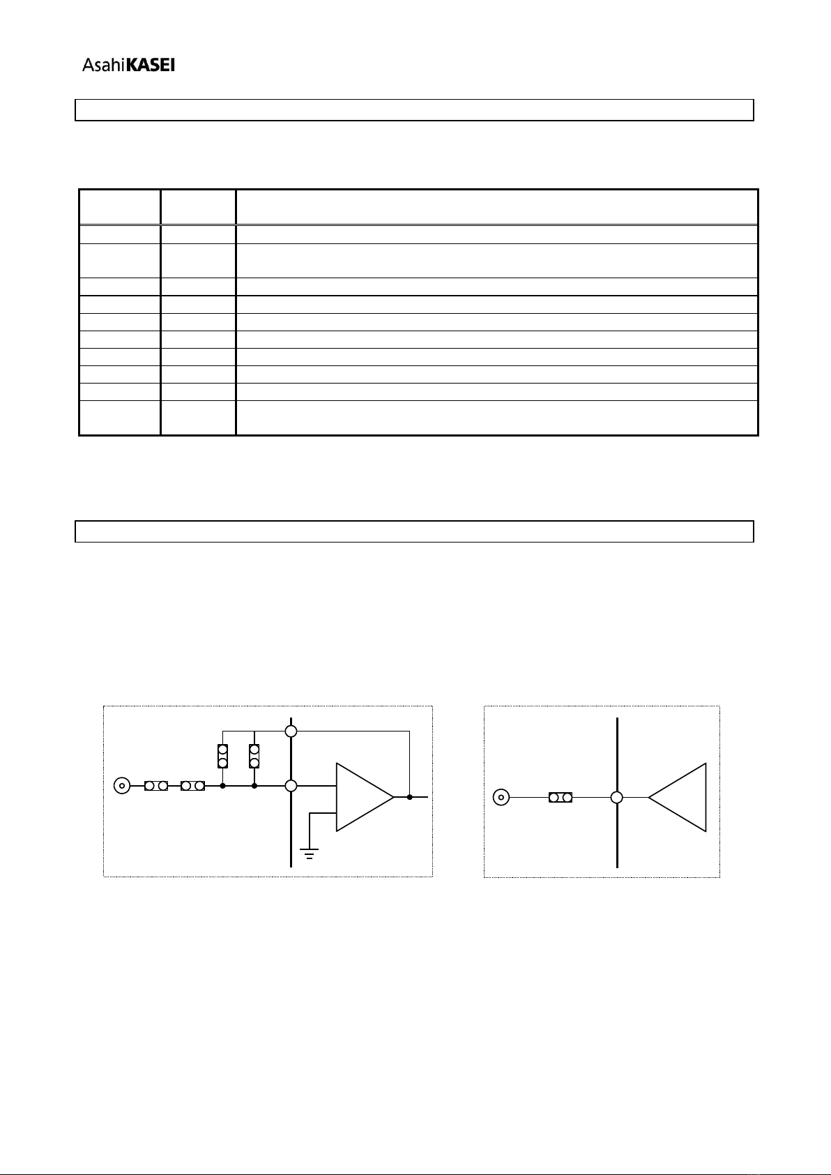
Analog Interface
The AKD2300 has BNC connector VFTN for transmission amplifier input and BNC connector VR for reception
amplifier output.
Insert resistance and capacitors of each amplifier in the socket pin. It provides easy the setting of the parameter of the
desire. When shipped, it is set in the parameter of the application circuit of the AK2300 data sheets.
◆Analog input circuit ◆Analog output circuit
Figure 3

[AKD2300]
<KM103501> 2015/02
7
Path selection jumpers of the AK2300 input data
The JP6 and the JP7 and the JP8 are selected input signal (MUTEN,PDN,DIF1) path of the AK2300.
These jumpers settings are shown below.
Jumper Name
State
Function
JP6
Short
The MUTEN pin inputs the SW1 setting.
Open
The MUTEN pin inputs the CN1 setting.
JP7
Short
The PDN pin inputs the SW2 setting.
Open
The PDN pin inputs the CN1 setting.
JP8
Short
The DIF1 pin inputs the DSW4(DLY-JST) setting.
Open
The DIF1 pin inputs the CN1 setting.
Connection selection jumpers of the AK2300 Exposed Pad
Jumper Name
State
Function
JP9
Short
Exposed Pad of the AK2300 and VSS are connected.
Open
Exposed Pad of the AK2300 is Opened.

[AKD2300]
<KM103501> 2015/02
8
VSS
VSS
2
1
C9
0.056uF(+-30%)
10k
BNC1
VR
1
2
DX
JP2
1 2
GST
HEADER PIN16
13 2
15 4
11 6
1 8
910
712
514
316
6
JP9
1 2
SYNC1
1
SP2
CN1
TP2
2
1
VSS
2
C7
0.1uF
C4
1uF
LVDDX
7
VREF
2 1
C10
0.1uF
I_DR
DLY_JST
SP5
LVDD
1
TP10
I_FS
VSS
2
VSSX
2
1
2
FRQ_SEL2
C2
10uF
LVDD
1
VDDX_3.3V
DSW1
SYNC0
3
1
FRQ_SEL1
SP4
JP4
1 2
I_PDN
1
RSV1
SO1
QN1-016050-202
8
7
6
5
4
3
2
116
15
14
13
9
10
11
12
EXPAD
2
2
VSS
C1
10uF
JP5
1 2
VDD
INT_EXT
TP1
4
FRQ_SEL0
Y1 4.096MHz
U4B
TC4069UBF
3 4
147
1
R4
1M
U4A
1 2
BNC2
VFTN 1
2
VSSX
C15
22pF
3
RD2
2
C16
22pF
CLK
VDDX_3.3V
C17
0.1uF
TP7
TP8
TP4
TP9
TP6
TP5
DLY_JST
C3
10uF
1
2
2
PCM1
TSYNC
EXPAD
I_DIF1
1
JP3
1 2
DR
JP1
1 2
2
R1
10k
PLLC
4
VSS
DX
LVDD
DIF0
FS
BCLK
DR
VDDX_3.3V
2
RD1
2
PCM0
2
C11
0.1uF
RSV2
LVDD
O_DX
I_MUTEN
2
TP12
2
TP11
1
SP1
I_BCLK
PDN
RSV0
VDD
VR
DIF1
GST
VFTN
LF_SF
MUTEN
VREF
TP3
2
XC9572XL-VQ44
U2
VCCIO 26
VCC 35
VCC 15
I/O
14
I/O
18
I/O
19
I/O
20
I/O
21
I/O
22
I/O
8
I/O
12
I/O
13
TCK 11
GND 4
GND 17
GND 25
I/O
5
I/O 2
I/O 42
I/O 32
I/O 31
TDO 24
TDI 9
TMS 10
I/O 29
I/O 28
I/O 23
I/O 27
I/O 39
I/O 40
I/O 41
I/O/GCK1
43
I/O/GCK2
44
I/O/GCK3 1
I/O/GSR
33 I/O/GTS1
36 I/O/GTS2
34
I/O
6
I/O
7I/O 30
I/O 37
I/O 38
I/O 16
I/O 3
JP8
1 2
C18
0.1uF
TP13
1
1
2
RSYNC
U1
AK2300
LVDD
12
VDD
3
VSS
10
GST
6
VFTN
7
DR
16
BCLK
15
FS
14
DIF0
13
DX
11
DIF1
5
VR 4
PLLC 9
VREF 8
MUTEN
1
PDN
2
EXPAD
2
I_FS
1
VSSX
DSW4
PCM I/F
1
5
C8
0.1uF 1
VDDX_3.3V
T1
1
I_DIF0
2
VSS
I_BCLK
SP3
MUTEN
6
T2
I_DIF0
C19
0.1uF
EXPAD
VSS
C5
1uF
2
U3
TC74VCX244FT
A1
2
A2
4A3
6A4
8
1OE
1
Y1 18
Y2 16
Y3 14
Y4 12
VCC 20
GND 10
A5 11
A6
13
A7
15
A8
17 Y5
9
Y6 7
Y7 5
Y8 3
2OE
19
VDD
VFTN
3
MONI3
HEADER PIN6
1
2
3
4
5 6
C6
10uF
VSS
2
T3
MONI2
1
VSS
2
T4
VDDX_3.3V
PDN
C12
0.1uF
MONI0
1
6
5
4
BCLK
MONI1
1
VSSX
VDDX_3.3V
1
2
3
6
5
4
LVDDX
1
1
2
3
T5
6
5
4
VSSX
VDD
1
VDD
DSW2
FRQ_SEL
1
2
3
8
7
6
7
4
FS
VSS
CN2
5
PLLC
1
VR
2
DSW3
1
LVDDX
5
JP7 12
DIF1
R2
10k R3
10k
11
SW1
1 2
1C13
0.1uF
1C14
0.1uF
1
2 2
JP6 12 22
VSSX
VSS
SW2
1 2
VSS
1
2
DIF0
2
VDD VSS
VSS
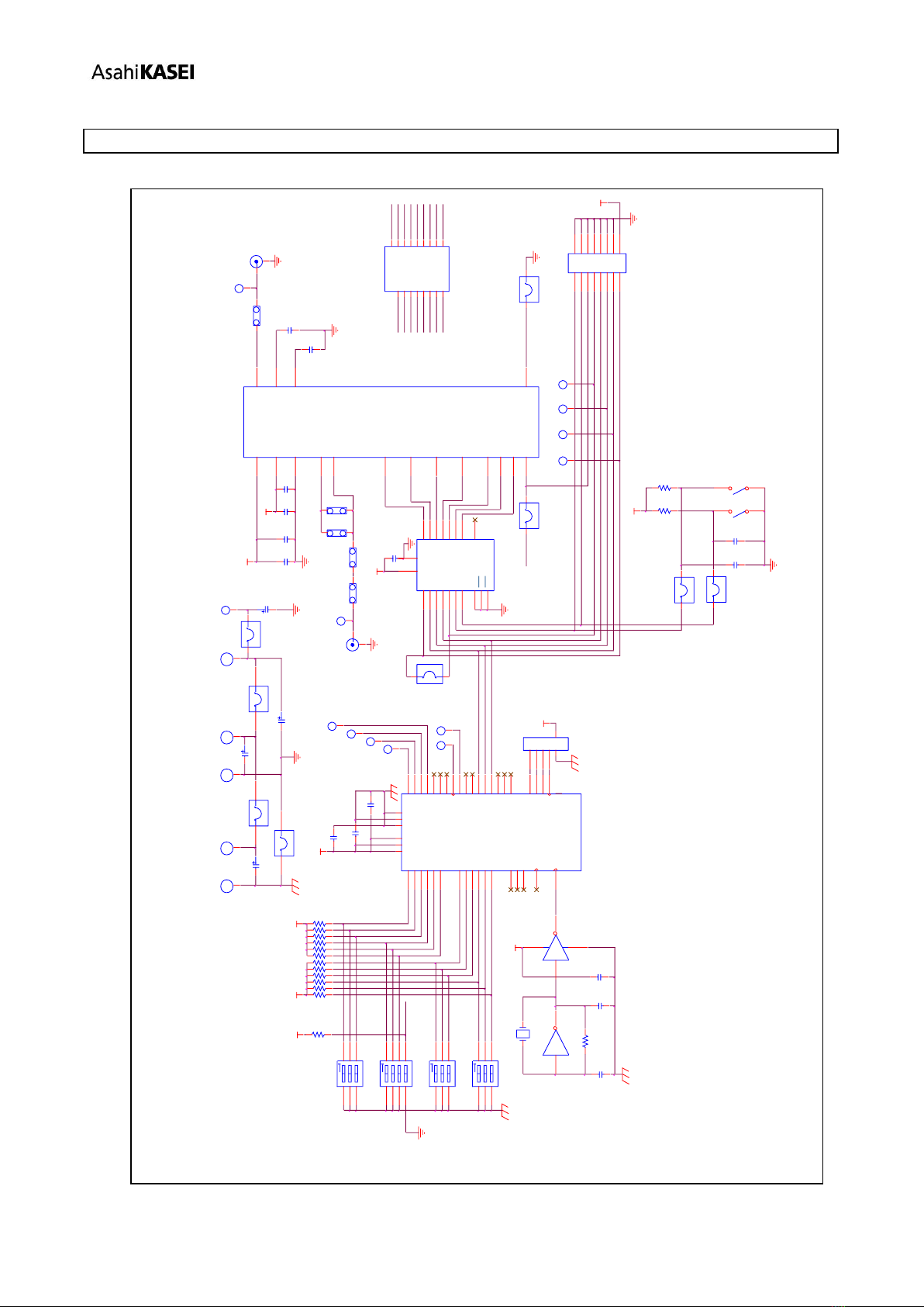
Board Circuit
The circuit chart of the AKD2300 is shown in the following.

[AKD2300]
<KM103501> 2015/02
9
Revision History
Date
(yy/mm/dd)
Manual
Revision
Board
Revision
Reason
Page
Contents
10/05/13
KM103500
0
First edition
-
15/02/23
KM103501
0
Add
9-10
“Revision History” and “IMPORTANT NOTICE” are
added.

[AKD2300]
<KM103501> 2015/02
10
IMPORTANT NOTICE
0. Asahi Kasei Microdevices Corporation (“AKM”) reserves the right to make changes to the information
contained in this document without notice. When you consider any use or application of AKM product
stipulated in this document (“Product”), please make inquiries the sales office of AKM or authorized
distributors as to current status of the Products.
1. All information included in this document are provided only to illustrate the operation and application
examples of AKM Products. AKM neither makes warranties or representations with respect to the
accuracy or completeness of the information contained in this document nor grants any license to any
intellectual property rights or any other rights of AKM or any third party with respect to the information
in this document. You are fully responsible for use of such information contained in this document in
your product design or applications. AKM ASSUMES NO LIABILITY FOR ANY LOSSES
INCURRED BY YOU OR THIRD PARTIES ARISING FROM THE USE OF SUCH INFORMATION
IN YOUR PRODUCT DESIGN OR APPLICATIONS.
2. The Product is neither intended nor warranted for use in equipment or systems that require
extraordinarily high levels of quality and/or reliability and/or a malfunction or failure of which may cause
loss of human life, bodily injury, serious property damage or serious public impact, including but not
limited to, equipment used in nuclear facilities, equipment used in the aerospace industry, medical
equipment, equipment used for automobiles, trains, ships and other transportation, traffic signaling
equipment, equipment used to control combustions or explosions, safety devices, elevators and escalators,
devices related to electric power, and equipment used in finance-related fields. Do not use Product for
the above use unless specifically agreed by AKM in writing.
3. Though AKM works continually to improve the Product’s quality and reliability, you are responsible for
complying with safety standards and for providing adequate designs and safeguards for your hardware,
software and systems which minimize risk and avoid situations in which a malfunction or failure of the
Product could cause loss of human life, bodily injury or damage to property, including data loss or
corruption.
4. Do not use or otherwise make available the Product or related technology or any information contained
in this document for any military purposes, including without limitation, for the design, development, use,
stockpiling or manufacturing of nuclear, chemical, or biological weapons or missile technology products
(mass destruction weapons). When exporting the Products or related technology or any information
contained in this document, you should comply with the applicable export control laws and regulations
and follow the procedures required by such laws and regulations. The Products and related technology
may not be used for or incorporated into any products or systems whose manufacture, use, or sale is
prohibited under any applicable domestic or foreign laws or regulations.
5. Please contact AKM sales representative for details as to environmental matters such as the RoHS
compatibility of the Product. Please use the Product in compliance with all applicable laws and
regulations that regulate the inclusion or use of controlled substances, including without limitation, the
EU RoHS Directive. AKM assumes no liability for damages or losses occurring as a result of
noncompliance with applicable laws and regulations.
6. Resale of the Product with provisions different from the statement and/or technical features set forth in
this document shall immediately void any warranty granted by AKM for the Product and shall not create
or extend in any manner whatsoever, any liability of AKM.
7. This document may not be reproduced or duplicated, in any form, in whole or in part, without prior
written consent of AKM.
Table of contents
Other Asahi KASEI Motherboard manuals

Asahi KASEI
Asahi KASEI AKD4709-A User manual

Asahi KASEI
Asahi KASEI AKD4140-B User manual

Asahi KASEI
Asahi KASEI AKD5538-B User manual

Asahi KASEI
Asahi KASEI AKM AKD5538-B User manual

Asahi KASEI
Asahi KASEI AKD4220-A User manual

Asahi KASEI
Asahi KASEI AK9720 Installation instructions

Asahi KASEI
Asahi KASEI AK5704 User manual

Asahi KASEI
Asahi KASEI AKD4382A-SB User manual