ASAHI AKD4671-B User manual

[AKD4671-B]
<KM089001> 2008 / 03
- 1 -
GENERAL DESCRIPTION
AKD4671 is an evaluation board for the AK4671, stereo CODEC with built-in Microphone-Amplifier,
Receiver-Amplifier and Headphone-Amplifier.
The AKD4671 can evaluate A/D converter and D/A converter separately in addition to loopback mode
(A/D →D/A). The AKD4671-B also has the digital audio interface and can achieve the interface with
digital audio systems via opt-connector.
Ordering guide
AKD4671 --- Evaluation board for AK4671
(Cable for connecting with printer port of IBM-AT,compatible PC and control
software are packed with this. This control software does not support Windows NT.)
FUNCTION
•DIT/DIR with optical input/output
•10pin Header for Digital Audio I/F, PCM I/F (Baseband, Bluetooth)
•BNC connector for an external clock input
•10pin Header for serial control mode
Control I/F
10Pin Header
REG
AK4114
DIR
DIT
Opt In
AK4671
AVDDSAVDD
LIN2/3/4
RIN2/3/4
DVDD
LIN1/RIN1
Digital Audio I/F
10Pin Header
GND
REG
3.3 V
ROUT1/2/3
LOUT1/2/3
Opt Out
Baseband I/F
10Pin Header
Bluetooth I/F
10Pin Header
TVDD2
TVDD3
SAIN1/2/3
SAIN3
MIC
Jack
Control I/F
SAR ADC
10Pin Header
VSS1 VSS2 VSS3 VSS4
TX
RX
HP
Jack
PVDD
Figure 1. AKD4671-B Block Diagram
* Circuit diagram and PCB layout are attached at the end of this manual
AK4671 Evaluation board Rev.1
AKD4671
-
B

[AKD4671-B]
<KM089001> 2008 / 03
- 2 -
Board Outline Chart
Outline Chart
D3V DGND VCC1 TVDD3 TVDD2 DVDD AGND REGAVDDSAVDDPVDD SAIN1 SAIN3
LIN1/RIN1
LIN
RIN
LOUT
ROUT
HP
U1
AK4114
CTRL
Bluetooth
Baseband
DSP
EXT
EXT1
X1
X2
U7
TX
RX
DIPSW
JP30
(GND)
1
10
1
10
1
10
1
10
PORT1
PORT2
J12
J13
PORT4
PORT3
PORT6
PORT5
J3
J4
J1
J11
J9
J7
J5
J2
CTRL1
10
PORT7
VCC2
270mm
200mm
Figure 2. AKD4671-B Outline Chart
Comment
(1) J2, J3 (MINI-JACK)
J2 : It is analog signal input Jack. The signal is input to LIN1 / RIN1 pins.
J3 : It is analog signal output Jack. The signal is output from LOUT2 / ROUT2 pins, and JP17, JP19 should be
“short”.
(2) J1, J4, J5, J7, J9, J11 (BNC-Connector)
J1 : It is analog signal output Jack. The signal is output from LOUT pin.
J4 : It is analog signal output Jack. The signal is output from ROUT pin.
J5 : It is analog signal input Jack. The signal is input to LIN2 or LIN3 or LIN4 pins, and JP23 should be selected.
J7 : It is analog signal input Jack. The signal is input to RIN2 or RIN3 or RIN4 pins, and JP25 should be selected.
J9 : It is analog signal input Jack. The signal is input to SAIN1 or SAIN2 or SAIN3 pins, and JP28 should be selected.
J11: It is analog signal input Jack. The signal is input to SAIN3 pin.
(3) REG, AVDD, SAVDD, PVDD, DVDD, TVDD2, TVDD3, VCC1, VCC2, D3V, AGND, DGND
These are power supply connectors. Connect power supply with these pins.
As for the detail comments, refer to the setup of power supply in P4 ∼5.
(4) J12, J13 (BNC-Connector)
J12 : MCLK can be supplied from external clock for Audio I/F, and BCLK, LRCK can be generated from MCLK.
J13 : MCLK can be supplied from external clock for PCM I/F, and BCLK, LRCK can be generated from MCLK.
(5) PORT5, PORT7 (10 pin header)
PORT5 : Control port. Connect the bundled cable into this port.
PORT7 : Control port of SAR ADC.

[AKD4671-B]
<KM089001> 2008 / 03
- 3 -
(6) PORT3, PORT4, PORT 6 (10 pin header)
PORT3 : The clock and data of Baseband mode can be inputted and outputted with this connector.
PORT4 : The clock and data of DSP can be inputted and outputted with this connector.
PORT6 : The clock and data of Bluetooth mode can be inputted and outputted with this connector.
(7) PORT1, PORT2 (Optical Connecter)
PORT1 (Input): Optical digital signal (SPDIF, Fs: 32〜48kHz) is input to the AK4114.
PORT2 (Output): Optical digital signal (SPDIF, Fs: 32〜48kHz) is output from the AK4114.
[AKD4671-B]
<KM089001> 2008 / 03
- 4 -
Evaluation Board Manual
Operation sequence
1) Set up the power supply lines.
(1-1) In case of using the regulator.
Set up the jumper pins.
JP20 JP22 JP24 JP26 JP27 JP29 JP31 JP7
JP AVDD
SEL
SAVDD
SEL
PVDD
SEL
DVDD
SEL
TVDD2
SEL
TVDD3
SEL
VCC
SEL
VCC2
SEL
State Short Short Short Short Short Short Short Short
Set up the power supply lines.
Name Color Voltage Using Note Default
REG Red +5V Regulator Default: should be
connected +5V
AVDD Orange 2.2 ∼3.6V AVDD for AK4671 Default: open
typ.3.3V
open
3.3V supplied
SAVDD Orange 2.2 ∼3.6V SVDD for AK4671 Default: open
typ.3.3V
open
3.3V supplied
PVDD Orange 2.2 ∼3.6V PVDD for AK4671 Default: open
typ.3.3V
open
3.3V supplied
DVDD Orange 1.6 ∼3.6V DVDD for AK4671 Default: open
typ.3.3V
open
3.3V supplied
TVDD2 Orange 1.6 ∼3.6V TVDD2 for AK4671 Default: open
typ.3.3V
open
3.3V supplied
TVDD3 Orange 1.6 ∼3.6V TVDD3 for AK4671 Default: open
typ.3.3V
open
3.3V supplied
VCC Orange
1.6 ∼3.6V for logic Default: open
typ.3.3V
open
3.3V supplied
VCC2 Orange 1.6 ∼3.6V for logic (The voltage same
as TVDD2 and TVDD3)
Default: open
typ.3.3V
open
3.3V supplied
D3V Orange
2.7 ∼3.6V for AK4114 and logic
Default: should be
connected.
typ.3.3V
3.3V
AGND Black 0V for analog ground Default: should be
connected 0V
DGND Black 0V for logic ground Default: should be
connected 0V
Table 1. Set up the power supply lines.
(In case of using the regulator.)

[AKD4671-B]
<KM089001> 2008 / 03
- 5 -
(1-2) In case of using the power supply connectors.
Set up the jumper pins.
JP20 JP22 JP24 JP26 JP27 JP29 JP31 JP7
JP AVDD
SEL
SAVDD
SEL
PVDD
SEL
DVDD
SEL
TVDD2
SEL
TVDD3
SEL
VCC
SEL
VCC2
SEL
State Open Open Open Open Open Open Open Open
Set up the power supply lines.
Name Color Voltage Using Note Default
REG Red +5V Regulator Default: open Open
AVDD Orange 2.2 ∼3.6V AVDD for AK4671
Default: should be
connected
typ.3.3V
3.3V
SAVDD Orange 2.2 ∼3.6V SVDD for AK4671
Default: should be
connected
typ.3.3V
3.3V
PVDD Orange 2.2 ∼3.6V PVDD for AK4671
Default: should be
connected
typ.3.3V
3.3V
DVDD Orange 1.6 ∼3.6V DVDD for AK4671
Default: should be
connected
typ.3.3V
3.3V
TVDD2 Orange 1.6 ∼3.6V TVDD2 for AK4671
Default: should be
connected
typ.3.3V
3.3V
TVDD3 Orange 1.6 ∼3.6V TVDD3 for AK4671
Default: should be
connected
typ.3.3V
3.3V
VCC Orange
1.6 ∼3.6V for logic
Default: should be
connected
typ.3.3V
3.3V
VCC2 Orange 1.6 ∼3.6V for logic (The voltage same
as TVDD2 and TVDD3)
Default: should be
connected
typ.3.3V
3.3V
D3V Orange
2.7 ∼3.6V for AK4114 and logic
Default: should be
connected.
typ.3.3V
3.3V
AGND Black 0V for analog ground Default: should be
connected 0V
DGND Black 0V for logic ground Default: should be
connected 0V
Table 2. Set up the power supply lines.
(In case of using the power supply connectors.)
* Each supply line should be distributed from the power supply unit.
2) Set up the evaluation mode, jumper pins and DIP switches. (See the followings.)
3) Power on.
The AK4671 and AK4114 should be reset once bringing SW1 (DIR) and SW2 (PDN) “L” upon power-up.

[AKD4671-B]
<KM089001> 2008 / 03
- 6 -
Evaluation mode
1. Audio I/F evaluation mode
In case of AK4671 evaluation using AK4114, it is necessary to correspond to audio interface format for
AK4671 and AK4114. About AK4671’s audio interface format, refer to datasheet of AK4671. About
AK4114’s audio interface format, refer to Table 2 on page 19.
The AK4114 operates at fs of 32kHz or more. If the fs is slower than 32kHz, please use other mode.
In addition, MCLK of AK4114 supports 256fs and 512fs. When evaluate it in a condition except this, please
use other modes
(1) External Slave Mode
(1-1)Evaluation of A/D using DIT of AK4114
(1-2) Evaluation of D/A using DIR of AK4114
(1-3) Evaluation of Loop-back using AK4114 <default>
(1-4) Evaluation of Loop-back that master clock is fed externally, BICK and LRCK are divided with a
board
(1-5) All interface signals including master clock are fed externally
(2) External Master Mode
(2-1) Evaluation of A/D using DIT of AK4114
(2-2) Evaluation of D/A using DIR of AK4114
(2-3) Evaluation of Loop-back using AK4114
(2-4) All interface signals including master clock are fed externally
(3) PLL Slave Mode
(3-1) PLL Reference Clock : MCKI pin
(3-1-1) Evaluation of A/D using DIT of AK4114
(3-1-2) Evaluation of Loop-back using AK4114
(3-1-3) All interface signals including master clock are fed externally
(3-2) PLL Reference Clock : BICK or LRCK pin
(3-2-1) Evaluation of A/D using DIT of AK4114
(3-2-2) Evaluation of D/A using DIR of AK4114
(3-2-3) Evaluation of Loop-back using AK4114
(3-2-4) All interface signals including master clock are fed externally
(4) PLL Master Mode
(4-1) Evaluation of A/D using DIT of AK4114
(4-2) Evaluation of Loop-back
(4-3) All interface signals including master clock are fed externally
[AKD4671-B]
<KM089001> 2008 / 03
- 7 -
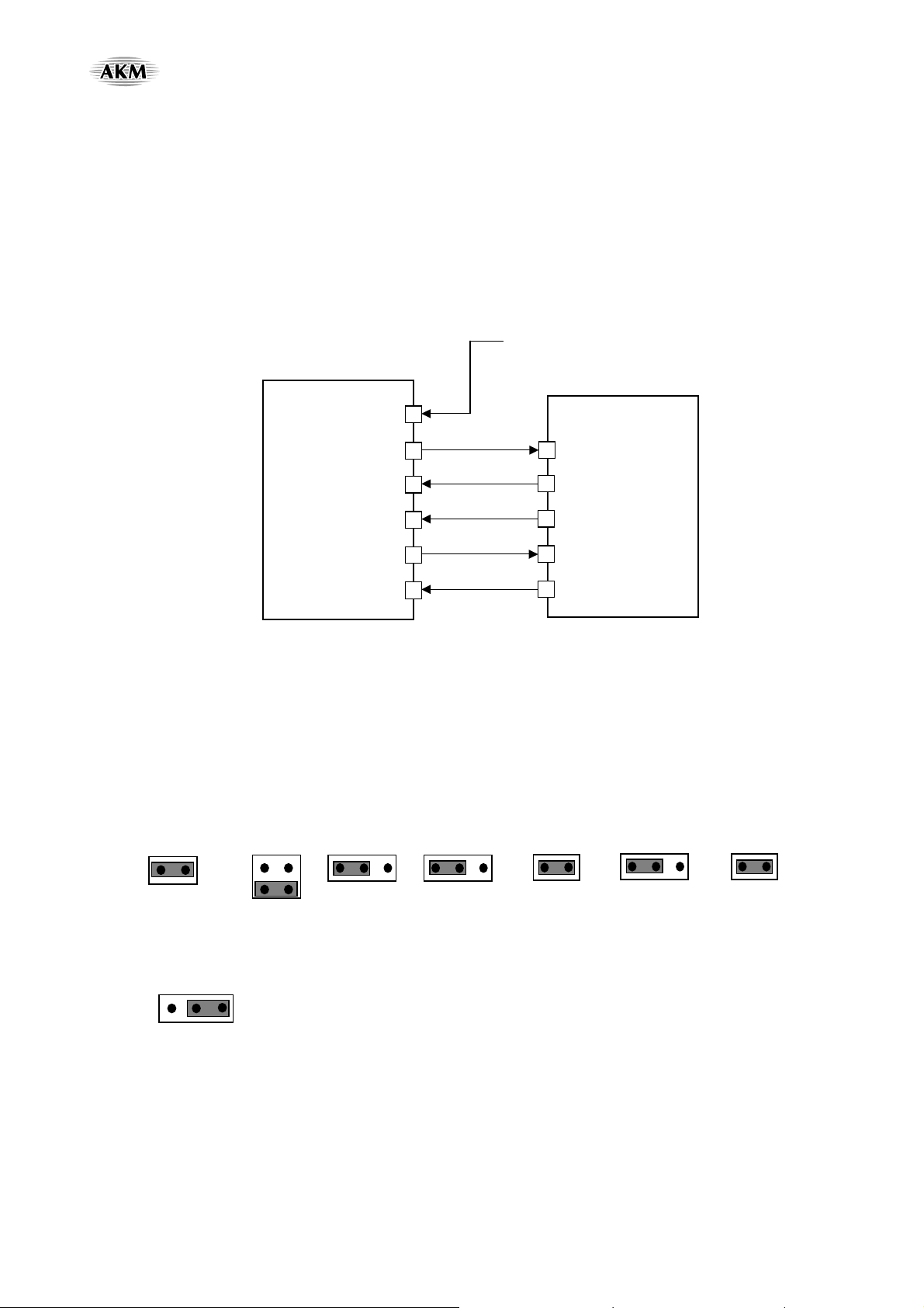
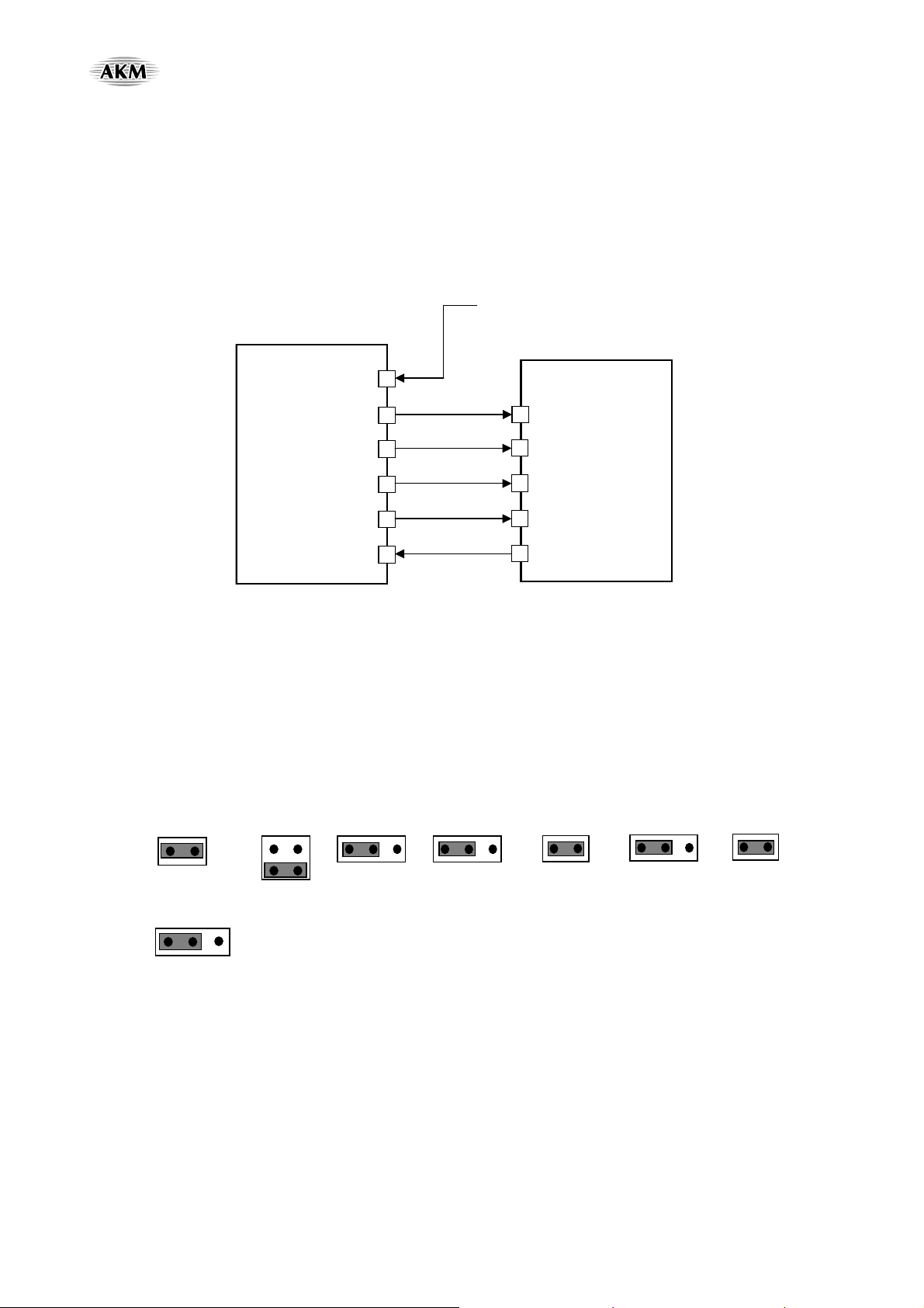
(1) External Slave Mode
When PMPLL bit is “0”, the AK4671 becomes EXT mode. Master clock is input from MCKI pin, the internal PLL
circuit is not operated. This mode is compatible with I/F of the normal audio CODEC. The clocks required to
operate are MCKI (256fs, 384fs, 512fs, 768fs or 1024fs), LRCK (fs) and BICK (≥32fs). The master clock (MCKI)
should be synchronized with LRCK. The phase between these clocks does not matter. The input frequency of MCKI
is selected by FS1-0 bits.
AK4671
DSP or μP
MCKI
BICK
LRCK
SDTO
SDTI
BCLK
LRCK
SDTI
SDTO
MCKO
1fs
≥32fs
MCLK
256fs, 384fs, 512fs,
768fs or 1024fs
(1-1)Evaluation of A/D using DIT of AK4114
X2 (X’tal) and PORT2 (DIT) are used. Nothing should be connected to PORT1 (DIR) and PORT4 (DSP).
The jumper pins should be set as the following.
(1-2) Evaluation of D/A using DIR of AK4114
PORT1 (DIR) is used. Nothing should be connected to PORT2 (DIT) and PORT4 (DSP).
The jumper pins should be set as the following.
JP36
MCLK
DI
R
EX
T
JP35
PHASE
IN
V
THR
JP38
LRCK_SEL
4040DIR
404
0
DIR
JP33
BICK_SEL JP46
4114_MCKI JP48
M/S
Slav
e
Master
JP36
MCLK
DI
R
EX
T
JP35
PHASE
IN
V
THR
JP38
LRCK_SEL
4040DIR
JP51
SDTI_SEL
ADCDIR
JP33
BICK_SEL
4040DIR
JP48
M/S
Slav
e
Master

[AKD4671-B]
<KM089001> 2008 / 03
- 8 -
(1-3) Evaluation of Loop-back using AK4114 <default>
X2 (X’tal) is used. Nothing should be connected to PORT1 (DIR), PORT2 (DIT) and PORT4 (DSP).
The jumper pins should be set as the following.
(1-4) Evaluation of Loop-back where master clock is fed externally, BICK and LRCK are generated by
on-board divider.
J12 (EXT) is used . MCLK is supplied from J12 (EXT). BICK and LRCK are generated by 74HC4040 on
AKD4671-B.
Nothing should be connected to PORT1 (DIR), PORT2 (DIT) and PORT4 (DSP).
The jumper pins should be set as the following.
When a termination (51Ω) is unnecessary, please set JP39 (EXT) open.
JP32 (MKFS), JP34 (BCFS), and JP37 (LRCK) should be set according to the frequency of MCLK, BICK and
LRCK.
Follows are setting examples in MCLK=256fs , BICK=64fs and LRCK=1fs.
When MCLK=384fs or 768fs, JP32, JP34, and JP37 should be set to “384” side.
.
(1-5) All interface signals including master clock are fed externally
PORT4 (DSP) is used. Nothing should be connected to PORT1 (DIR) and PORT2 (DIT).
The jumper pins should be set as the following.
JP36
MCLK
DI
R
EX
T
JP35
PHASE
IN
V
THR
JP38
LRCK_SEL
4040DIR
JP51
SDTI_SEL
AD
C
DIR
JP33
BICK_SEL
4040DIR
JP46
4114_MCKI JP48
M/S
SlaveMaster
JP36
MCLK JP33
BICK_SEL
404
0
DIR
DI
R
EX
T
JP38
LRCK_SEL
404
0
DIR
JP51
SDTI_SEL
AD
C
DIR
JP39
EXT JP48
M/S
Slav
e
Master
JP34
BCFS
JP32
MKFS
256fs
512fs
1024fs
384/768fs
MCK
O
64fs-384
32fs-384
64fs
32fs
JP37
LRCK
fs-384
fs
JP36
MCLK JP33
BICK_SEL
4040DIR
DI
R
EX
T
JP38
LRCK_SEL
4040DIR
JP51
SDTI_SEL
ADCDIR
JP48
M/S
Slav
e
Maste
[AKD4671-B]
<KM089001> 2008 / 03
- 9 -
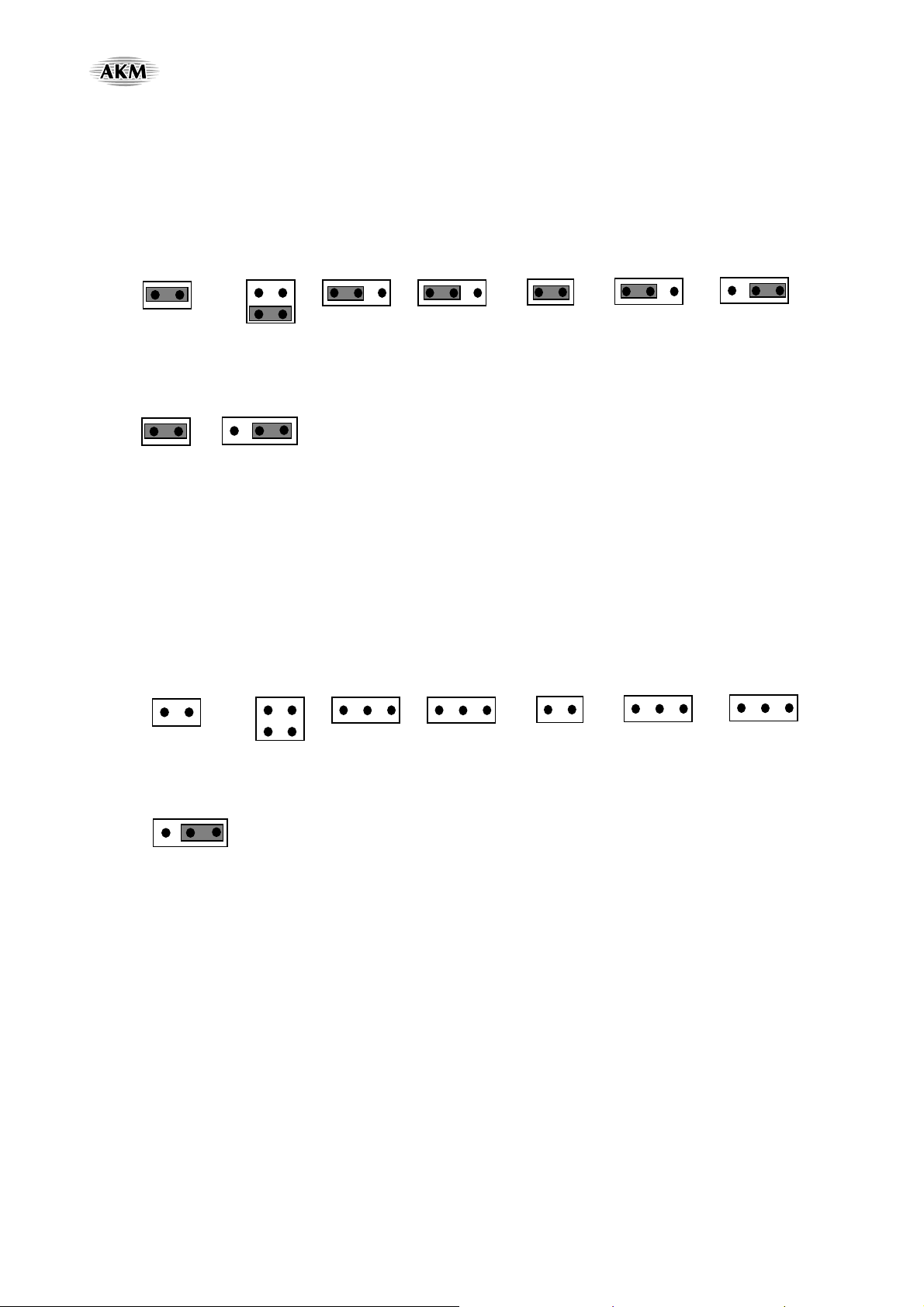
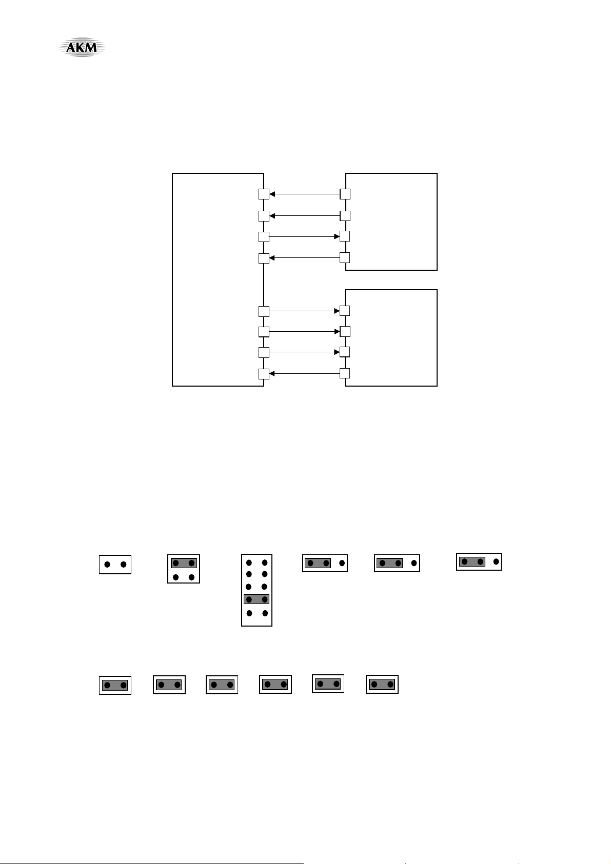
(2) External Master Mode
The AK4671 becomes EXT Master Mode by setting PMPLL bit = “0” and M/S bit = “1”. Master clock can be input
via MCKI pin, without using on-chip PLL circuit. The clock required to operate is MCKI (256fs, 384fs, 512fs,
768fs or 1024fs). The input frequency of MCKI is selected by FS1-0 bits.
AK4671
DSP or μP
MCKI
BICK
LRCK
SDTO
SDTI
BCLK
LRCK
SDTI
SDTO
MCKO
1fs
32fs or 64fs
MCLK
256fs, 384fs, 512fs,
768fs or 1024fs
(2-1)Evaluation of A/D using DIT of AK4114
X2 (X’tal) and PORT2 (DIT) are used. Nothing should be connected to PORT1 (DIR) and PORT4 (DSP).
In Master Mode, BICK and LRCK of AK4671 should be input to AK4114. Please refer to Table 2 on page 19.
The jumper pins should be set as the following.
(2-2) Evaluation of D/A using DIR of AK4114
PORT1 (DIR) is used. Nothing should be connected to PORT2 (DIT) and PORT4 (DSP).
In Master Mode, BICK and LRCK of AK4671 should be input to AK4114. Please refer to Table 2 on page 19.
The jumper pins should be set as the following.
JP36
MCLK
DI
R
EX
T
JP35
PHASE
IN
V
THR
JP38
LRCK_SEL
4040DIR
404
0
DIR
JP33
BICK_SEL JP46
4114_MCKI JP48
M/S
Slav
e
Master
JP36
MCLK
DI
R
EX
T
JP35
PHASE
IN
V
THR
JP38
LRCK_SEL
4040DIR
JP51
SDTI_SEL
ADCDIR
JP33
BICK_SEL
4040DIR
JP48
M/S
Slav
e
Master
[AKD4671-B]
<KM089001> 2008 / 03
- 10 -
(2-3) Evaluation of Loop-back using AK4114
X’tal (X2) is used. Nothing should be connected to PORT1 (DIR), PORT2 (DIT) and PORT4 (DSP).
The jumper pins should be set as the following.
(2-4) All interface signals including master clock are fed externally
PORT4 (DSP) is used. Nothing should be connected to PORT1 (DIR) and PORT2 (DIT).
The jumper pins should be set as the following.
JP36
MCLK
DI
R
EX
T
JP35
PHASE
IN
V
THR
JP38
LRCK_SEL
4040DIR
JP51
SDTI_SEL
AD
C
DIR
JP33
BICK_SEL
4040DIR
JP36
MCLK JP33
BICK_SEL
4040DIR
DI
R
EX
T
JP38
LRCK_SEL
4040DIR
JP51
SDTI_SEL
ADCDIR
JP48
M/S
Slav
e
Master
[AKD4671-B]
<KM089001> 2008 / 03
- 11 -
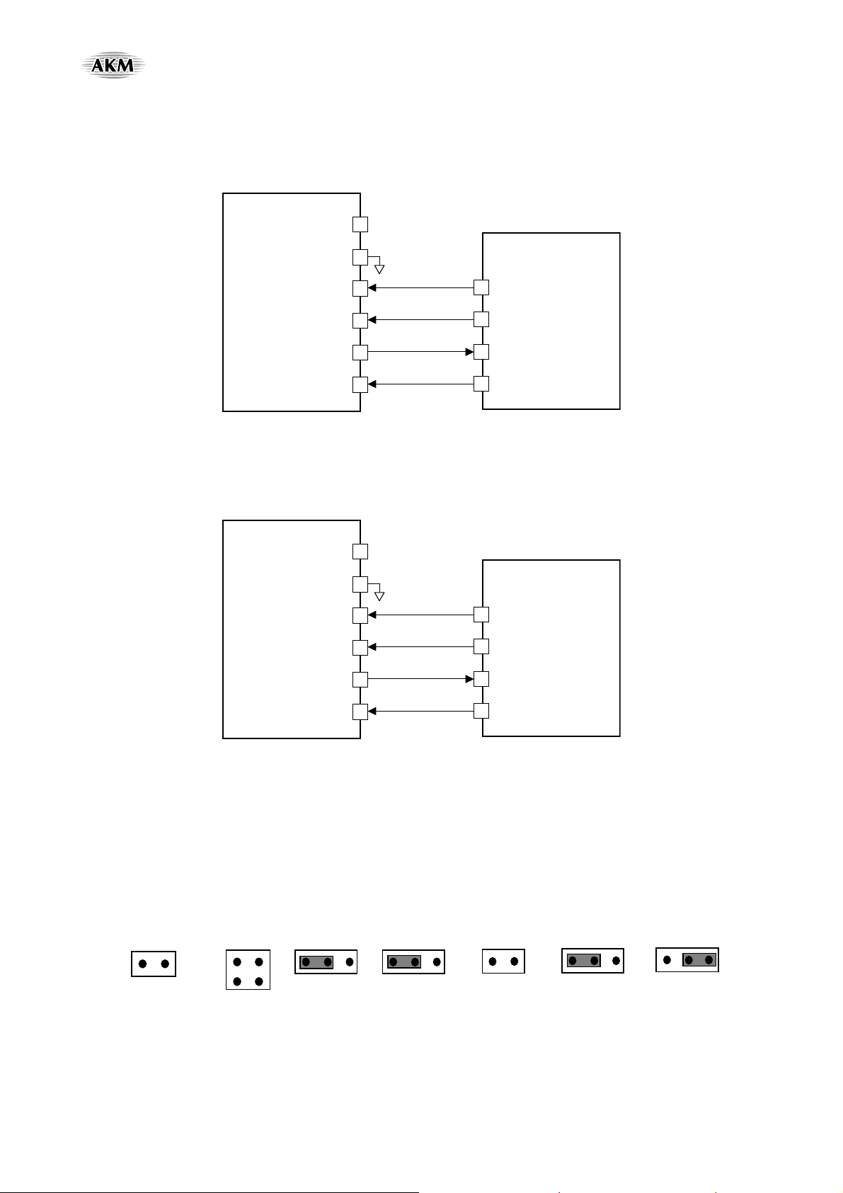
(3) PLL Slave Mode
A reference clock of PLL is selected among the input clocks to MCKI, BICK or LRCK pin. The required clock to
the AK4671 is generated by an internal PLL circuit. Input frequency is selected by PLL3-0 bits.
BICK and LRCK inputs should be synchronized with MCKO output. The phase between MCKO and LRCK dose
not matter. MCKO pin outputs the frequency selected by PS1-0 bits and the output is enabled by MCKO bit.
Sampling frequency can be selected by FS3-0 bits.
(3-1) PLL Reference Clock : MCKI pin
AK4671 DSP or μP
MCKO
BICK
LRCK
SDTO
SDTI
BCLK
LRCK
SDTI
SDTO
MCKI
1fs
≥32fs
MCLK
256fs/128fs/64fs/32fs
11.2896MHz, 12MHz, 12.288MHz, 13MHz,
13.5MHz, 19.2MHz, 24MHz, 26MHz,
27MHz
(3-1-1) Evaluation of A/D using DIT of AK4114
J12 (EXT) and PORT2 (DIT) are used. Nothing should be connected to PORT1 (DIR) and PORT4 (DSP).
X’tal oscillator should be removed from X2.
The jumper pins should be set as the following.
When a termination (51Ω) is unnecessary, please set JP39 (EXT) to open.
JP36
MCLK JP33
BICK_SEL
404
0
DIR
DI
R
EX
T
JP38
LRCK_SEL
404
0
DIR
JP39
EXT JP46
4114_MCKI JP35
PHASE
IN
V
THR
JP7
MCKO
JP48
M/S
SlaveMaster
[AKD4671-B]
<KM089001> 2008 / 03
- 12 -
(3-1-2) Evaluation of Loop-back using AK4114
J12 (EXT) is used. Nothing should be connected to PORT1 (DIR), PORT2 (DIT) and PORT4 (DSP).
X’tal oscillator should be removed from X2.
The jumper pins should be set as the following.
When a termination (51Ω) is unnecessary, please set JP39 (EXT) open.
(3-1-3) All interface signals including master clock are fed externally
PORT4 (DSP) is used. Nothing should be connected to PORT1 (DIR) and PORT2 (DIT).
The jumper pins should be set as the following.
JP36
MCLK JP33
BICK_SEL
404
0
DIR
DI
R
EX
T
JP38
LRCK_SEL
404
0
DIR
JP39
EXT JP46
4114_MCKI JP35
PHASE
IN
V
THR
JP51
SDTI_SEL
AD
C
DIR
JP7
MCKO JP48
M/S
Slave
Master
JP36
MCLK JP33
BICK_SEL
404
0
DIR
DI
R
EX
T
JP38
LRCK_SEL
404
0
DIR
JP39
EXT JP46
4114_MCKI JP35
PHASE
IN
V
THR
JP51
SDTI_SEL
AD
C
DIR
JP48
M/S
SlaveMaster
[AKD4671-B]
<KM089001> 2008 / 03
- 13 -
(3-2) PLL Reference Clock : BICK or LRCK pin
AK4671
DSP or μP
MCKI
BICK
LRCK
SDTO
SDTI
BCLK
LRCK
SDTI
SDTO
MCKO
1fs
32fs or 64fs
(PLL Reference Clock: BICK pin)
AK4671
DSP or μP
MCKI
BICK
LRCK
SDTO
SDTI
BCLK
LRCK
SDTI
SDTO
MCKO
1fs
≥32fs
(PLL Reference Clock: LRCK pin)
(3-2-1) Evaluation of A/D using DIT of AK4114
X2 (X’tal) and PORT2 (DIT) are used. Nothing should be connected to PORT1 (DIR) and PORT4 (DSP).
The jumper pins should be set as the following.
JP36
MCLK JP33
BICK_SEL
404
0
DIR
DI
R
EX
T
JP38
LRCK_SEL
404
0
DIR
JP39
EXT JP46
4114_MCKI JP35
PHASE
IN
V
THR
JP48
M/S
Slav
e
Maste
r
[AKD4671-B]
<KM089001> 2008 / 03
- 14 -
(3-2-2) Evaluation of D/A using DIR of AK4114
PORT1 (DIR) is used. Nothing should be connected to PORT2 (DIT) and PORT4 (DSP).
The jumper pins should be set as the following.
(3-2-3) Evaluation of Loop-back using AK4114
X2 (X’tal) is used. Nothing should be connected to PORT1 (DIR), PORT2 (DIT) and PORT4 (DSP).
The jumper pins should be set as the following.
(3-2-4) All interface signals including master clock are fed externally
PORT4 (DSP) is used. Nothing should be connected to PORT1 (DIR) and PORT2 (DIT).
The jumper pins should be set as the following.
JP36
MCLK JP33
BICK_SEL
404
0
DIR
DI
R
EX
T
JP38
LRCK_SEL
404
0
DIR
JP39
EXT JP46
4114_MCKI JP35
PHASE
IN
V
THR
JP51
SDTI_SEL
AD
C
DIR
JP48
M/S
SlaveMaster
JP36
MCLK JP33
BICK_SEL
404
0
DIR
DI
R
EX
T
JP38
LRCK_SEL
404
0
DIR
JP39
EXT JP46
4114_MCKI JP35
PHASE
IN
V
THR
JP51
SDTI_SEL
AD
C
DIR
JP48
M/S
SlaveMaster
JP36
MCLK JP33
BICK_SEL
404
0
DIR
DI
R
EX
T
JP38
LRCK_SEL
404
0
DIR
JP39
EXT JP46
4114_MCKI JP35
PHASE
IN
V
THR
JP51
SDTI_SEL
AD
C
DIR
JP48
M/S
SlaveMaster
[AKD4671-B]
<KM089001> 2008 / 03
- 15 -
(4) PLL Master Mode
When an external clock (11.2896MHz, 12MHz, 12.288MHz, 13MHz, 13.5MHz, 19.2MHz, 24MHz, 26MHz or
27MHz) is input to MCKI pin, the MCKO, BICK and LRCK clocks are generated by an internal PLL circuit. The
MCKO output frequency is selected by PS1-0 bits and the output is enabled by MCKO bit. The BICK output
frequency is selected between 32fs or 64fs, by BCKO bit.
AK4671 DSP or μP
MCKO
BICK
LRCK
SDTO
SDTI
BCLK
LRCK
SDTI
SDTO
MCKI
1fs
32fs, 64fs
256fs/128fs/64fs/32fs
11.2896MHz, 12MHz, 12.288MHz, 13MHz,
13.5MHz, 19.2MHz, 24MHz, 26MHz,
27MHz
MCLK
(4-1)Evaluation of A/D using DIT of AK4114
J12 (EXT) and PORT2 (DIT) are used. Nothing should be connected to PORT1 (DIR) and PORT4 (DSP).
X’tal oscillator should be removed from X2.
In Master Mode, BICK and LRCK of AK4671 should be input to AK4114. Please refer to Table 2 on page 19.
The jumper pins should be set as the following.
When a termination (51Ω) is unnecessary, please set JP39 (EXT) open.
JP36
MCLK JP33
BICK_SEL
404
0
DIR
DI
R
EX
T
JP38
LRCK_SEL
404
0
DIR
JP39
EXT JP46
4114_MCKI JP35
PHASE
IN
V
THR
JP7
MCKO
JP48
M/S
SlaveMaster
[AKD4671-B]
<KM089001> 2008 / 03
- 16 -
(4-2) Evaluation of Loop-back
J12 (EXT) is used. Nothing should be connected to PORT1 (DIR), PORT2 (DIT) and PORT4 (DSP).
X’tal oscillator should be removed from X2.
The jumper pins should be set as the following.
When a termination (51Ω) is unnecessary, please set JP39 (EXT) open.
(4-3) All interface signals including master clock are fed externally
PORT4 (DSP) is used. Nothing should be connected to PORT1 (DIR) and PORT2 (DIT).
The jumper pins should be set as the following.
JP36
MCLK JP33
BICK_SEL
404
0
DIR
DI
R
EX
T
JP38
LRCK_SEL
404
0
DIR
JP39
EXT JP46
4114_MCKI JP3
5
PHASE
IN
V
THR
JP51
SDTI_SEL
AD
C
DIR
JP48
M/S
SlaveMaster
JP36
MCLK JP33
BICK_SEL
404
0
DIR
DI
R
EX
T
JP38
LRCK_SEL
404
0
DIR
JP39
EXT JP46
4114_MCKI JP3
5
PHASE
IN
V
THR
JP51
SDTI_SEL
AD
C
DIR
JP48
M/S
SlaveMaster

[AKD4671-B]
<KM089001> 2008 / 03
- 17 -
2. PCM I/F evaluation mode
A reference clock of PLLBT is selected among the input clocks to SYNCA, BICKA, SYNCB or BICKB pin.
The required clock to PCM I/F is generated by an internal PLLBT circuit. PLLBT circuit is powered up by
PMPCM bit. Input frequency is selected by PLLBT2-0 bits. BCKO2 bit select the output clock frequency of
BICKA or BICKB pin.
AK4671 does not support master mode for both PCM I/F A and B nor slave mode
for both PCM I/F A and B. When PMPCM bit is “0”, SYNCA, BICKA, SYNCB and BICKB pins are Hi-Z.
(1) PLLBT reference clock: SYNCA or BICKA pin
(1-1)SYNCA and BICKA are fed from on-board clock generator.
(1-2) SYNCA and BICKA are fed externally via PORT3 (Baseband Module).
(2) PLLBT reference clock: SYNCB or BICKB pin
(2-1)SYNCB and BICKB are fed from on-board clock generator.
(2-2) SYNCB and BICKB are fed externally via PORT6 (Bluetooth Module).
[AKD4671-B]
<KM089001> 2008 / 03
- 18 -
(1) PLLBT reference clock: SYNCA or BICKA pin
The PLLBT circuit generates the required clock for PCM I/F from SYNCA or BICKA. Generated clocks are output
via SYNCB and BICKB pins.
A
K4671 Baseband Module
BICKA
SDTOA
SDTIA
SYNCB
SDTI
SDTO
SYNC
SYNCA 1fs2
≥16fs2 BICK
BICKB
SDTOB
SDTIB
SDTI
SDTO
1fs2
16fs2 or 32fs2 BICK
SYNC
Bluetooth Module
(PLLBT Reference Clock: SYNCA or BICKA pin)
(1-1)SYNCA and BICKA are fed from on-board clock generator.
X1 (X’tal), PORT3 (Baseband Module) and PORT6 (Bluetooth Module) are used.
The jumper pins should be set as the following.
Please set JP42 (BCFS2) to the required frequency. Follows are setting in BICKA=32fs.
When clocks are supplied from J13 (EXT1) without using X1, JP41 (MCLK2) should be set to “EXT1”.
JP41
MCLK2
XT
L
EXT1
JP43
BICK2_SEL
BICKBBICKA
JP40
XTE JP42
BCFS2 JP49
PLLBT
BICK
B
BICKA
256fs2
128fs2
64fs2
32fs2
16fs2
JP45
LRCK2_SEL
LRCKBLRCKA
JP62
BICKA JP63
SYNCA JP64
BICKB JP65
SYNCB JP61
SDTIB JP60
SDTIA

[AKD4671-B]
<KM089001> 2008 / 03
- 19 -
JP47 (BICKA PHASE) is jumper which decides polarity of BICKA, “THR” or “INV” should be selected
according to the PCM I/F format.
JP54 (BICKB PHASE) should be set to “THR”.
In case of loop-back “SDTOA →SDTIA” and “SDTOB →SDTIB”, please set JP50 (SDTOA LOOP) and
JP55 (SDTOB LOOP) short.
(1-2) SYNCA and BICKA are fed externally via PORT3 (Baseband Module).
PORT3 (Baseband Module) and PORT6 (Bluetooth Module) are used.
SYNCA and BICKA should be supplied from PORT3.
The jumper pins should be set as the following.
JP47 (BICKA PHASE) is jumper which decides polarity of BICKA, “THR” or “INV” should be selected
according to the PCM I/F format.
JP54 (BICKB PHASE) should be set to “THR”.
JP47
BICKA PHASE
IN
V
THR
JP54
BICKB PHASE
IN
V
THR
JP50
SDTOA LOOP JP55
SDTOB LOOP
JP41
MCLK2
XT
L
EXT1
JP43
BICK2_SEL
BICKBBICKA
JP40
XTE JP49
PLLBT
BICK
B
BICKA
JP45
LRCK2_SEL
LRCKBLRCKA
JP47
BICKA PHASE
IN
V
THR
JP54
BICKB PHASE
IN
V
THR

[AKD4671-B]
<KM089001> 2008 / 03
- 20 -
(2) PLLBT reference clock: SYNCB or BICKB pin
The PLLBT circuit generates the required clock for PCM I/F from SYNCB or BICKB. Generated clocks are output
via SYNCA and BICKA pins.
A
K4671 Baseband Module
BICKA
SDTOA
SDTIA
SYNCB
SDTI
SDTO
SYNC
SYNCA 1fs2
16fs2 or 32fs2 BICK
BICKB
SDTOB
SDTIB
SDTI
SDTO
1fs2
≥16fs2 BICK
SYNC
Bluetooth Module
(PLLBT Reference Clock: SYNCB or BICKB pin)
(2-1)SYNCB and BICKB are fed from on-board clock generator.
X1 (X’tal), PORT3 (Baseband Module) and PORT6 (Bluetooth Module) are used.
The jumper pins should be set as the following.
Please set JP42 (BCFS2) to the required frequency. Follows are setting in BICKB=32fs.
When clocks are supplied from J13 (EXT1) without using X1, JP41 (MCLK2) should be set to “EXT1”.
JP62
BICKA JP63
SYNCA JP64
BICKB JP65
SYNCB JP61
SDTIB JP60
SDTIA
JP41
MCLK2
XT
L
EXT1
JP43
BICK2_SEL
BICKBBICKA
JP40
XTE JP42
BCFS2 JP49
PLLBT
BICK
B
BICKA
256fs2
128fs2
64fs2
32fs2
16fs2
JP45
LRCK2_SEL
LRCKBLRCKA
Table of contents
Other ASAHI Motherboard manuals


