DAQ system USB-EK01 User manual

http://www.daqsystem.co
m
USB-EK01 Users Manual (Rev 1.0)
- 1 -
USB-EK01
User Manual
AN2131, EZ-USB and Cypress are trademarks of Cypress Semiconductor, Keil and uVision2 are trademarks of
Keil software. Windows, Windows2000, Windows NT and Windows XP are trademarks of Microsoft. We
acknowledge that the trademarks or service names of all other organizations mentioned in this document as their
own property.
The information in this document is subject to change without notice and no part of this document may be copied
or reproduced without the prior written consent.
Copyrights 2005 DAQ system, All rights reserved.

http://www.daqsystem.co
m
USB-EK01 Users Manual (Rev 1.0)
- 2 -
Contents
1. Introduction
2. USB-EK01 Function & Specification
3. Installation
3.1 Confirm Product Contents
3.2 Cypress Development kit Installation
3.3 Board Driver Installation
4. USB-EK01 Description
4.1 USB-EK01 Concept
4.2 Memory Map
4.2.1 EK01 Memory map
4.2.2 IK01 Memory Map
4.3 Booting Option
4.4 CDROM Folder
5. Test
5.1 Example
5.2 Program & Debugging with KeiluVision
5.3 USB Firmware
5.4 Make USB PC Driver
5.5 Make EEPROM Image
5.6 Application Program for PC
Appendix
A Driver Installation & Remove
B Board connector PIN map
C Notice
Reference

http://www.daqsystem.co
m
USB-EK01 Users Manual (Rev 1.0)
- 3 -
1. Introduction
SW1
SW2
SW3
JP5
(USB B type
Connector)
DAQ system
D1 D2 D3
JP1(Boare Extention)
JP7(Boare Extention)
P1
RS232
connection
JP4
JP6
JP3
JP2
AN2131
D4
www.daqsystem.com
Reset
Power
[Figure 1-1. USB-EK01 Out-side View]
Above picture views board out-side, it display Reset switch and Power LED which
light on when power supply with connection cable. More specific information refer to
“4.1 USB-EK01 Concept”.

http://www.daqsystem.co
m
USB-EK01 Users Manual (Rev 1.0)
- 4 -
2. USB-EK01 Function & Specification
<Function>
- USB Protocol Test & Development
- 8051 Program Test & Development
- PC용USB device driver Test & Development
- Step by Step Debugging Practice
<Specification>
- Full speed (12Mbps) USB Support
- Advanced using 8051 core Micro-Controller
- Convenient Interface USB SIE (Serial Interface Engine)
- Step by Step Debugging & 8051 Compile Test (Code size limited 4K)
- Power Supply through USB Cable (Max. 500mA)
- Two RS232 interface (Maximum transfer speed-115200bps) Debugging or
It can use special purpose.
- Board Reset & Firmware Program Load through USB
- Easy device development through Cypress의Development Kit
- Usable evaluation Keil Compiler & Debugger (Limit 4K code)

http://www.daqsystem.co
m
USB-EK01 Users Manual (Rev 1.0)
- 5 -
3. Installation
3.1 Confirm Product Contents
[Figure 3-1. USB-EK01 Main Contents]
(1) USB-EK01 Evaluation board
(2) USB (A-B) Cable
(3) 9Pin Null Modem cable
(4) CD (Manual/Schematic/Sample test etc..)
3.2. Cypress Development kit Installation
A development and exercise of board refer to mainly Development Kit at Cypress,
you can get a lot of information and report. You can use the ”Development kit”to
download at homepage of Cypress. (“www.cypress.com”) The “Development kit “is a
software package minimum 60Mbyte size, If it install, the folder structure is as follows.

http://www.daqsystem.co
m
USB-EK01 Users Manual (Rev 1.0)
- 6 -
[Figure 3-2. Folder Structure]
[Notice] If you want a Keil software and separate reference report, you shall select a
custom install option not default.
You confirm a folder at your PC as above picture when normally finished install.
The Cypress Development Kit include Keil compiler and debugger, you can freely use
a code size of 4K byte in range not business purpose.

http://www.daqsystem.co
m
USB-EK01 Users Manual (Rev 1.0)
- 7 -
3.3 Board Driver Installation
(Notice) All test made a Windows2000 Professional with bases, we are having finished
the final test at Windows XP.
Execute “Device Manager”at My Computer -> Properties -> Hardware -> Device
Manager window.
[Figure 3.3 Select “My computer”->”Properties”]
[Figure 3.4 “Device Manager” window]

http://www.daqsystem.co
m
USB-EK01 Users Manual (Rev 1.0)
- 8 -
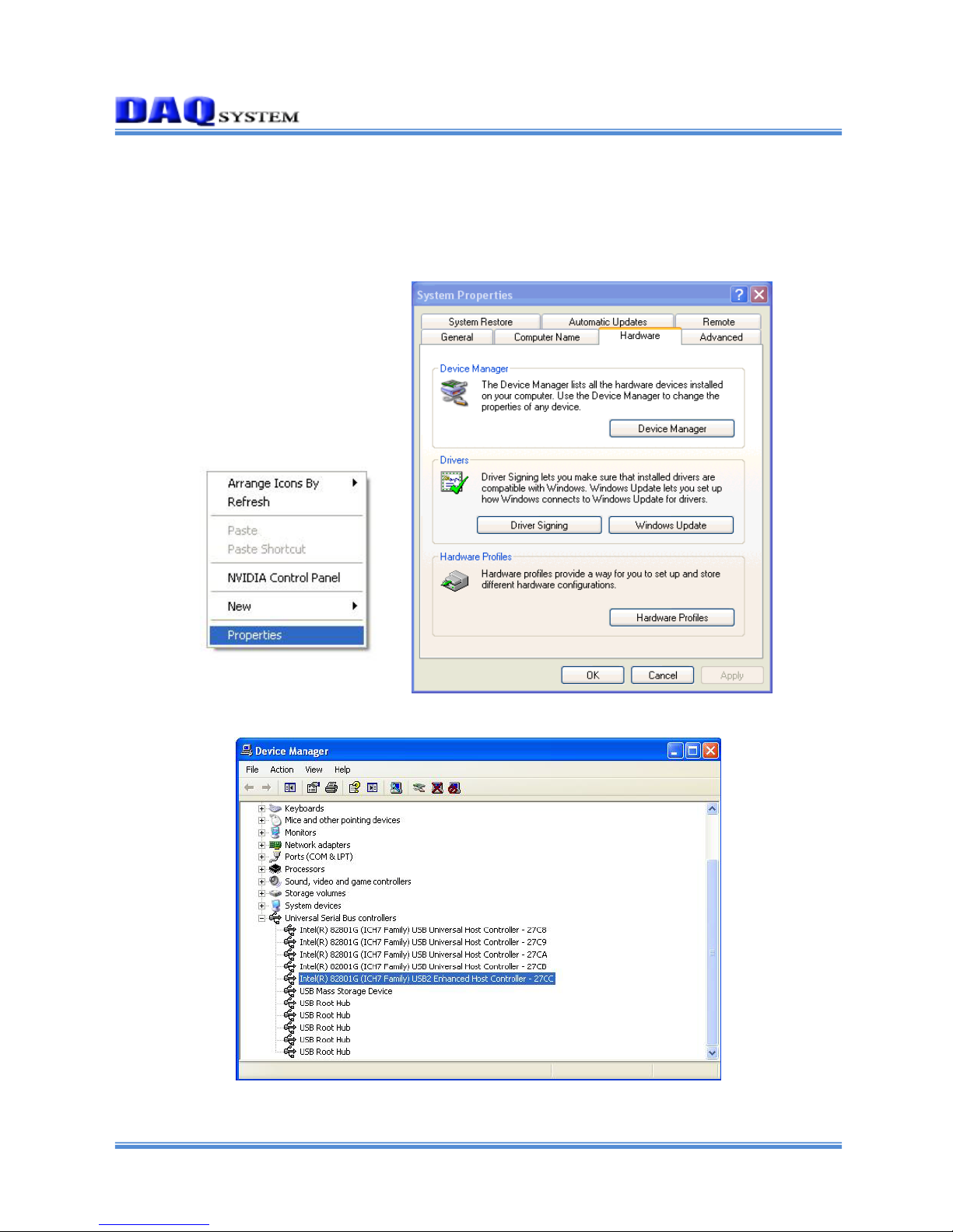
Figure 3.4 shows that “Device Manager”execution window. You can check all USB
device connection at your PC. Currently not yet connect “USB-EK01”, it is not
marked.
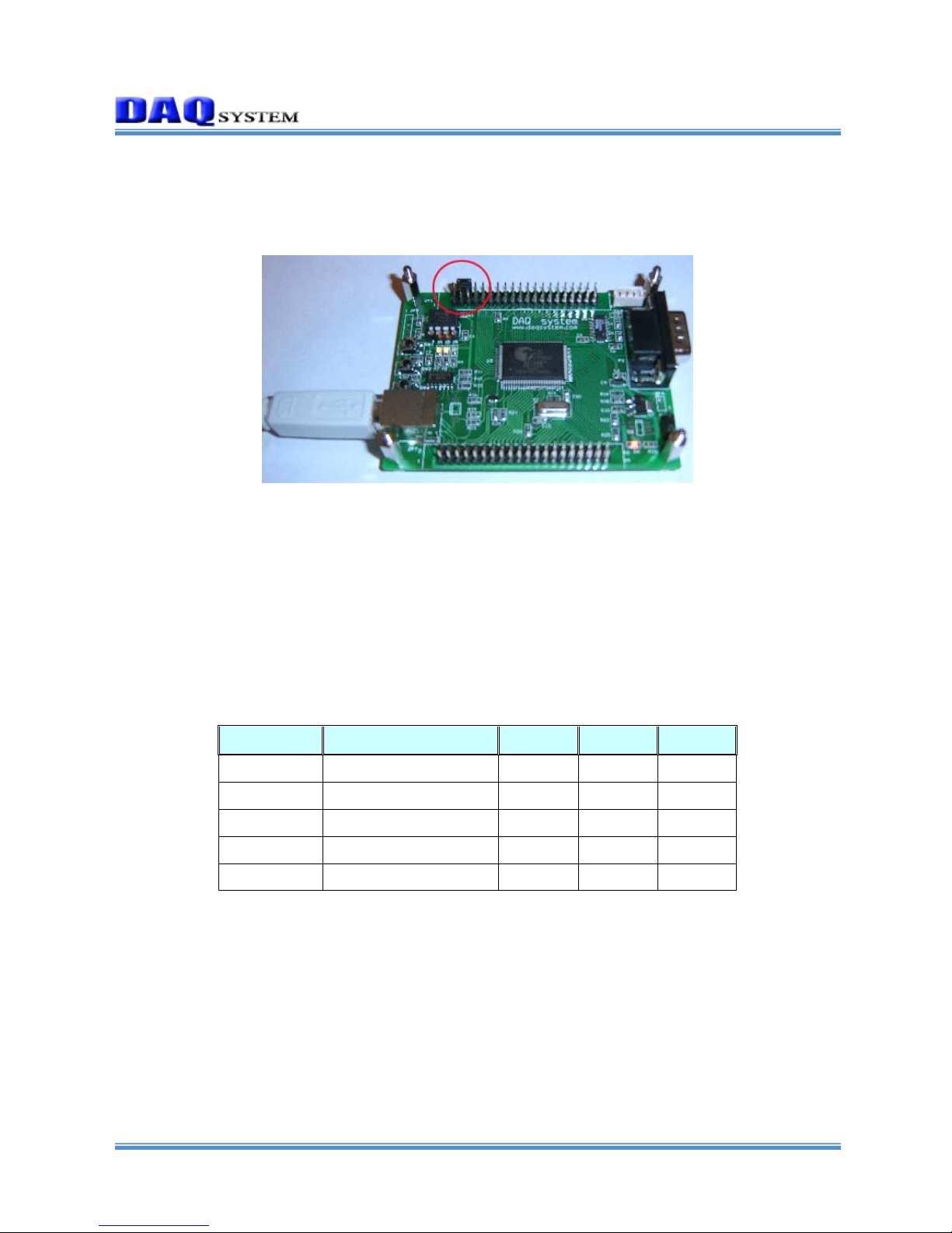
[Figure 3.5 USB-EK01 Connection]
The USB-EK01 is connected to PC through USB cable after jumper setting like
above red circle. The reason of using jumper is that an address of EEPROM(24LC64)
is able to recognize it at AN2131. AN2131 is having function of EEPROM information
to connect I2C port can select a lot of booting option when Power On Booting.
Usable EEPROM is same as the following table to a board booting option. Refer to
“I2C Boot Loader”of AN2131 manual for special information.
Bytes EEPROM A2 A1 A0
16 24LC00 N/A N/A N/A
128 24LC01 0 0 0
256 24LC02 0 0 0
4K 24LC32 0 0 1
8K 24LC64 0 0 1
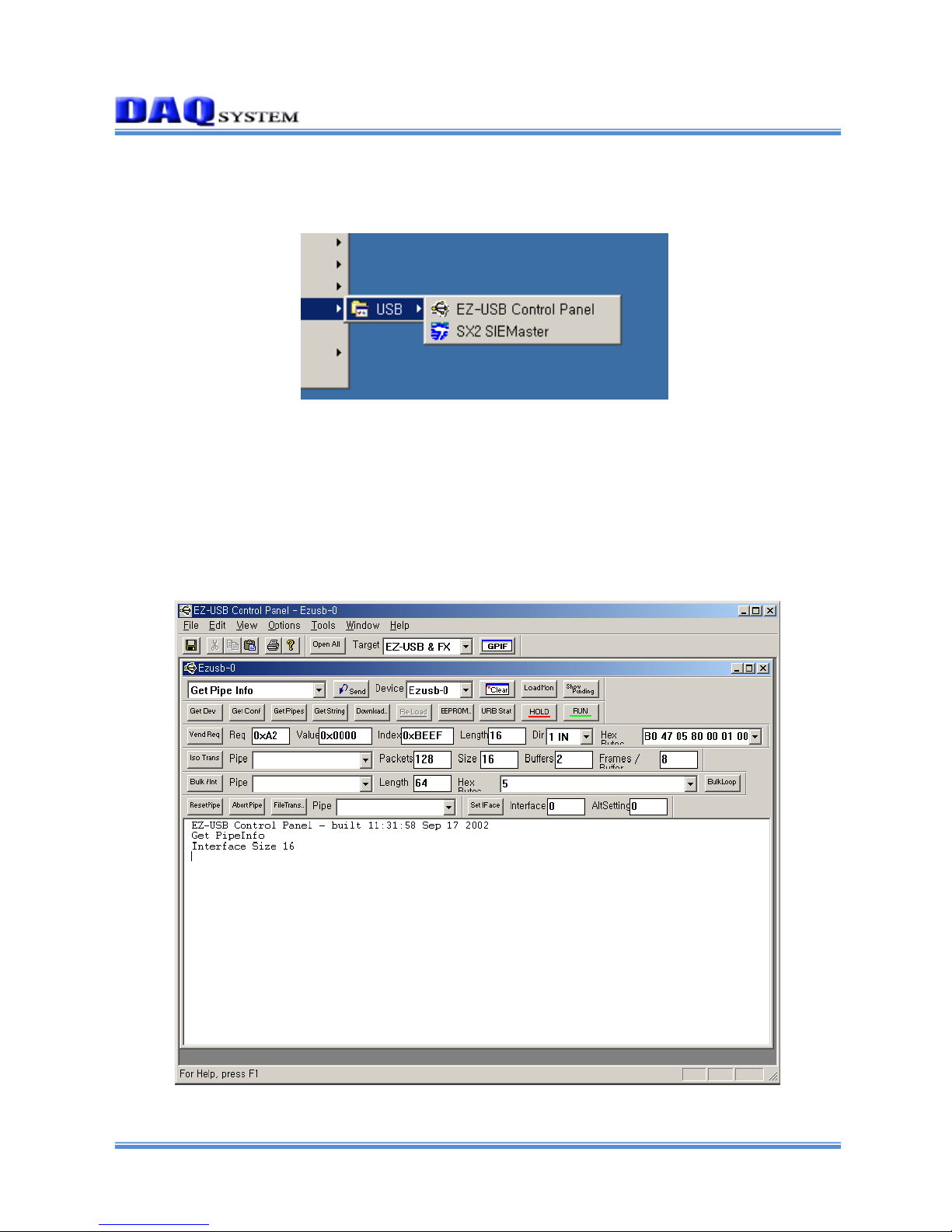
When it is connected to USB cable, “New Hardware Search Wizard”execute
automatically, you can check the USB device at “Device Manager”.
It don’t require another driver because of Cypress Development Kit was installed.
Figure 3.6 will be shown after completely installation. An EEPROM information of board
is as follows at default (when first purchase).
0000h: B0 47 05 80 00 00 00 (Refer to file 2100.iic at Cypress)
That is, Using VID(Vender ID) = 0x547, PID(Product ID)=0x80 in EEPROM will be
registered to PC in an USB device.

http://www.daqsystem.co
m
USB-EK01 Users Manual (Rev 1.0)
- 9 -
[Figure 3.6 A board was registered with default to PC]
If the jumper don’t connect, the screen is as follows. The way that you can confirm,
after remove jumper, reset switch of a board is “ON/OFF”or reconnect a USB cable
after remove. For more specific information, refer to “Chapter 4.3 Booting Option”.
[Figure 3.7 A board was registered to PC without recognition EEPROM]

http://www.daqsystem.co
m
USB-EK01 Users Manual (Rev 1.0)
- 10 -
You confirm to register to PC like figure 3.6 that rebooting a board after connection
jumper. After that, “EZ-USB Control Panel(EzMr.exe)”utility which given Cypress
Development Kit perform.
[Figure 3.8 EZ-USB Control Panel]
(Notice) When development a product at Cypress, Usable utility is searchable in
“Cypress\USB \Bin”and “Cypress\USB\Util”.
The execution screen of “EZ-USB Control Panel(EzMr.exe)”is like figure 3.9.
If connection doesn’t work a device, the error message will be marked.
[Figure 3.9 EZ-USB Control Panel]

http://www.daqsystem.co
m
USB-EK01 Users Manual (Rev 1.0)
- 11 -
For more usage method of Control Panel, refer to “EZ-USB Contents and tutorial.pdf”
at Cypress.
From now, the board installs to a “DAQ system”development board so that
registration works to PC. Basically all test above setting even is possible, a driver of
DAQ system shall be install in case of the debugging that used Keil software in order to
put a necessary image to a board. The Vender ID which used to installation is “FFFF”,
this is not the ID which it was registered and I used it as I select temporary.
When Power On Reset, it will act to any contents and a report judges the contents as
reading the first byte of EEPROM connected to I2C.
If the first byte is not ‘0xB0’or ‘0xB2’, it is performed with default as judge it to
things without EEPROM. (Vender ID 0x0547, Product ID 2131).
It shall modify contents of EEPROM so that recognition gets a board done to a
development board of DAQ system. (Vender ID 0xFFFF, Product ID 0001)
For more detailed egarding boot option, refer to “Chapter 4.3 Booting Option”.
A way to modify of EEPROM is as follows.
When press “EEPROM”button at EZ-USB Control Panel, “file dialogue box”appears.
When it is selected a file “Sample.eep”of Program\EPROM_IMG folder in CDROM and
press open button, will be changed a contents of EEPROM.
[Figure 3.10 “sample.eep”for changing EEPROM’s information]

http://www.daqsystem.co
m
USB-EK01 Users Manual (Rev 1.0)
- 12 -
The contents that it was changed are as follows.
0000h: B0 FF FF 01 00 00 00, in other words, VID is 0xFFFF and PID is 0x0001.
When finished EEPROM writing, press reset switch or remove and re-connect the USB
cable. The board gets re-registration at PC.
And then, above ID doesn’t currently get registration at PC, “New Hardware Search
wizard”will be open and display like figure 3.11.
[Figure 3.11 New Hardware search Wizard Window]
Press “Next”button.

http://www.daqsystem.co
m
USB-EK01 Users Manual (Rev 1.0)
- 13 -
[figure 3.12 Driver Installation Window]
Press “Next”button.
[Figure 3.13 Driver File Search Window]
After select a location like above figure, press “Next”button.

http://www.daqsystem.co
m
USB-EK01 Users Manual (Rev 1.0)
- 14 -
[Figure 3.14 Driver Selection window]
After select a file “daqusbw2k.inf”in Software\Driver folder at CDROM, press
“Confirm”button and will finish driver installation. If installation finish, press “finish”
button and disappear window like figure 3.15.
[Figure 3.15 Driver Installation Completion window]
If installation finish, you confirm a registration state that you perform “regedit.exe”at
Window. All contents registered to OS(Windows) that is saving to PC, stored contents
and revised program that can edit it is an registry editor(regedit.exe).

http://www.daqsystem.co
m
USB-EK01 Users Manual (Rev 1.0)
- 15 -
At display of “Start/Execution”, write “regedit”and press “Confirm”button.
[Figure 3.16 “Start/Execution”Window]
[Figure 3.17 Registry Editor Window]
If a registry editor is used most a case, it use to confirm and erase a value of key.
(Notice)If a key value want erase, it can erase it at “Security”items as it perform
regedit32 after having exchanged use authority in case of Windows2000.
This concludes all installation procedure of test and development.

http://www.daqsystem.co
m
USB-EK01 Users Manual (Rev 1.0)
- 16 -
4. USB-EK01 Description
4.1 USB-EK001 Concept
A basic concept of USB-EK001 made it so that a hardware and software engineer
developed it so as to easily make various tests, and an engineer of various levels can
utilize it. In other words, a person to touch a embedded program and hardware for the
first time, the person whom he/she is familiar with other microcontroller, and want to
practice 8051 programming, embedded USB board Firmware development, USB device
driver development for PC, Application Programming through using USB interface at PC,
and we made it to use debugging practice step by step when embedded firmware
development. User can test all functions only using the USB-EK01 board, all
development tools can use it to free or evaluation type. Also, you can easily use because
you don’t need special power supply.
Now I will explain main connection and functions of USB-EK01 board.
SW1
SW2
SW3
JP5
(USB B type
Connector)
USB-EK01 Board
D1 D2 D3
JP1(Boare Extention)
JP7(Boare Extention)
P1
RS232
connection
JP4
JP6
JP3
JP2
AN2131
D4
[Figure 4.1 USB-EK01 Out-side View]

http://www.daqsystem.co
m
USB-EK01 Users Manual (Rev 1.0)
- 17 -
[Table 4.1 USB-EK01 Function Description]
No. Name Description
1 SW1 General Purpose Input
2 SW2 General Purpose Input
3 SW3 Reset
4 D1 General Purpose Output
5 D2 General Purpose Output
6 D3 Program Break Output
7 D4 Power Lamp
8 JP1 Address/Data/ I/O extension connector
9 JP2 Extension RS232 Interface(COM2)
10 JP3 Extension I2C Interface
11 JP4 Extension power connector.
It can use to connect
external power supply in case of power need a more
than 500mA.
12 JP5 USB B type connector (Host connection)
13 JP6 Power selection connector(It select a power whether
get from the power at USB cable or external electric
power supply banner.)
14 JP7 Address/Data/ I/O extension connector
15 P1 RS232C connection, it can
use a debugging and
general communication to maximum 115200bps.
Figure 4.2 shows USB-EK01 functional block diagram, we put emphasis to
expansibility and a design was performed around the main AN2131QC chip. All Data,
Address, I/O can exchange a board expansion, can connect external device through
RS232C, USB, I2C interface.
We made it so as there was a LED and Tact switch, and to be able to test the simple
external input/output test automatically, and don’t need an external power supply
because basically power supply get from USB cable.

http://www.daqsystem.co
m
USB-EK01 Users Manual (Rev 1.0)
- 18 -
USB
USB-EK001
Switchs
and
LEDs
Board Expantion
RS232
P/S JP3
AN2131
T/RxD
I/O
JP4
Addr, Data, I/O
+5V
+5V
COM1
COM1
I2C
USB
+3.3V
D+/-
EEPROM
+5V
Addr, Data, I/O
SCL/SDA
[Figure 4.2 USB-EK01 Functional Block Diagram]

http://www.daqsystem.co
m
USB-EK01 Users Manual (Rev 1.0)
- 19 -
4.2 Memory Map
4.2.1 USB-EK01(8051) Memory Map
Figure 4.3 shows general 8051 Microcontroller memory structure.
The 8051 is equipped with a memory which display inside dotted line, it is
different from memory which it use external data/address bus.
0xFFFF
XDATA
8051 Internal
CODE
IDATA
REGs
SFR
BDATA
DATA
0x0000
[Figure 4.3 8051 Memory Map]
An area to be possible to direct addressing methods in the inside is from 0x00 to
0x7F, address from 0x00 to 0x1F is used to the register bank(0 ~ 3) which it is used
when it operate at CPU. BDATA is from 0x20 to 0x2F, is able to the addressing in a
bit unit. From 0x80 to 0xFF of address is SFR(Special Function Register) area when
access to direct addressing methods, is general data area(IDATA) when access to
indirect addressing methods. The SFR area has the registers for CPU calculation and
for control surrounding I/O area.
8051 has separate space of the data memory area(XDATA) and the program
memory area(CODE), each area accessing classify to signal line of “RD/WR”and
“PSEN”. The program memory (CODE) can include in chip oneself, each
manufacturing company is able to choose various selection until the maximum 64K
Byte at 4K Byte. A mainly flash memory uses in now, user prefer that it is able to
exchange a structure of program. At this time, an input state of “EA”pin decides
whether or not there is to use an external memory whether or not there is to use
inner memory.

http://www.daqsystem.co
m
USB-EK01 Users Manual (Rev 1.0)
- 20 -
4.2.2 USB-EK01(AN2131) Memory Map
Cypress의AN2131 which have a core of 8051 microcontroller is same memory
structure of 8051 internal memory. But, other point got separate RAM(8K Byte) in
the chip inside and use to program and data memory.
Also, the RAM can use a EndPoint buffer in case of USB data transmission,
therefore, the driver write a program in this RAM area when first Power ON reset
and can make it so that a program operates that user wanted it.
The USB-EK01 board doesn’t have special external memory (RAM/ROM), it is
same structure of memory map like AN2131 chip.
0xFFFF
XDATA/
CODE
6,976 Bytes
EA = 0
AN2131QC Internal
IDATA
REGs
SFR
BDATA
DATA
0x0000
REGs/Buffers
DATA
REGs/Buffers
0x1B3F
0x1B40
0x1FFF
0x2000
0x27FF
0x7B40
0x7FFF
16x64
Bulk
End points
(1024 Bytes)
USB control
registers
192 Bytes
[Figure 4.4 USB-EK01(AN2131) Memory Map]
But, if the USB-EK01 board use an expansion connector and it connect with USB-
IK01, the board can use external memory area.
Other manuals for USB-EK01
1
Table of contents
Other DAQ system Motherboard manuals