austriamicrosystems AS3542 User manual

AS3542
Ultra Low Power Stereo Audio Codec with System PMU
www.austriamicrosystems.com Revision 1.10 1 - 86
DataSheet,StrictlyConfidential
1 General Description
The AS3542 is an ultra low power stereo audio codec
and is designed for Portable Digital Audio Applications.
It allows CD quality playback with up to 96dBA SNR and
recording in FM quality. With one microphone (including
pre-amplifier and supply for an electret microphone) and
one line input, it allows connecting a variety of audio
inputs. The different audio signals can be mixed via a 6-
channel mixer and fed to either a headphone output for
16 /32 headsets or a line output. The audio outputs
have also an auto fading implemented which performs
the fade-in, fade-out as well as the transition between
specific volume levels automatically with an selectable
timing.
Further the device offers advanced power management
functions. All necessary ICs and peripherals in a Digital
Audio Player are supplied by the AS3542. It features 2
DCDC converters for core and memory/periphery supply
as well as 4 LDOs. Both DCDC converter feature DVM
(dynamic voltage management) with an selectable tim-
ing for the voltage stepping. The different regulated sup-
ply voltages are programmable via the serial control
interface.
The step-up converter for the backlight can operate up
to 15V (with an external transistor even higher) in volt-
age and current control mode. An internal voltage pro-
tection is limiting the output voltage in the case of
external component failures. An automatic dimming
function allows a logarithmic on/off of the backlight with
selectable timing.
AS3542 also contains a Li-Ion battery charger with con-
stant current, constant voltage and trickle charging. The
maximum charging current is 460mA. An integrated bat-
tery switch is separating the battery during charging or
whenever an external power supply is present. With this
switch it is also possible to operate with no or deeply dis-
charged batteries.
The AS3542 has an on-chip, phase locked loop (PLL)
which generates the needed internal CODEC master
clock. I2S Frame and shift-clock have to be applied from
the processor for playback and recording.
The single supply voltage may vary from 2.7V to 5.5V.
2 Key Features
Audio
Audio power consumption:
- 5mW: 95dB DAC to Headphone @ 1.8V, 32Ω
Sigma Delta Converters
DAC
- 96dB SNR ('A' weighted) @ 1.8V
ADC
- 85dB SNR ('A' weighted) @ 1.8V
Sampling Frequency
- DAC: 8-48kHz
- ADC: 8-24kHz
High Efficiency Headphone Amplifier
volume control via serial interface
32 steps @1.5dB and MUTE
2x12mW @16Ωdriver capability@ 1.8V supply
THD -74dB @16Ω; 1.8V
2x40mW @16Ωdriver capability@ 2.9V supply
THD -77dB @16Ω; 2.9V
headphone and over-current detection
Line Output
volume control via serial interface
32 steps @1.5dB and MUTE
0.6Vp @10kΩ
Microphone Input
3 gain pre-setting (30dB/36dB/42dB) and AGC
32 gain steps @1.5dB and MUTE
supply for electret microphone
microphone detection
remote control by switch
Line Input
volume control via serial interface
32 steps @1.5dB and MUTE
stereo or 2x mono

www.austriamicrosystems.com Revision 1.10 2 - 86
AS3542 3v2
Data Sheet, Strictly Confidential - Applications
Audio Mixer
6 channel input/output mixer with AGC
mixes line input and microphone with DAC
left and right channels independent
Power Management
Voltage Generation
step down for CPU core (0.61V-3.35V, 250mA)
step down for peripheral (0.61V-3.35V, 250mA)
LDO1 for AFE supply (1.7V (1.65-3.2V), 50mA)
LDO2 for AFE supply (2.7V (2.3-3.5V), 200mA)
LDO3 for peripherals (1.2V-3.5V, 100mA)
LDO4 for peripherals (1.2V-3.5V, 100mA)
separate input for LDO3
power supply supervision & hibernation modes
5sec and 10sec emergency shut-down
Backlight Driver
step up for backlight (15V)
current control mode (1.2-36mA)
voltage control mode
1 HV current sink
automatic dimming
over-voltage protection
Battery Charger
automatic trickle charge (55mA)
prog. constant current charging (55-460mA)
prog. constant voltage charging (3.9V-4.25V)
current limitation for USB mode
integrated battery switch
General
Supervisor
automatic battery monitoring with interrupt genera-
tion and selectable warning level
automatic temperature monitoring with interrupt
generation and selectable warning and shutdown
levels
General Purpose ADC
10bit resolution
19 inputs analog multiplexer
Interfaces
2 wire serial control interface
reset pin with selectable delay, power good pin
64bit unique ID (OTP)
25 different interrupts
Package MLF2 56 [7.0x7.0x0.85mm] 0.4mm pitch
3 Applications
Portable Digital Audio/Video Player and Recorder
PDA, Smartphone

www.austriamicrosystems.com Revision 1.10 3 - 86
AS3542 3v2
Data Sheet, Strictly Confidential - Applications
Figure 1. Block Diagram

www.austriamicrosystems.com Revision 1.10 4 - 86
AS3542 3v2
Data Sheet, Strictly Confidential - Applications
Contents
1 General Description ............................................................................................................................1
2 Key Features ....................................................................................................................................... 1
3 Applications ........................................................................................................................................2
4 Pinout ...................................................................................................................................................6
4.1 Pin Assignment ..............................................................................................................................................6
4.2 Pin Description ...............................................................................................................................................6
5 Absolute Maximum Ratings ...............................................................................................................9
6 Electrical Characteristics ................................................................................................................. 11
6.1 Audio Specification ......................................................................................................................................13
7 Typical Operating Characteristics ...................................................................................................14
8 Detailed Description - Audio Functions ..........................................................................................15
8.1 Audio Line Input ...........................................................................................................................................15
8.2 Microphone Input .........................................................................................................................................16
8.3 Line Output ..................................................................................................................................................18
8.4 Headphone Output .......................................................................................................................................19
8.5 DAC, ADC and I2S Digital Audio Interface ..................................................................................................22
8.6 Audio Output Mixer ......................................................................................................................................25
8.7 2-Wire-Serial Control Interface ....................................................................................................................26
9 Detailed Description - Power Management Functions ..................................................................29
9.1 Low Drop Out Regulators ............................................................................................................................29
9.2 DCDC Step-Down Converter (2x) ................................................................................................................32
9.3 15V Step-Up DCDC Converter ....................................................................................................................36
9.4 Charger ........................................................................................................................................................38
9.5 Battery Switch ..............................................................................................................................................41
10 Detailed Description - SYSTEM Functions ................................................................................... 42
10.1 SYSTEM ....................................................................................................................................................42
10.2 Hibernation ................................................................................................................................................44
10.3 Supervisor ..................................................................................................................................................45
10.4 Interrupt Generation ...................................................................................................................................45
10.5 Real Time Clock .........................................................................................................................................47
10.6 10-Bit ADC .................................................................................................................................................47
10.7 GPIO Pins ..................................................................................................................................................48
10.8 12-24MHz Oscillator ..................................................................................................................................49
10.9 Unique ID Code (64 bit OTP ROM) ...........................................................................................................49
11 Register Definition ..........................................................................................................................50
12 Application Information .................................................................................................................. 82
13 Package Drawings and Markings ..................................................................................................83
14 Ordering Information ......................................................................................................................85

www.austriamicrosystems.com Revision 1.10 5 - 86
AS3542 3v2
Data Sheet, Strictly Confidential - Applications
Revision History
Table 1. Revision History
Revision Date Owner Description
1.00 17.4.2009 pkm official release
1.10 26.5.2009 pkm added audio characterisation data
www.austriamicrosystems.com Revision 1.10 6 - 86
AS3542 3v2
Data Sheet, Strictly Confidential - Pinout
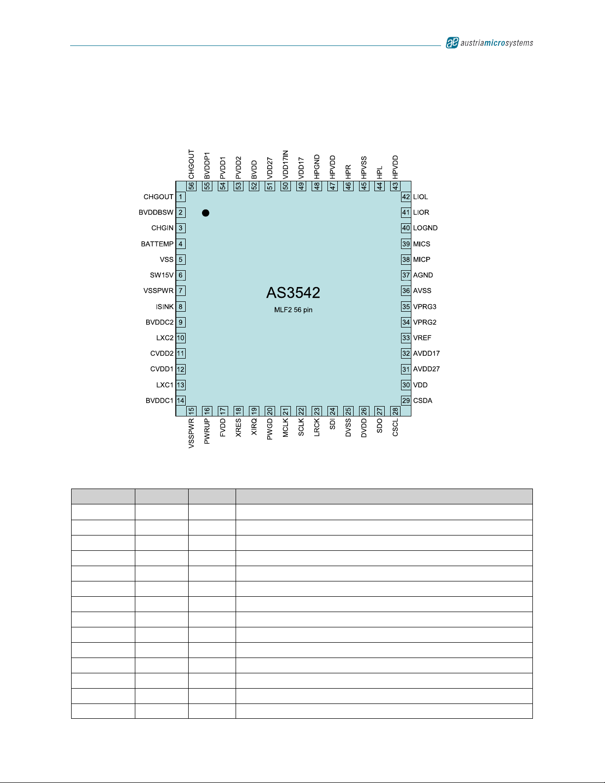
4 Pinout
4.1 Pin Assignment
Figure 2. Pin Assignments (Top View)
4.2 Pin Description
Table 2. Pin Description for AS3542
Pin Number Pin Name Type Description
1 CHGOUT SUP IO Li-Ion Charger Output
2 BVDDBSW SUP IO Battery Switch output to be connected against BVDD
3 CHGIN SUP IN Li-Ion Charger Input
4 BATTEMP ANA IO Li-Ion Charger Battery Temp. Sensor Input
5 VSS GND Power Management Neg. Reference Supply
6 SW15V DIG OUT DCDC15V Switch Output to Coil
7 VSSPWR GND Power Management Neg. Supply Terminal
8 ISINK ANA IO DCDC15V Load Current Sink Terminal
9 BVDDC2 SUP IN CVDD2 Step Down Pos. Supply Terminal
10 LXC2 DIG OUT CVDD2 Step Down Switch Output to Coil
11 CVDD2 ANA IN CVDD2 and Feedback Pin
12 CVDD1 ANA IN CVDD1 and Feedback Pin
13 LXC1 DIG OUT CVDD1 Step Down Switch Output to Coil
14 BVDDC1 SUP IN CVDD1 Step Down Pos. Supply Terminal

www.austriamicrosystems.com Revision 1.10 7 - 86
AS3542 3v2
Data Sheet, Strictly Confidential - Pinout
15 VSSPWR GND Power Management Neg. Supply Terminal
16 PWRUP DIG IN Power Up Input
17 FVDD SUP IN Digital Pos. Supply (e.g. DAC, …)
18 XRES DIG OUT Reset Output
19 XIRQ DIG OUT Interrupt Request Output
20 PWGD DIG IO PowerUp Sequence Complete Output
21 MCLK DIG IN MCLK input
22 SCLK DIG IN I2S Shift Clock Input
23 LRCK DIG IN I2S Frame Clock Input
24 SDI DIG IN I2S Data Input to DAC
25 DVSS GND Digital Circuit Neg. Supply Terminal
26 DVDD SUP IN Digital Periphery Pos. Supply
27 SDO DIG OUT I2S Data Output from ADC
28 CSCL DIG IN 2 wire SERIF Clock Input
29 CSDA DIG IO 2 wire SERIF Data I/O
30 VDD ANA IO LDO output, supply input
31 AVDD27 SUP IN Analog Pos. Supply
32 AVDD17 SUP IN Audio Pos. Supply
33 VREF ANA IO DAC Reference Pin
34 VPRG2 ANA IN Memory Supply Voltage Definition Pin
35 VPRG3 ANA IN PowerUp Sequence Definition Pin
36 AVSS GND Ground (analog)
37 AGND ANA IO Analog Common Mode Voltage Pin
38 MICP ANA IN Microphone Input
39 MICS ANA IO Microphone Supply Output / Remote Control input
40 LOGND ANA IO Line Output Common Mode Voltage Pin
41 LIOR ANA IO Analog Line Input 1 Right Channel
42 LIOL ANA IO Analog Line Input 1 Right Channel
43 HPVDD SUP IN Headphone Supply default 1.8V (max. 3.6V)
44 HPL ANA OUT Headphone Output Left Channel
45 HPVSS GND Headphone Ground
46 HPR ANA OUT Headphone Output Right Channel
47 HPVDD SUP IN Headphone Supply default 1.8V (max. 3.6V)
48 HPGND ANA IO Headphone Common Mode Voltage Pin
49 VDD17 SUP IO LDO1 Output default 1.7V
50 VDD17IN SUP IN LDO1 Pos. Supply Terminal
51 VDD27 SUP IO LDO2 Output default 2.7V
52 BVDD SUP IN Main Battery Supply Input (2.7-5.5V)
Table 2. Pin Description for AS3542
Pin Number Pin Name Type Description

www.austriamicrosystems.com Revision 1.10 8 - 86
AS3542 3v2
Data Sheet, Strictly Confidential - Pinout
53 PVDD2 ANA OUT LDO4 Output (PVDD2)
54 PVDD1 ANA OUT LDO3 Output (PVDD1)
55 BVDDP1 SUP IN LDO3 Pos. Supply Terminal
56 CHGOUT SUP IO Li-Ion Charger Output (battery switch input)
Table 2. Pin Description for AS3542
Pin Number Pin Name Type Description
www.austriamicrosystems.com Revision 1.10 9 - 86
AS3542 3v2
Data Sheet, Strictly Confidential - Absolute Maximum Ratings
5 Absolute Maximum Ratings
Stresses beyond those listed in Table 3 may cause permanent damage to the device. These are stress ratings only,
and functional operation of the device at these or any other conditions beyond those indicated in Electrical Character-
istics on page 11 is not implied. Exposure to absolute maximum rating conditions for extended periods may affect
device reliability. The device should be operated under recommended operating conditions.
Table 3. Absolute Maximum Ratings
Parameter Min Max Units Comments
5V pins -0.5 7.0 V
Applicable for pins BVDD, BVDDC1,
BVDDC2, BVDDP1, BVDDBSW,
CHGIN, CHGOUT, VBUS, CSCL,
CSDA, PWRUP
3V pins -0.5 5.0 V
Applicable for pins DVDD, HPVDD,
FVDD, VDD17IN, VDD, VPRG2,
VPRG3
15V pins -0.5 17 V Applicable for pin SW15V, ISINK
Voltage difference at VSS terminals -0.5 0.5 V Applicable for pins VSS, VSS15V,
CVSS12, HPVSS, AVSS, DVSS
3.3V pins with protection to AVDD27 -0.5 5.0
AVDD27 V Applicable for pins BATTEMP, HPGND
3.3V pins with protection to DVDD -0.5 5.0
DVDD+0.5 VApplicable for pins MCLK, LRCK, SCLK,
SDI, SDO, XIRQ, XRES, PWGD
3.3V pins with protection to AVDD17 -0.5 5.0
AVDD17+0.5 VApplicable for pins LIOL/R, LOGND,
VREF, AGND, MICP,MICS
3.3V pins with protection to HPVDD -0.5 5.0
HPVDD+0.5 V Applicable for pins HPCM, HPR/L
voltage regulator pins with protection
to BVDD -0.5 5.0
BVDD+0.5 VApplicable for pins AVDD27, PVDD1/2,
CVDD1, LXC1, CVDD2, LXC2
voltage regulator pins with protection
to AVDD17IN -0.5 5.0
AVDD17IN +0.5 V Applicable for pins AVDD17
Input Current (latch-up immunity) -100 100 mA Norm: JEDEC 17
Continuous Power Dissipation (TA= +70ºC)
Continuous power dissipation 600 mW PT1for MLF56 package
Electrostatic Discharge
Electrostatic Discharge HBM +/-1 kV Norm: JEDEC JESD22-A114C
Temperature Ranges and Storage Conditions
Operating Temperature Range -20 +85 ºC
Junction Temperature +110 ºC
Storage Temperature Range -50 +125 ºC
Humidity non-condensing 5 85 %

www.austriamicrosystems.com Revision 1.10 10 - 86
AS3542 3v2
Data Sheet, Strictly Confidential - Absolute Maximum Ratings
Bump Temperature (soldering)
Package Body Temperature 260 °C Norm IPC/JEDEC J-STD-020C, reflects
moisture sensitivity level only
Moisture Sensitive Level 3 1 Represents a max. floor live time of
168h
1. Depending on actual PCB layout and PCB used
Table 3. Absolute Maximum Ratings
Parameter Min Max Units Comments

www.austriamicrosystems.com Revision 1.10 11 - 86
AS3542 3v2
Data Sheet, Strictly Confidential - Electrical Characteristics
6 Electrical Characteristics
BVDD=+2.7V...+5.5V, TA=-20ºC...+85ºC. Typical values are at BVDD=+3.6V, TA=+25ºC, unless otherwise specified.
Table 4. Electrical Characteristics
Symbol Parameter Condition Min Typ Max Unit
Supply Voltages
BVDDx
Battery Supply Voltage
BVDD, BVDDBSW,
BVDDC1, BVDDC2,
BVDDP1
2.7 3.6 5.5 V
VBUS USB VBUS Voltage 5.0 5.5 V
CHGIN Charger Supply Voltage 4.5 5.5 V
HPVDD HP Supply Voltage 1.8 3.6 V
DVDD Digital Periphery Supply
Voltage 1.8 2.9 3.6 V
VDD17IN LDO1 Input Voltage 1.8 3.6 V
FVDD Digital Supply Voltage 1.75 1.8 2.0 V
AVDD27 Analogue Supply Voltage 2.6 2.7 3.5 V
AVDD17 Analogue Supply Voltage 1.7 1.7 3.5 V
AGND Analog Ground Voltage Internally generated AVDD17
/2 V
VDELTA-
Difference of Negative
Supplies
CVSS12, VSS15V, HPVSS,
AVSS, DVSS, VSS
To achieve good performance, the
negative supply terminals should be
connected to low impedance ground
plane.
-0.1 0.1 V
VDELTA+Difference of Positive
Supplies
RVDD-AVDD27; AVDD17-AVDD27;
FVDD-AVDD27 0V
HPVDD-AVDD27 0.3 V
AVDD27-BVDD 0.1 V
POR & Watchdog
VPOR_ON Power-on Reset Activation
Level
Power-on Reset activation level when
DVDD decreases 2.15 V
VPOR_OFF Power-on Reset Release
Level
Power-on Reset release when DVDD
increases 2.0 V
VPOR_HY Power-on Hysteresis 100 mV
fLRCLK_WD LRCLK Watchdog 2 4.1 8 kHz
PWRUP
tON_DELAY Delay Time of pin PWRUP Minimum key press time 30 ms
VPWRUP_L Input Level LOW, Pin PWRUP, BVDD>3V 0.5 V
VPWRUP_H Input Level HIGH Pin PWRUP, BVDD>3V BVDD/
3V
Pin PWRUP, BVDD<=3V 1 V
IPWRUP Internal Pull-down Current
Source Pin PWRUP; @2.9V 2.5 7 19 uA

www.austriamicrosystems.com Revision 1.10 12 - 86
AS3542 3v2
Data Sheet, Strictly Confidential - Electrical Characteristics
Digital Inputs/Outputs
VDO_DL Digital Output Driver
Capability (drive LOW)
Pins XRES, XIRQ, PWGD @ 6mA,
push/pull mode only, SDO
10%
DVDD V
VDO_DH Digital Output Driver
Capability (drive HIGH)
Pins XRES, XIRQ PWGD @ 6mA,
push/pull mode only, SDO
90%
DVDD V
IPU Internal Pull-up Current
Source Pins XRES, XIRQ, PWGD; @ 0V 10 µA
VDI_L Digital Input Level LOW Pin SDI, SCLK, MCLK, LRCK 30%
DVDD V
VDI_H Digital Input Level HIGH Pin SDI, SCLK, MCLK, LRCK 70%
DVDD V
fCLK Audio Clock Frequency LRCK according to streamed audio
data 848kHz
Power Requirements
IREF Reference supply current all regulators off, only LDO2 on 210 uA
IBIAS Audio Bias current 32 uA
ISUM Summing stage current 174 uA
ILIN Line input stage current no signal 146 uA
IMIC Mic input stage current no signal 643 uA
IMICS Mic Supply stage current no load 201 uA
ILOUT Line output stage current no load 436 uA
IDAC_GS DAC gain stage current no signal 214 uA
IADC_GS ADC gain stage current no signal 1,36 mA
IHPH Headphone stage current
1.8V, no load 0,95
mA
1.8V, Bias on, no load 1,21
1.8V, CM buffer on, no load 1,37
1.8V, Bias on, CM buffer on, no load 1,77
1.8V, HQ on 1,24
IDAC DAC supply current
LRCK=48kHz 1,48
mA
LRCK=44.1kHz 1,41
LRCK=32kHz 1,19
LRCK=16kHz 0,91
LRCK=8kHz 0,76
IADC ADC supply current
LRCK=24kHz 1,7
mA
LRCK=22.05kHz 1,69
LRCK=16kHz 1,64
LRCK=8kHz 1,58
LRCK=4kHz 1,55
IRTC RTC supply current 600 nA
Table 4. Electrical Characteristics (Continued)
Symbol Parameter Condition Min Typ Max Unit
www.austriamicrosystems.com Revision 1.10 13 - 86
AS3542 3v2
Data Sheet, Strictly Confidential - Electrical Characteristics
6.1 Audio Specification
BVDD=+3.6V, VDD27=+2.7V, HPVDD=FVDD=1.8V, VDD17=+1.7V, fS=48kHz, TA=+25ºC, unless otherwise specified.
Table 5. Electrical Characteristics
Symbol Parameter Condition Min Typ Max Unit
DAC Input to Line Output
FS Full Scale Output RL= 10kΩ, f=1kHz, 1VRMS input 0,568 VRMS
SNR Signal to Noise Ratio A-weighted, no load, silence input 96 dB
DR Dynamic Range A-weighted, no load, -60dB FS, f=1kHz 95 dB
THD Total Harmonic Distortion 1kHz -1dB FS input, RL=10kΩ-90 dB
CS Channel Separation RL=10kΩ62 dB
Line Input to Line Output
FS Full Scale Output RL= 10kΩ, f=1kHz, 545mVRMS input 0,545 VRMS
SNR Signal to Noise Ratio A-weighted, no load, silence input 97 dB
THD Total Harmonic Distortion 1kHz 1VRMS (-1dB FS) input, RL=10kΩ-81 dB
CS Channel Separation RL=10kΩ100 dB
DAC Input to HP Output
FS Full Scale Output RL=32Ω0,560 VRMS
RL=16Ω0,550 VRMS
SNR Signal to Noise Ratio A-weighted, no load, silence input 97 dB
DR Dynamic Range A-weighted, no load, -60dB FS, f=1kHz 94 dB
THD Total Harmonic Distortion
no load, f=1kHz, FS input -87 dB
POUT=6mW, RL=32Ω, f=1kHz, -1dB FS -81 dB
POUT=12mW, RL=16Ω, f=1kHz, -1dB FS -78 -60 dB
CS Channel Separation RL=32Ω63 dB
RL= 16Ω60 dB
Line Input to HP Output
FS Full Scale Output RL= 32Ω, f=1kHz, 545mVRMS(FS) input 0,450 VRMS
RL= 16Ω, f=1kHz, 545mVRMS(FS) input 0,447 VRMS
SNR Signal to Noise Ratio A-weighted, no load, silence input 97 dB
THD Total Harmonic Distortion
no load, f=1kHz, 545mVRMS -77 dB
POUT=6mW, RL=32Ω, f=1kHz, 545mVRMS -75 dB
POUT=12mW, RL=16Ω, f=1kHz, 545mVRMS -75 -60 dB
CS Channel Separation RL= 32Ω77 dB
RL= 16Ω66 dB
Mic Input to Line Output
FS Full Scale Output f=1kHz, 27mVRMS FS input 0,512 VRMS
SNR Signal to Noise Ratio A-weighted, no load, silence input 75 dB
THD Total Harmonic Distortion 1kHz 27mVRMS FS input 77 dB
Mic Input to ADC Output
SNR Signal to Noise Ratio A-weighted, no load, silence input 80 dB
DR Dynamic Range A-weighted, no load, -60dB FS, f=1kHz 77 dB
THD Total Harmonic Distortion 1kHz 27mVVRMS FS input -64 dB

www.austriamicrosystems.com Revision 1.10 14 - 86
AS3542 3v2
Data Sheet, Strictly Confidential - Typical Operating Characteristics
7 Typical Operating Characteristics
BVDD = +3.6V, TA= +25ºC, unless otherwise specified.
www.austriamicrosystems.com Revision 1.10 15 - 86
AS3542 3v2
Data Sheet, Strictly Confidential - Detailed Description - Audio Functions
8 Detailed Description - Audio Functions
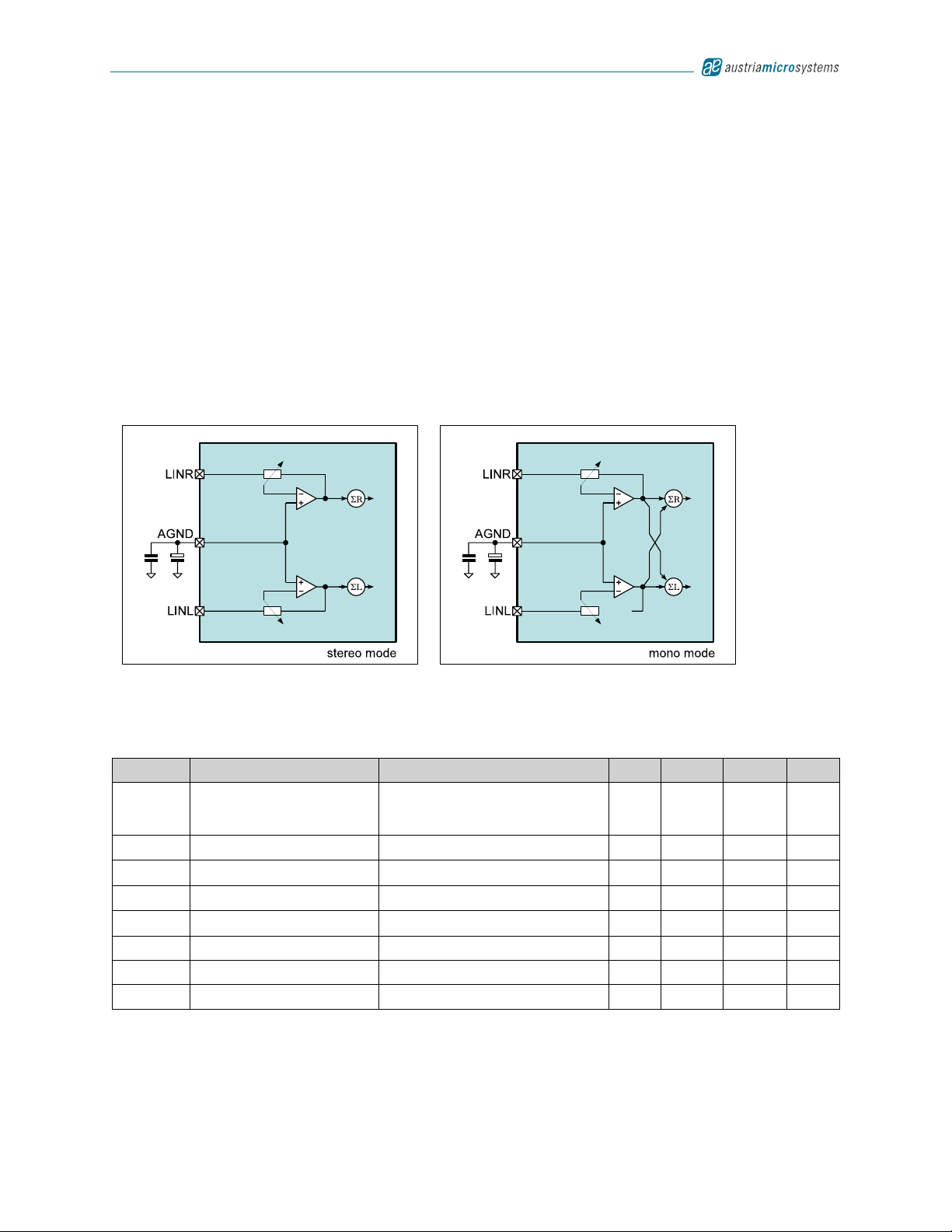
8.1 Audio Line Input
8.1.1 General
The chip features two identical line inputs. The blocks can work in 2x mono single ended or in stereo single ended
mode.
The volume control has an independent gain regulation for left and right channel with 32 steps @ 1.5dB each and
MUTE. The gain can be set from –40.5dB to +6dB. The stage is set to mute by default. If the line input is not enabled,
the volume settings are set to their default values. Changing the volume and mute control can only be done after
enabling the input.
Line Input and Line Output are sharing the same pins. Please make sure to disable the line out discharge resistors
when using line input (LO_DISCHG_OFF in reg. 0Bh).
Figure 3. Line Inputs
8.1.2 Parameter
AVDD17=1.7V, AVDD27=2.7V, TA= 25oC, unless otherwise mentioned
Table 6. Line Input Parameter
Symbol Parameter Condition Min Typ Max Unit
VLIN Input Signal Level
Pls observe gain settings. Max.
peak levels at any node within the
circuit shall not exceed AVDD
AVDD17
/3
AVDD17
/2 VPEAK
RLIN Input Impedance depending on gain setting 8-25 kΩ
ΔRLIN Input Impedance Tolerance ±30 %
CLIN Input Capacitance 5 pF
ALIN Programmable Gain -40.5 +6 dB
Gain Steps discrete logarithmic gain steps 1.5 dB
Gain Step Accuracy ±0.25 dB
ALINMUTE Mute Attenuation 100 dB
www.austriamicrosystems.com Revision 1.10 16 - 86
AS3542 3v2
Data Sheet, Strictly Confidential - Detailed Description - Audio Functions
8.1.3 Register Description
Line input has to be enabled in register 14h first before other settings in register 0Ah and 0Bh can be programmed.
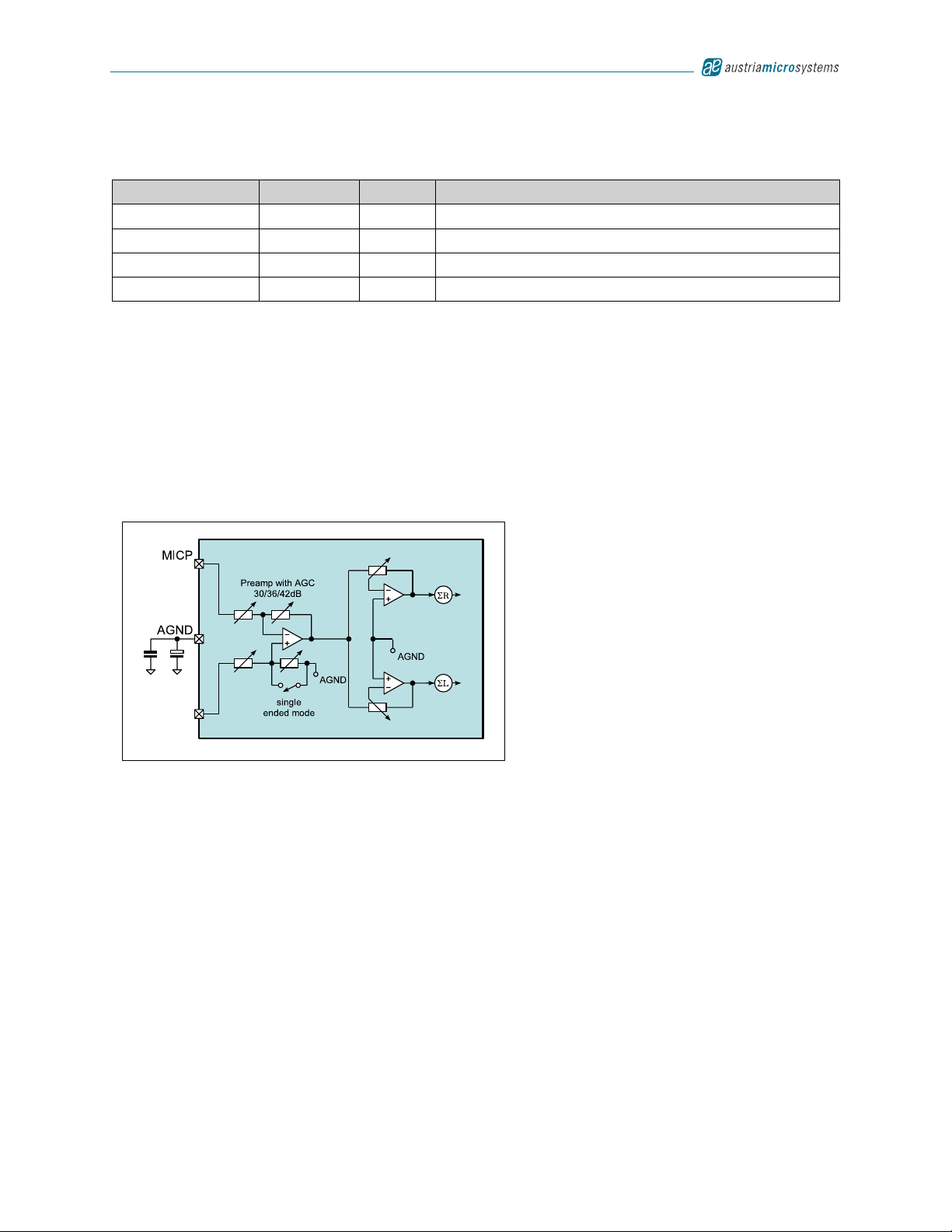
8.2 Microphone Input
8.2.1 General
The AFE offers one microphone input and one low noise microphone voltage supply (microphone bias), voice activa-
tion, microphone connect detection and push button remote control.
Please not that only single ended mode is possible for the microphone input, make sure that the MIC_MODE in reg.
06h is set for enalbing the single ended mode.
Figure 4. Microphone Input
8.2.2 Gain Stage & Limiter
The integrated pre-amplifier allows 3 preset gain settings. There is also a limiter which attenuates high input signals
from e.g. electret microphones signal to 1Vp. The AGC has 128 steps with 0.375dB with a dynamic range of the full
pre-amplifier level. The AGC is ON by default but can be disabled by a microphone register bit.
Apart from the microphone pre-amplifier the microphone input signal can further be amplified with 32 @1.5dB pro-
grammable logarithmic gain steps and MUTE. All gains and MUTE are independently programmable. The gain can be
set from –40.5dB to +6dB.
The stage features a soft-start function. Pre-amplifier and gain-stage settings can be set before enabling the micro-
phone stage. After enabling the stage to gain is automatically set to the defined value by using the 128 steps of the
AGC.
8.2.3 Supply & Detection
Each microphone input generates a supply voltage of 1.5V above HPCM. The supply is designed for ≤2mA and has a
6.5mA current limit. In OFF mode the MICS terminal is pulled to AVDD with 20kOhm. A current of typically 50uA gen-
erates an interrupt to inform the CPU, that a circuit is connected. When using HPCM as headset ground the HP–stage
gives the interrupt. After enabling the HP-stage through the CPU the microphone detection interrupt will follow.
When using the MICS terminal as ADC-10 input to monitor external voltages the 20kOhm pull-up has to be disabled by
disabling the interrupt for microphone detection.
Table 7. Line Input Related Register
Name Base Offset Description
LINE_IN_R 2-wire serial 0Ah Right Line Input settings
LINE_IN_L 2-wire serial 0Bh Left Line Input settings
AudioSet1 2-wire serial 14h Enable/disable driver stage
AudioSet3 2-wire serial 16h Enable/disable mixer input

www.austriamicrosystems.com Revision 1.10 17 - 86
AS3542 3v2
Data Sheet, Strictly Confidential - Detailed Description - Audio Functions
8.2.4 Remote Control
Fast changes of the supply current of typically 500uA are detected as a remote button press, and an interrupt is gener-
ated. Then the CPU can start the measurement of the microphone supply current with the internal 10-bit ADC to distin-
guish which button was pressed. As the current measurement is done via an internal resistor, only two buttons
generating a current of about 0.5mA and 1mA can be detected. With this, 1mA as microphone bias is still available.
8.2.5 Voice Activation
Further a built-in voice activation comparator can actuate an interrupt if microphone input voltage of about 5mVRMS is
detected.
8.2.6 Parameter
AVDD17=1.7V, AVDD27=2.7V, TA= 25oC unless otherwise mentioned
Table 8. Microphone Input Parameter
Symbol Parameter Condition Min Typ Max Unit
VMICIN0Input Signal Level AMICPRE = 30dB; AMIC = 0dB 20 mVP
VMICIN1A
MICPRE = 36dB; AMIC = 0dB 10 mVP
VMICIN2A
MICPRE = 42dB; AMIC = 0dB 5mVP
RMICIN Input Impedance MICP to AGND 7.5 kΩ
ΔMICIN Input Impedance Tolerance -7
+33 %
CMICIN Input Capacitance 5 pF
AMICPRE Microphone Preamplifier
Gain
Preamplifier has 3 selectable (fixed)
gain settings
30
36
42
dB
AMIC Programmable Gain -40.5 +6 dB
Gain Steps discrete logarithmic gain steps 1.5 dB
Gain Step Precision ±0.25 dB
VATTACK Limiter Activation Level 0.57 VPEAK
VDECAY Limiter Release Level 0.47 VPEAK
AMICLIMIT Limiter Gain Overdrive 128 @ 0.375dB
30
36
42
dB
tATTACK Limiter Attack Time 50 µs/6dB
tDECAY Limiter Decay Time 120 ms/
6dB
AMICMUTE Mute Attenuation 100 dB
VMICSUP Microphone Supply Voltage depending on V_MICS setting
2
1.55
1.26
1.06
V
IMICMAX Max. Microphone Supply
Current
microphones nominally need a bias
current of 0.5mA-1mA 6.5 mA
VNOISE Microphone Supply Voltage
Noise 5µV
IMICDET Microphone Detection
Current 50 µA
IREMDET Max. Remote Detection
Current 500 µA
www.austriamicrosystems.com Revision 1.10 18 - 86
AS3542 3v2
Data Sheet, Strictly Confidential - Detailed Description - Audio Functions
8.2.7 Register Description
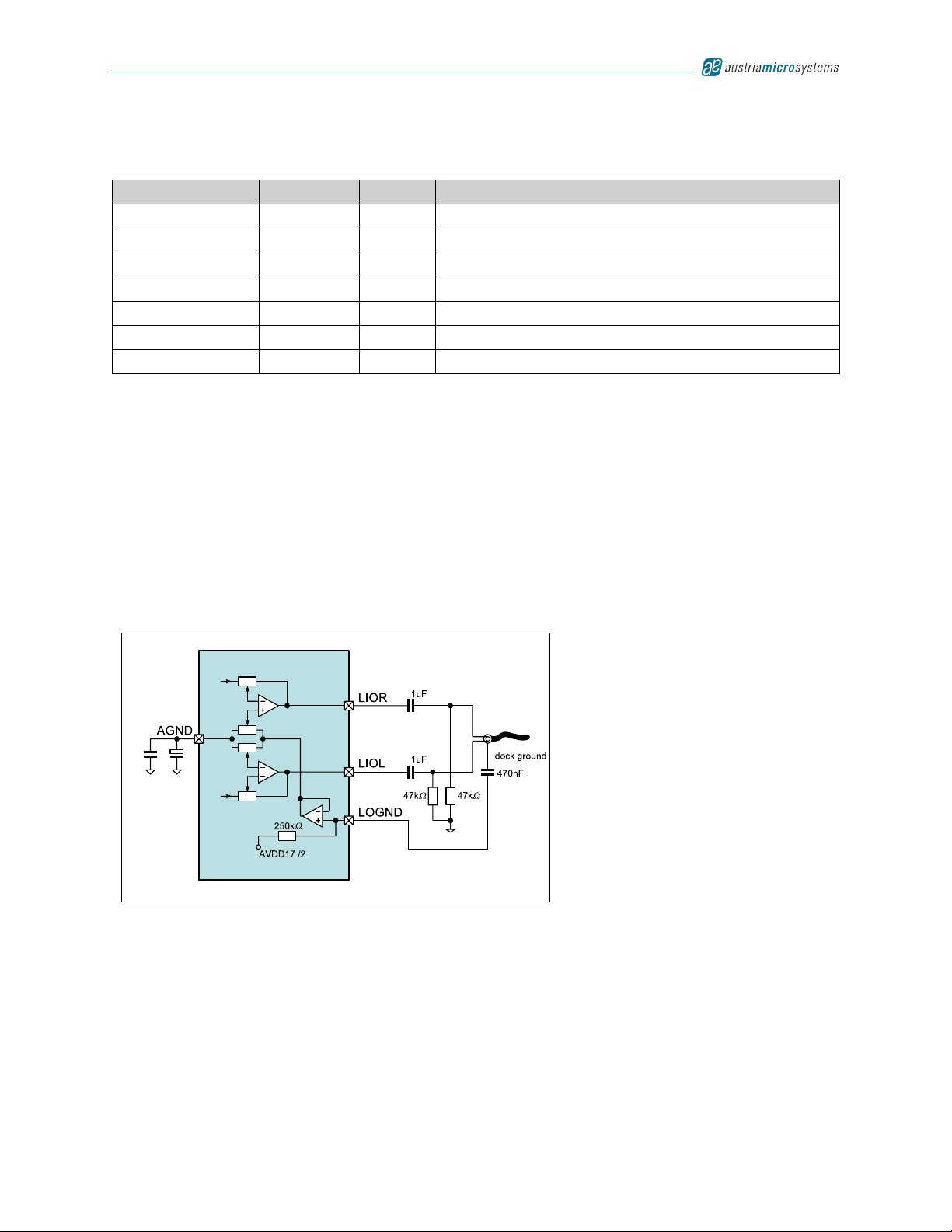
8.3 Line Output
8.3.1 General
The line output is designed to provide the audio signal with a typical VPEAK level at a load of minimum 10kΩ, which is a
minimum value for line inputs. If the limiters (N20/N21) are deactivated the peak output voltage is AVDD17/2 Vp.
This AFE has a combined output stage for headphone and line output with an independent gain regulation for left and
right channel with 32 steps @ 1.5dB each. The gain can be set from -40.5dB to +6dB.
If the line output is not enabled, the volume settings are set to their default values. Changing of volume and mute con-
trol can only be done after enabling the output.
Line Output and Line Input are sharing the same pins.
Figure 5. Line Output
8.3.2 Auto Fading
By setting a new output volume level, the stage does a automatic fading from the current gain setting to the new target.
Changing the input multiplexer from one source to another will be done by fadeing out to mute, source changing and
fading in of the new source to the target volume. Change from HPH-out to LINE-out is done by fading out of HPH-out
to mute and fading in of the LINE-out to the target volume.
The fading speed can be programmed to 3 different speed levels. The immediate response can be selected as 4th
state.
8.3.3 Ground Noise Cancelation
A separate ground input allows to connect a ground sense line direct from the dock connector ground or line out jack
shield to make the audio output independent from PCB ground noise.
Table 9. Microphone Input Related Register
Name Base Offset Description
MIC_R 2-wire serial 06h Right Microphone Input volume settings, AGC control
MIC_L 2-wire serial 07h Left Microphone Input volume settings, MIC supply control
AudioSet1 2-wire serial 14h Enable/disable driver stage
AudioSet3 2-wire serial 16h Enable/disable mixer input
IRQENRD_1 2-wire serial 24h Interrupt settings for microphone voice activation
IRQENRD_3 2-wire serial 26h Interrupt settings for microphone detection
IRQENRD_4 2-wire serial 27h Interrupt settings for remote button press detection

www.austriamicrosystems.com Revision 1.10 19 - 86
AS3542 3v2
Data Sheet, Strictly Confidential - Detailed Description - Audio Functions
8.3.4 Parameter
AVDD17=1.7, AVDD27=2.7, TA= 25oC, unless otherwise mentioned
8.3.5 Register Description
8.4 Headphone Output
The headphone output is designed to provide the audio signal with 2x40mW @ 16Ωor 2x20mW @32Ω, which are typ-
ical values for headphones.
This AFE has a combined output stage for headphone and line output with an independent gain regulation for left and
right channel with 32 steps @ 1.5dB each. The gain can be set from -40.5dB to +6dB.
Figure 6. Headphone Output
Table 10. Line Output Parameter
Symbol Parameter Condition Min Typ Max Unit
RL_LO Load Impedance
(Stereo Mode) line inputs nominally have 10kΩ5kΩ
CL_LO Load Capacitance
(Stereo Mode) 100 pF
ALO Programmable Gain -40.5 +6 dB
Gain Steps discrete logarithmic gain steps 1.5 dB
Gain Step Accuracy ±0.25 dB
ALOMUTE Mute Attenuation 100 dB
Table 11. Line Output Related Register
Name Base Offset Description
OUT_R 2-wire serial 00h Right Line Output volume settings, MUX control
OUT_L 2-wire serial 01h Left Line Output volume settings
AudioSet2 2-wire serial 15h Auto fading timing settings
AudioSet3 2-wire serial 16h Enable/disable mixer input

www.austriamicrosystems.com Revision 1.10 20 - 86
AS3542 3v2
Data Sheet, Strictly Confidential - Detailed Description - Audio Functions
8.4.1 Phantom Ground
There are 2 ways to connect a headphone to the AFE. In order to spare the bulky ac/dc de-coupling capacitors at pins
HPR/HPL a buffered ground (Phantom Ground) is provided. This Common Mode Buffer needs to be switched on if
utilized. If form factor considerations are less stringent, the headphones can be conventionally connected via 2x200µF
capacitors.
Figure 7. Headphone Output using Common Mode Buffer
8.4.2 No-Pop Function
The output is automatically set to mute when the output stage is disabled.
To avoid Pop-Click noise during power-up and shut-down of the headphone amplifier, a charge/discharge control of
HPGND (0V-HPVDD/2-0V) at pins HPR/HPL is incorporated into the AFE. The 470nF capacitor at pin HPGND is used
to form the charge/discharge slope. Pls observe that pin HPGND is a high impedance node which must not be
connected to any other external device than the 470nF buffer capacitor. To avoid Pop-Click noise one has to wait for
750ms in between a power-down (switch-off) and a power-up (switch-on) of the headphone amplifier.
8.4.3 Auto Fading
By setting a new output volume level, the stage does a automatic fading from the current gain setting to the new target.
Changing the input multiplexer from one source to another will be done by fading out to mute, source changing and
fading in of the new source to the target volume. Change from HPH-out to LINE-out is done by fading out of HPH-out
to mute and fading in of the LINE-out to the target volume.
The fading speed can be programmed to 3 different speed levels. The immediate response can be selected as 4th
state.
Figure 8. Headphone Startup with MaxGain Settings
This manual suits for next models
1
Table of contents


