Auvidea JNX42 Product manual

AUVIDEA
JNX42
TECHNICAL
REFERENCE
MANUAL
SCOPE OF WORK
Providing technical information and documentation to the product line JNX42 for Nvidia
Jetson Orin Nano & Orin NX
PCB NUMBER
38556
ISSUE DATE [REVISED DATE]
May.2023 [25.MAY.2023]
Version
1.4
PAGES
31

JNX42 TECHNICAL REFERENCE MANUAL
VERSION: 1.0 Page 2 of 31 Apr 2023
Contents
SECTION 1 Document revisions and changes ................................................................ 4
SECTION 2 Product revisions and changes .................................................................... 5
SECTION 3 Overview .................................................................................................... 6
3.1 JNX42 ........................................................................................................................................................... 6
3.2 JNX42 features and comparison .................................................................................................................. 6
3.3 Technical specifications ............................................................................................................................... 7
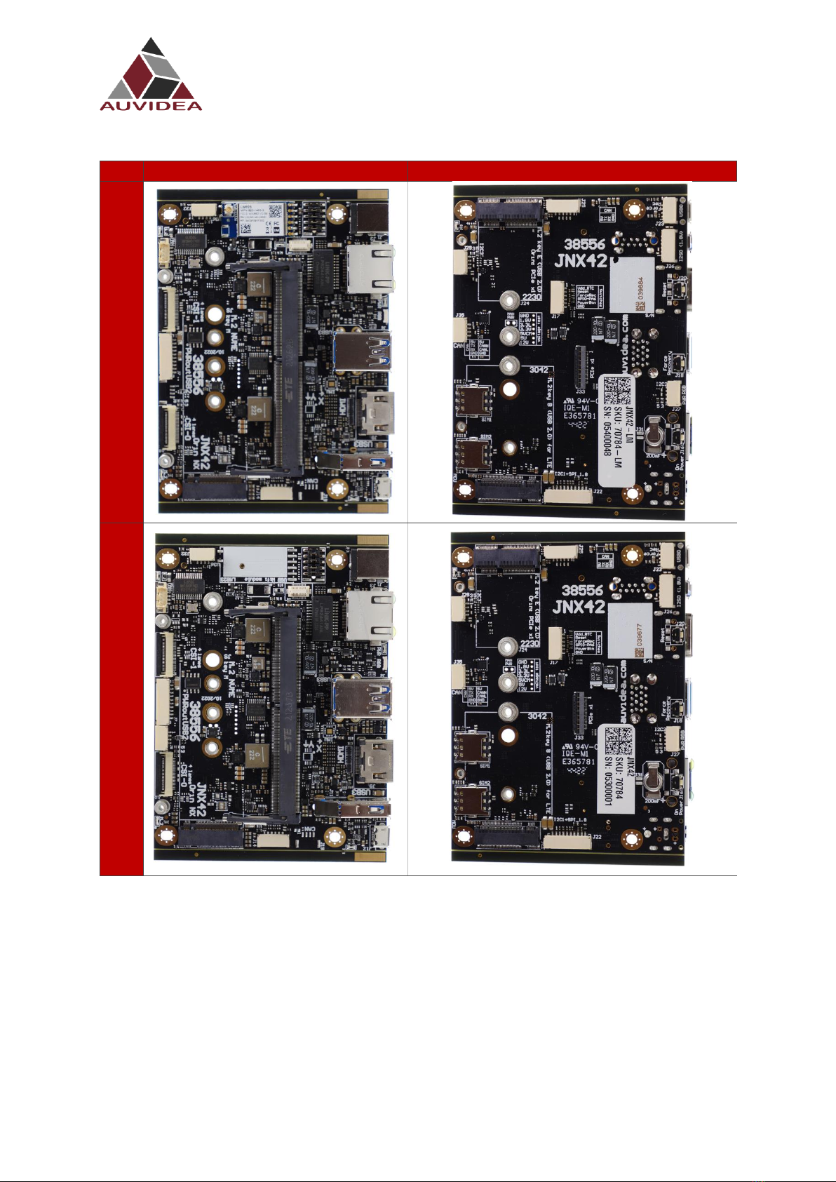
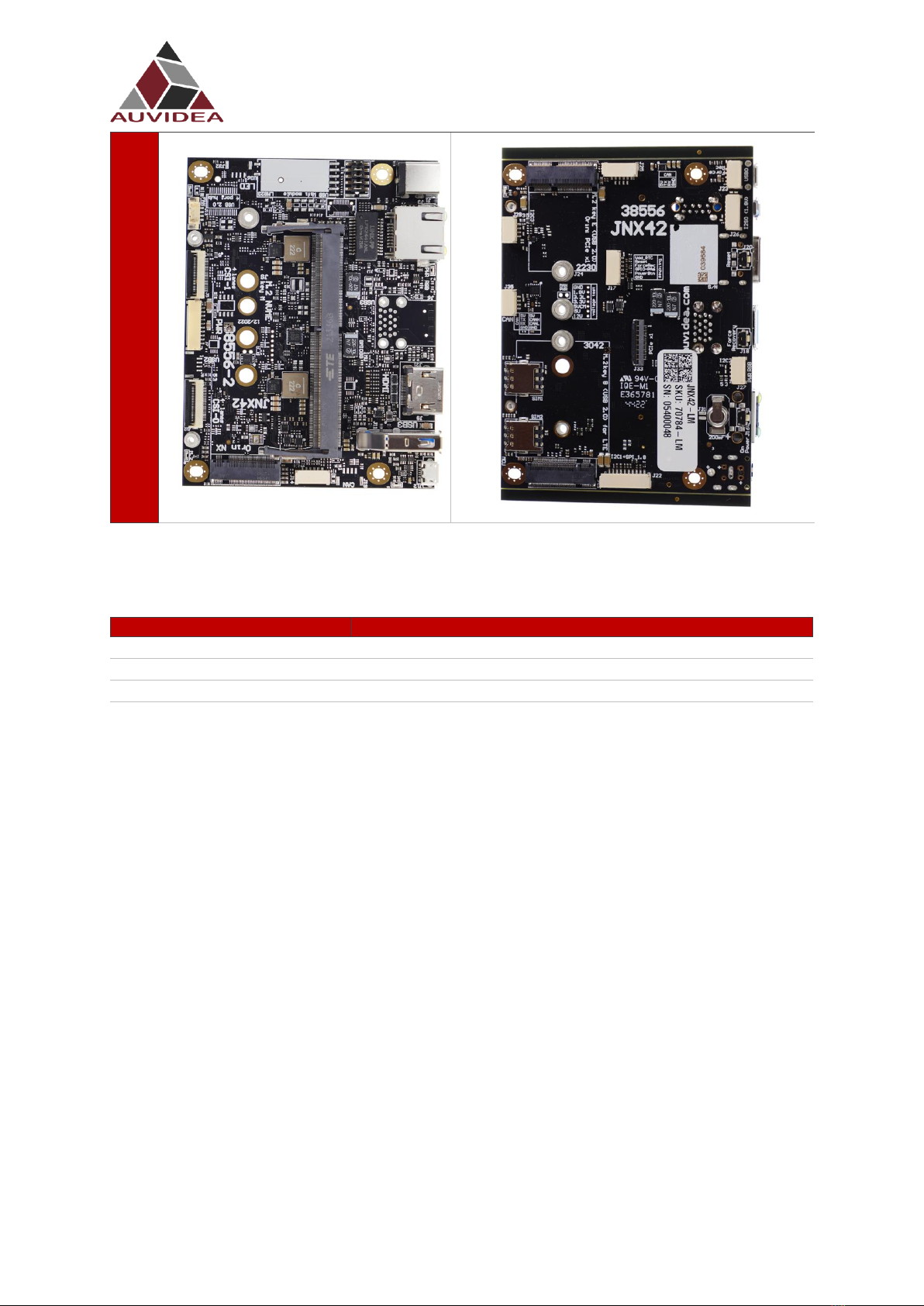
3.4 Model pictures............................................................................................................................................. 8
3.5 Power consumption..................................................................................................................................... 9
3.6 Options ........................................................................................................................................................ 9
SECTION 4 FEATURES ..................................................................................................10
4.1 Crypto chip (optional)................................................................................................................................ 10
4.2 MCU chip ................................................................................................................................................... 10
SECTION 5 Pinout description top side.........................................................................11
5.1 J1 - Power input jack.................................................................................................................................. 11
5.2 J3 - Ethernet (GbE)..................................................................................................................................... 11
5.3 J4 - M.2 PCIEx4 NVME SSDs ....................................................................................................................... 12
5.4 J5 - CSI-2 CD ............................................................................................................................................... 12
5.5 J6 USB 3.0 –3.1.......................................................................................................................................... 13
5.6 J7 –Power out ........................................................................................................................................... 14
5.7 J8 - USB 2.0 ................................................................................................................................................ 14
5.8 J9 - HDMI.................................................................................................................................................... 14
5.9 J10 - CSI-2 AB ............................................................................................................................................. 14
5.10 J11 - USB 3.0 –3.1...................................................................................................................................... 14
5.11 J12 - Micro USB.......................................................................................................................................... 15
5.12 J14 –UART Connector ............................................................................................................................... 15
5.12.1 UART configuration of the JNX42 ...................................................................................................... 16
5.13 J19 –CAN ................................................................................................................................................... 16
5.14 J+20 - Reset Button.................................................................................................................................... 16
5.15 J22 –SPI ..................................................................................................................................................... 17
5.16 J32 –CAM LED ........................................................................................................................................... 17
5.17 J35 CAN...................................................................................................................................................... 18
5.18 J13 - Fan connector.................................................................................................................................... 18
5.19 PoE and Power module connector ........................................................................................................... 19
5.20 U10 –IMU BMI088 .................................................................................................................................... 20
5.21 LED - PWR .................................................................................................................................................. 20
SECTION 6 Pinout description bottom side ..................................................................20
6.1 LED - Eth..................................................................................................................................................... 20
6.2 LED - Over current ..................................................................................................................................... 20
SECTION 7 FAQ ...........................................................................................................21

JNX42 TECHNICAL REFERENCE MANUAL
VERSION: 1.0 Page 3 of 31 Apr 2023
SECTION 8 Disclaimer..................................................................................................22
SECTION 9 Copyright notice.........................................................................................23
SECTION 10 Appendix A [CSI-Cameras]..........................................................................24
10.1 Camera connection example ..................................................................................................................... 24
SECTION 11 Appendix B [GPIO] .....................................................................................25
11.1 GPIO control .............................................................................................................................................. 25
11.1.1 Change direction to in ....................................................................................................................... 25
11.1.2 Change direction to out..................................................................................................................... 25
11.1.3 Set GPIO low ...................................................................................................................................... 25
11.1.4 Set GPIO high..................................................................................................................................... 25
11.1.5 Readout GPIO value........................................................................................................................... 25
11.2 Pin to GPIO reference sheet for Xavier-NX/Nano/TX2-NX ........................................................................ 26
11.3 How to calculate GPIOs.............................................................................................................................. 27
11.3.1 GPIOnumber ...................................................................................................................................... 27
11.3.2 GPIOletter.......................................................................................................................................... 27
11.3.3 GPIOnumber ...................................................................................................................................... 27
11.3.4 GPIOoffset ......................................................................................................................................... 27
11.3.5 Example ............................................................................................................................................. 27
11.3.6 Table.................................................................................................................................................. 28
SECTION 12 Appendix C [I2C] ........................................................................................29
12.1 I2C device bus ............................................................................................................................................ 29
12.2 I2C usage of devices and registers............................................................................................................. 29
12.2.1 List i2c devices on a specific bus ........................................................................................................ 29
12.2.2 Dump i2c device registers.................................................................................................................. 30
12.2.3 Set register value:.............................................................................................................................. 30
12.2.4 Read register value:........................................................................................................................... 30
12.2.5 Test IMX219 camera stream ............................................................................................................. 30
SECTION 13 END OF DOKUMENT...................................................................................31

JNX42 TECHNICAL REFERENCE MANUAL
VERSION: 1.0 Page 4 of 31 Apr 2023
SECTION 1 Document revisions and changes
Document
version
Changes
V1.0
Initial document, internal verification process
V1.1
internal verification process

JNX42 TECHNICAL REFERENCE MANUAL
VERSION: 1.0 Page 5 of 31 Apr 2023
SECTION 2 Product revisions and changes
Product
version
Changes
38556
▪First version
38556-2
▪swapped CAM1_PWR and CAM2_PWR ( rev 1 needs device tree change, to
correct this in software) –rev 2 is now compatible to the NVIDIA device tree
▪RXD pulldown added
▪added coin cell holder for 6.8mm cells (MC621, V364, SC621, MS518SE,
MS621FE) –optional
▪added EEPROM
▪changed IMU to BMI088
▪added Harting 3 pin power input connector (Harting 14110313002000):
1 - 24V AO
2 - 24V (GPIO)
3 –GND
connect ignition controlled power to pin 2 (J37)
▪added J30 coin cell holder for 10mm cells (CR1025) –optional
▪added J18 coin cell holder for 20mm cells (CR2032) –default configuration
▪added JST-SM alternative to RJ45 - optional
38556-3
(planned)
▪Change UART routing to connector (add console UART)

JNX42 TECHNICAL REFERENCE MANUAL
VERSION: 1.0 Page 6 of 31 Apr 2023
SECTION 3 Overview
3.1 JNX42
The JNX42 carrier board has been designed for the Jetson Orin Nano and Orin NX primarily.
(Nano, TX2NX and Xavier NX will only support one USB 3.0 port and only one CSI-2 interface.)
The JNX42 supports low level remote system management features:
▪remote power cycle
▪change of boot device
Orin: primary: SSD, secondary: USB
Nano/TX2NX/Xavier NX: primary eMMC, secondary: SSD or vice versa)
▪Limited remote debugging
Please note that the JNX44/45/46 offer enhanced system management features.
The features above are implemented with the following hardware:
▪UART connection between MCU and LTE module
this requires a LTE module with USB and UART (e.g. SIMCOM 7600)
it also requires firmware enhancement of the MCU
▪Console UART connection (Jetson and MCU)
Easy integration into passively cooled systems
▪Easy flashing: just connect a USB OTG cable (Auto Flash)
▪High performance storage: M.2 NVME PCIe x4
3.2 JNX42 features and comparison
Description
JNX42-LC
JNX42-LM
JNX42-M2
Power
6V - 19V (barrel
connector)
6V - 19V (barrel
connector)
6V - 19V (barrel
connector)
NX powering
5V 8A power supply
5V 8A power
supply
5V 8A power supply
DP
no
HDMI
yes
Fan
connector
Yes
M.2 NVME
Key M
yes
Micro-SD
card
no
M.2 Key E
no
yes (PCIe)
yes (USB + PCIe)
CAN RX / TX
1x (requires external transceiver)
USB 3.x
1x USB 3.1
(native - full performance)
micro USB
1x Micro USB
1x Micro USB
1x Micro USB

JNX42 TECHNICAL REFERENCE MANUAL
VERSION: 1.0 Page 7 of 31 Apr 2023
(device mode)
(host and device
mode)
(host and device
mode)
Auto Flashing
yes
(plug in host cable and flash)
USB 2.0
No
1x USB 2.0 (JST-GH, J8, J23)
Ethernet
Gigabit RJ45 (one LED)
PoE option
yes, add-on module is required
CSI
2x CSI-2 (4 lanes) plus camera LED
(hardware sync available)
UART
1x (UART2)
2x (UART 0+2)
I2C
(CSI-2 only)
3x
3x
I2S
-
1x (1.8V)
SPI
-
1x (1.8V)
Host mode: peripheral devices like mouse and keyboard may be connected
Device mode: the USB port is in “slave” mode to support connection to host PC (e.g. flashing or
remote access –virtual network connection - 192.168.55.1)
UART0: user UART port with RTS and CTS (1.8V level)
UART2: console UART port (only available with rev 3)
3.3 Technical specifications
Description
Note
HDMI
standard HDMI connector (2.0)
USB 3.1
10Gb/s
Physical size
80x 104.6mm
Mounting holes
4x 3.2mm (for M3)
Temperature range
0 to 70°C (extended range optional)
Humidity
noncondensing
Longevity
no temperature sensitive components
(like electrolytic capacitors)

JNX42 TECHNICAL REFERENCE MANUAL
VERSION: 1.0 Page 8 of 31 Apr 2023
3.4 Model pictures
Top side
Bottom side
JNX4
2-LM
JNX4
2-M2

JNX42 TECHNICAL REFERENCE MANUAL
VERSION: 1.0 Page 9 of 31 Apr 2023
3.5 Power consumption
Description
JNX42
Carrier board logic
< 1 watt
3.3/5V power converter efficiency
> 90%
Power in converter efficiency
> 90%
3.6 Differentiating features
▪Flexible design and manufacturing
▪designed and manufactured in Germany
▪in-house fully automated production line with 3D AOI
▪special configuration possible with minimum purchase of 25 pcs (display port, M.2, PoE, 48V
power in, super cap option, 2 RPi camera module connectors, SPI, I2C, switches and more.)
▪design services: you architect your custom carrier board and Auvidea designs and produces it
- please ask for a quote

JNX42 TECHNICAL REFERENCE MANUAL
VERSION: 1.0 Page 10 of 31 Apr 2023
SECTION 4 FEATURES
4.1 Crypto chip (optional)
The crypto chip is optional. Please check the data sheet of the manufacturer for details.
Model: ATSHA204A-MAHDA-T
https://ww1.microchip.com/downloads/en/DeviceDoc/ATSHA204A-Data-Sheet-40002025A.pdf
4.2 MCU chip
A on board MCU for watchdog and low level system management functions (via LTE). The MCU can receive text
messages via an UART connection to compatible LTE M.2 cards (e.g. Simcom SIM7600). With these messages
low level system management can be performed. Please note that this requires an optional MCU firmware.
The source code to this firmware may be licensed.
▪power cycle or reset
▪change of boot order
4.3 USB 2.0 hub
The LM and M2 versions feature a 4 port USB 2.0 hub controller (GL850G).
Uplink: USB1 (115/117) of the Jetson
Port 1: USB 2.0 of dual USB 3 connector (lower port)
Port 2: USB 2.0 of dual USB 3 connector (upper port)
Port 3: M.2 key B LTE slot
Port 4: LM module (LM) or M.2 key E slot (M2) plus J8 (shared)

JNX42 TECHNICAL REFERENCE MANUAL
VERSION: 1.0 Page 11 of 31 Apr 2023
SECTION 5 Pinout description top side
Please note that the software GPIO number differs from the socket pin number. This software GPIO
number must be computed with a special formula and differs between the various compute
modules. Please see appendix B for details.
5.1 J1 - Power input jack
5.5/2.5mm barrel jack
Pin
Description
Note
1
12V
12V nominal (absolute max. 20V)
recommend power supply 12V 36W (or higher)
extra features: populate optional power module
2
GND
If no power module is plugged in the supply voltage must be bridged by inserting 5 or 6 2mm
jumpers. If no jumpers are plugged then power is not applied.
Optionally the J34 Molex power connector (436500216) may be populated. Optionally power may be
supplied via J7 (2 pins)
J34: Molex power connector (optional –J1 must not be populated)
5.2 J37 - Harting power connector (LM and M2 versions)
Harting: 3 pin power input connector (Harting 14110313002000):
Pin
Description
Note
1
12V
input power (always on)
2
12V
ignition power (Jetson: pin 228 –inverted, MCU: PB4) –weak pullup
to 3.3V
3
GND
To implement ignition controlled powering the MCU firmware must be enhanced. MCU firmware
support is planned. If this pin is left open /floating) the internal pullup will iniate a power up (auto
start). Connect to GND to disable auto start and to manually power up the system.
-MCU should monitor the pin to turn on power to the Jetson
-The Jetson should monitor this pin to gracefully turn off the system
5.3 J3 - Ethernet (GbE)
Standard RJ45 pinout with PoE capable magnetics class 3 and 4 (PD or PSE). Connected to the
Ethernet controller on the compute module. PoE power is routed to the optional power module.

JNX42 TECHNICAL REFERENCE MANUAL
VERSION: 1.0 Page 12 of 31 Apr 2023
5.4 J4 - M.2 PCIEx4 NVME SSDs
Please note that only NVME SSDs are supported. SATA SSDs are not supported. We recommend the
128GB Transcend SSDs (TS128GMTE110S). This SSD is standard in some Auvidea embedded systems.
5.5 J5 - CSI-2 CD
22 pin 0.5mm pitch FPC connector (contacts down)
Pin
Description
Socket pin
Note
1
3.3V
Power: connected with bead to 3.3V
(5V optional if bead is moved)
2
SDA
215
CAM-I2C via multiplexer (3.3V)
3
SCL
213
CAM-I2C via multiplexer (3.3V)
4
GND
5
MCLK
IN: wired’OR to control CAM_LED
6
CAM1_PWDN
120
OUT: LC (1.8V), LM/M2: 3.3V (rev 1: pin 114)
7
GND
8
CSI_F_D1_P
35
9
CSI_F_D1_N
33
10
GND
11
CSI_F_D0_P
23
12
CSI_F_D0_N
21
13
GND
14
CSI_E_CLK_P
30
15
CSI_E_CLK_N
28
16
GND
17
CSI_E_D1_P
36
18
CSI_E_D1_N
34
19
GND
20
CSI_E_D0_P
24
21
CSI_E_D0_N
22
22
GND
Please note that on the JNX42 implements the I2C bus multiplexer. This setup is identical to the
NVIDIA dev kit.
This CSI-2 connector has the same 22 pin pinout as the 22-pin connector on the Raspberry Pi Zero
and Raspberry Pi compute module dev kit board. With adapter cable it may connect to Raspberry Pi
camera 2.1 and Vision Component camera modules. Alvium cameras require the Alivium adapter.
Some global shutter Vision Component camera modules use the MCLK pin to synchronise multiple
cameras. Optional configuration: the pin 5s of all CSI-2 connectors are OR‘ed together and drive the
CAM LED output.
This CSI-2 port (J5) is only supported with Orin compute modules.
Pin 5 can be alternatively connected to CAM1_MCLK (122) of the Jetson (LC: 1.8V, LM/M2: 3.3V). This
is a custom configuration.

JNX42 TECHNICAL REFERENCE MANUAL
VERSION: 1.0 Page 13 of 31 Apr 2023
5.6 J10 - CSI-2 AB
22 pin 0.5mm pitch FPC connector (contacts down)
Pin
Description
Socket pin
Note
1
3.3V
Power: connected with bead to 3.3V
(5V optional if bead is moved)
2
SDA
215
CAM-I2C via multiplexer (3.3V)
3
SCL
213
CAM-I2C via multiplexer (3.3V)
4
GND
5
MCLK
IN: wired’OR to control CAM_LED
6
CAM0_PWDN
114
OUT: LC (1.8V), LM/M2: 3.3V (rev 1: pin 120)
7
GND
8
CSI_B_D1_P
17
9
CSI_B_D1_N
15
10
GND
11
CSI_B_D0_P
5
12
CSI_B_D0_N
3
13
GND
14
CSI_A_CLK_P
12
15
CSI_A_CLK_N
10
16
GND
17
CSI_A_D1_P
18
18
CSI_A_D1_N
16
19
GND
20
CSI_A_D0_P
6
21
CSI_A_D0_N
4
22
GND
See further details in the J5 description.
Pin 5 can be alternatively connected to CAM0_MCLK (116) of the Jetson (LC: 1.8V, LM/M2: 3.3V). This
is a custom configuration.
5.7 J6 USB 3.0 –3.1
USB 3.0
Pin
Description
Socket pin
Note
1
USB power
5V 1.0A (power switch enable: pin 220 –0: enable)
2
USB2-D_N
USB 2.0 hub chip port 1
3
USB2-D_P
4
GND
5
USB3_RX2_N
51
6
USB3_RX2_P
53
7
GND
8
USB3_TX2_N
57
9
USB3_TX2_P
59
10
USB power
5V 1.0A (power switch enable: pin 224 –0: enable)
11
USB22-D_N
USB 2.0 hub chip port 2

JNX42 TECHNICAL REFERENCE MANUAL
VERSION: 1.0 Page 14 of 31 Apr 2023
12
USB22-D_P
13
GND
14
USB3_RX1_N
39
15
USB3_RX1_P
41
16
GND
17
USB3_TX1_N
45
18
USB3_TX1_P
47
19
GND
5.8 J7 –Power out
JST-GH 1.25mm
Pin
Description
Socket pin
Note
1
PWR_IN
connected to the power input jack (J1) and (J34)
2
PWR_IN
connected to the power input jack (J1) and (J34)
3
12V out
provided by power in or output of power module
4
12V out
provided by power in or output of power module
5
12V out
provided by power in or output of power module
6
12V out
provided by power in or output of power module
7
GND
8
GND
9
GND
10
GND
5.9 J8 - USB 2.0
JST-GH 1.25mm
Pin
Description
Socket pin
Note
1
USB power
5V 1A max (no current limiter)
2
USB2_D_N
121
3
USB2_D_P
123
4
GND
Internal USB 2.0 JST-GH connector to connect to internal USB 2.0 add-on modules (like U100, U110,
U120 and more). This connector is only available in selected configurations).
5.10 J9 - HDMI
Standard pinout
CEC is not supported (pin 13 of HDMI connector)
Power pin 18 is current limited by PTC fuse (5V 50mA)
5.11 J11 - USB 3.0 –3.1
USB 3.0 Type A standard pinout

JNX42 TECHNICAL REFERENCE MANUAL
VERSION: 1.0 Page 15 of 31 Apr 2023
In Rev 1: power control is always on (5V 1A)
In Rev 2 and up: Controllable with GPIO_03 (socket pin 126) power on[0]/off[1], default on[0], 5V 1A
See Appendix B for documentation on how to configure and use GPIOs.
USB 3.0
Pin
Description
Socket pin
Note
1
USB power
5V 1.5A (power switch enable: pin 126 –0: enable)
2
USB2-D1_N
121
3
USB2-D1_P
123
4
GND
5
USB3_RX_N
161
6
USB3_RX_P
163
7
GND
8
USB3_TX_N
166
9
USB3_TX_P
168
10
GND
5.12 J12 - Micro USB
Standard pinout
OTG support (to flash the compute module)
See Appendix B for documentation on how to configure and use GPIOs.
5.13 J14 –UART Connector
the UART port (J14) of the JNX42 rev 2 is not really useable - we plan to correct this with rev 3. Rev 3
will feature a 10 pin connector for J14 which allows us to add UART0 (3.3V RX/TX) and UART1 (3.3V
RX/TX).
JST-GH 1.25mm
Pin
Description
Socket pin
Note
1
reserved
do not connect
2
LTE TX
UART connection between M.2 LTE card and MCU - do not
drive this line - this is just for debugging purposes
3
LTE RX
UART connection between M.2 LTE card and MCU - do not
drive this line - this is just for debugging purposes
4
SWCLK
programming of MCU
5
SWDIO
programming of MCU
6
GND
The UART connection of the MCU to the LTE modem is used for a feature to let the MCU receive text
messages via LTE for low level system control (like power cycle) or system management.

JNX42 TECHNICAL REFERENCE MANUAL
VERSION: 1.0 Page 16 of 31 Apr 2023
5.13.1 UART configuration of the JNX42
In addition the UART0 (debug UART port) is connected to the MCU. So the MCU can be a watchdog
to monitor the Jetson via UART0. With a second UART the MCU is connected to the LTE module and
thereby it can communicate via LTE to the user.
The Jetson console port (UART2) and the Jetson user UART (UART1) are currently not accessible on
rev 2. We plan to make these available with rev 3. If you need to use a user UART please use UART0
on the bottom side (J25 on the JNX42 bottom side). Note: these signals are 1.8V. We have developed
a small (16x18mm) level changer module to translate the UART from 1.8V to 3.3V (38583).
Top side
Bottom side
38583:
UART
level
changer
5.14 J19 –CAN
JST-GH 1.25mm (LC version only)
Pin
Description
Socket pin
Note
1
5 V
5V 1A max (no current limiter)
2
CAN_TX
145
3
CAN_RX
143
4
GND
CAN_RX and CAN_TX: must not be directly connected to the CAN Bus as there is the risk to damage
the Jetson compute module.
For CAN_RX and CAN_TX, an external CAN transceiver module must be used. Our carrier boards are
populated with the transceiver: TJA 1051 (58V).
If you need an isolated CAN you can use the 38477 add-on module.
5.15 J20 - Reset Button
Press to reset the compute module.

JNX42 TECHNICAL REFERENCE MANUAL
VERSION: 1.0 Page 17 of 31 Apr 2023
5.16 J22 –SPI
JST-GH 1.25mm
Pin
Description
Socket pin
Note
1
3.3 V
3.3V 1A max (no current limiter)
2
1.8 V
1.8V (current depending on version: 100 or 500mA)
3
SPI1_SCK
106
1.8V (may be reconfigured as GPIO)
4
SPI1_MISO
108
1.8V (may be reconfigured as GPIO)
5
SPI1_MOSI
104
1.8V (may be reconfigured as GPIO)
6
SPI1_CS0
110
1.8V (may be reconfigured as GPIO)
7
SPI1_CS1
112
1.8V (may be reconfigured as GPIO)
8
GEN1_I2C_SCL
185
3.3 V (pull up on Jetson)
9
GEN1 I2C_SDA
187
3.3 V (pull up on Jetson)
10
GND
5.17 J27 I2C
JST-GH 1.25mm
Pin
Description
Socket pin
Note
1
5V
5V 1A max (no current limiter)
2
I2C1_SCL
191
3.3V level
3
I2C1_SDA
189
3.3V level
4
GND
5.18 J29 I2C
JST-GH 1.25mm
Pin
Description
Socket pin
Note
1
5V
5V 1A max (no current limiter)
2
CAM_I2C_SCL
213
3.3V level
3
CAM_I2C_SDA
215
3.3V level
4
GND
5.19 J32 –CAM LED
JST-GH 1.25mm
Pin
Description
Socket pin
Note
1
12V
12V 1A (no current limiter)
2
12V
12V 1A (no current limiter)
3
CAM_LED
218
Inverted GPIO, wired OR CSI-MCLKs
OUT: open drain (3.3V to 12V)
4
CAM_LED
218
Inverted GPIO, wired OR CSI-MCLKs
OUT: open drain (3.3V to 12V)
CAM_LED: open drain output to drive cathode of camera LED.

JNX42 TECHNICAL REFERENCE MANUAL
VERSION: 1.0 Page 18 of 31 Apr 2023
Controlled by 3 signals which are OR ‘red together:
J5 pin 5 (CSI CD camera)
J10 pin 5 (CSI AB camera)
Compute module GPIO_12: (socket pin 218) 0: LED off, 1: LED on, float: LED on
CAM_LED flash signal can be used to control external camera LED. When using external LED please
limit current with external resistor. Connect cathode to CAM_LED pin and anode to 3.3V to 12V
power. Maximum current 2A.
5.20 J35 CAN
JST-GH 1.25mm (LM and M2)
Pin
Description
Socket pin
Note
1
PWR
5V 1A (no current limiter)
2
CAN_H
CAN
Integrated CAN transceiver (TJA1051)
3
CAN_L
CAN
Integrated CAN transceiver (TJA1051)
4
GND
CAN_RX/ CAN_TX output option:
CAN_RX and CAN_TX: must not be directly connected to the CAN bus as there is the risk to damage
the Jetson compute module.
For CAN_RX and CAN_TX, an external CAN transceiver module must be used. Our carrier boards are
populated with the transceiver: TJA1051 (58V).
If you need an isolated CAN you can use the 38477 add-on module.
To enable the output of the native RX/TX CAN signals, 4 resistors have to be moved. This is a
hardware strapping option.
5.21 J13 - Fan connector
Pico blade 1.5mm
Pin
Description
Socket pin
Note
1
GND
2
5V
1A max
3
TACH
-
Not connected
4
PWM
230

JNX42 TECHNICAL REFERENCE MANUAL
VERSION: 1.0 Page 19 of 31 Apr 2023
5.22 PoE and Power module connector
These 2 connectors allow to fit the JNX42 with an optional power module, to extend the power input
capabilities of the JNX42.
5.22.1 J28: PoE extension connector
For normal operation without any power module installed, 5 or 6 2mm jumpers need to be installed,
to bridge the power input to the internal power rails. Please see the photo below.
Standard options:
-P10 power module for 12-24V power in or 12-48V power in (38515-x)
-P12 isolated PoE input module (25W PoE PD, 802.3at, class 4) (38568-x)
-4PPoE on request (40-70W PoE PD, 802.3bt, class 5-8)
J28: PoE extension connector
Pin
Description
Socket pin
Note
1
VDD_RTC
235
RTC power supply for Jetson
2
I2C1_SDA
191
3.3V level
3
PFO_INT
212
1.8V level
4
I2C1_SDA
189
3.3V level
5
GPIO_04
127
1.8V level
6
nc
reserved for future use
7
1.8 V
8
nc
reserved for future use
9
3.3 V
10
5 V
11
PFO
Power fail (to MCU pin PA0) –3.3V level
12
FAN_TACH
208
13
3.3 V_LDO
3.3V (from LDO, 50mA max)
14
FAN_PWM
230
15
GND
16
GND
17
M1
Ethernet center pin of magnetics (for PoE)
18
M3
Ethernet center pin of magnetics (for PoE)
19
M2
Ethernet center pin of magnetics (for PoE)
20
M4
Ethernet center pin of magnetics (for PoE)
Optional I/O module:
The J15 and J28 can be used to create a wide variety of I/O and power modules:
-GPIO extender
-ADC or DAC converter (for analog inputs or outputs)
-PWM controller

JNX42 TECHNICAL REFERENCE MANUAL
VERSION: 1.0 Page 20 of 31 Apr 2023
-LED controller
-fan controller
-motion (IMU), temperature and other sensors
-RTC supply
-Special power supplies (including UPS)
-and many more
-
Auvidea offers a custom design service. Please contact us for details.
5.22.2 J15
J15: power module header (10 or 12 pin 2mm pin header - male)
Pins
Description
Note
1,3,5
DC input (2A max per pin)
7,9,11
GND input (2A max per pin)
2,4,6
DC supply to carrier board (2A max per pin)
8,10,12
GND to carrier board (2A max per pin)
5.23 U10 –IMU BMI088
The BMI088 is a high-performance 6-axis inertial sensor that allows for highly accurate
measurement of orientation and detection of motion along three orthogonal axes. Consisting of a
16-bit digital, triaxial accelerometer and a 16-bit digital, triaxial gyroscope, the BMI088 is unique
in the class of high-performance IMUs used in harsh environments such as those ones in drones
and robotics applications.
I2C bus: I2C1 (183/185)
Accelerator: 0x18
Gyro: 0x68
Link: https://www.bosch-sensortec.com/products/motion-sensors/imus/bmi088/
5.24 LED - PWR
GPIO socket pin 178 on[1]/off[0], default: off[0]. Pinout description bottom side. This GPIO pin is
supported by the NANO. Other SOMs may not be able to control this GPIO. Rev 3 will move this to a
different GPIO.
5.25 LED - Eth
Green LED (Link): The green LED on the LAN port indicates that there is a connection.
Yellow LED (Activity): The yellow indicates that there is activity here, so there is data traffic
This manual suits for next models
3
Table of contents
Other Auvidea Carrier Board manuals