Auvidea JN30D Product manual

AUVIDEA
JN30D
TECHNICAL
REFERENCE
MANUAL
SCOPE OF WORK
Providing technical information and documentation to the product line JN30D for NVIDIA
Jetson Nano & TX2 NX & Xavier NX
PCB NUMBER
38488
ISSUE DATE [REVISED DATE]
DEC.2021 [FEB.2022]
Version
1.2
PAGES
27

JN30D TECHNICAL REFERENCE MANUAL
VERSION: 1.2
Page 2 of 27
FEB.2022
CONTENTS
SECTION 1 Document revisions and changes ............................................................. 4
SECTION 2 Product revisions and changes ................................................................. 5
SECTION 3 Overiew................................................................................................... 6
3.1 Jetson compute module .............................................................................................................................. 6
3.2 JN30D........................................................................................................................................................... 6
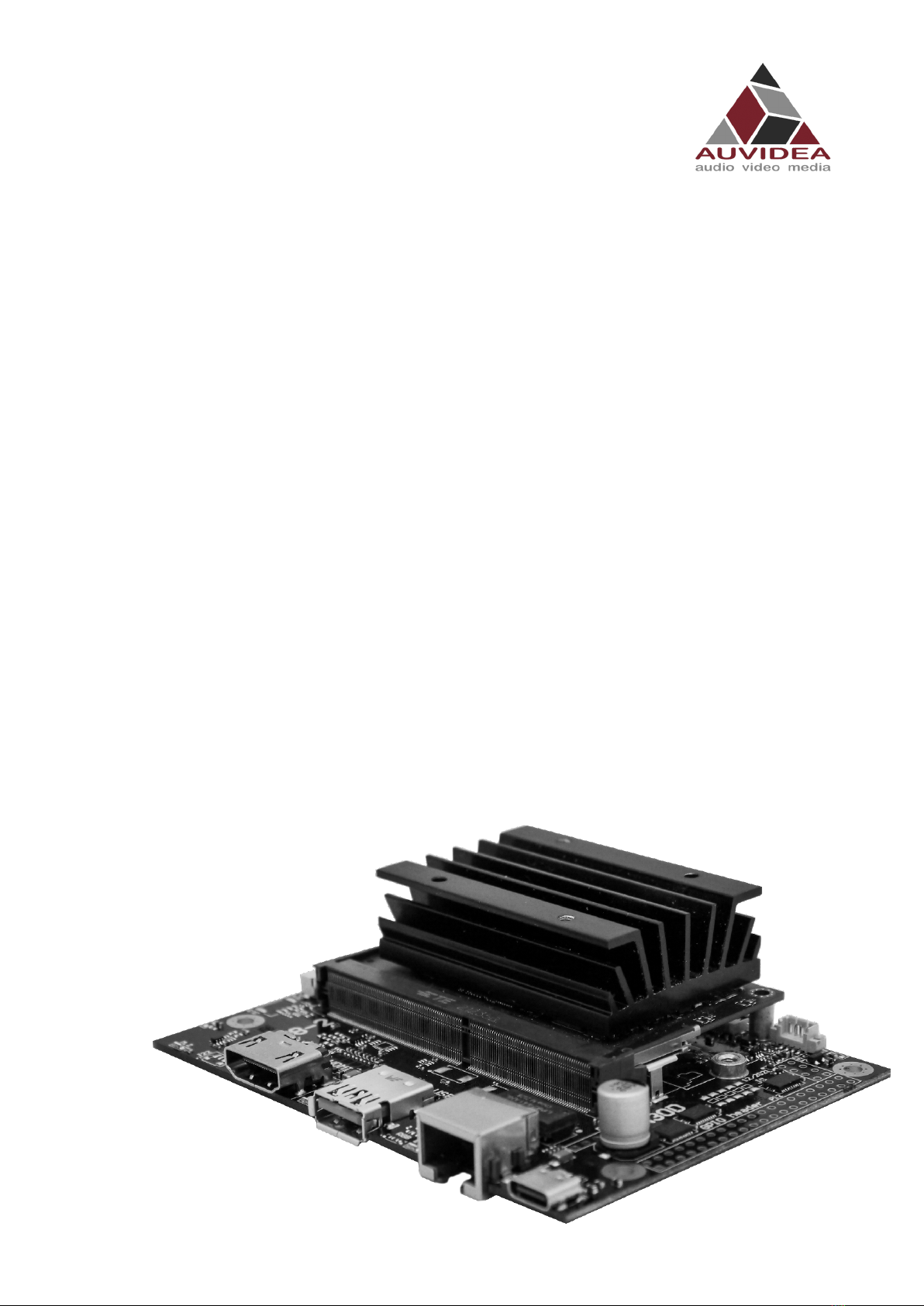
3.3 Model pictures............................................................................................................................................. 6
3.4 JN30D features and comparison.................................................................................................................. 7
3.5 Technical specifications ............................................................................................................................... 8
3.6 Power consumption..................................................................................................................................... 8
3.7 Options ........................................................................................................................................................ 8
SECTION 4 Features................................................................................................... 9
4.1 GPIO-Header ................................................................................................................................................ 9
4.2 Crypto chip................................................................................................................................................... 9
4.3 MCU 9
SECTION 5 Pinout description...................................................................................10
5.1 J3 - Ethernet (GbE) ..................................................................................................................................... 10
5.2 J4 - M.2 PCIEx4 NVME SSDs ....................................................................................................................... 10
5.3 J5 - CSI-2 CD ............................................................................................................................................... 10
5.4 J8 - USB 2.0 ................................................................................................................................................ 11
5.5 J9 - HDMI.................................................................................................................................................... 11
5.6 J10 - CSI-2 AB ............................................................................................................................................. 11
5.7 J11 - USB 3.0 – 3.1...................................................................................................................................... 12
5.8 J12 – USB-C ................................................................................................................................................ 12
5.9 J14 - UART connector................................................................................................................................. 12
5.10 J32 - Button and LED header...................................................................................................................... 13
5.11 J36 - Fan connector.................................................................................................................................... 13
5.12 P11 - PoE connector................................................................................................................................... 14
5.13 P12 - GPIO header...................................................................................................................................... 14
5.14 U10 - Crypto chip ....................................................................................................................................... 15
5.15 LED - M.2.................................................................................................................................................... 15
5.16 LED - Eth..................................................................................................................................................... 15
5.17 LED - PWR .................................................................................................................................................. 16
SECTION 6 FAQ ........................................................................................................17
SECTION 7 Disclaimer...............................................................................................18
SECTION 8 Copyright notice .....................................................................................19
SECTION 9 Appendix A [CSI-Cameras].......................................................................20

JN30D TECHNICAL REFERENCE MANUAL
VERSION: 1.2
Page 3 of 27
FEB.2022
9.1 Camera connection example ..................................................................................................................... 20
SECTION 10 Appendix B [GPIO] ..................................................................................21
10.1 GPIO control .............................................................................................................................................. 21
10.2 Pin to GPIO reference sheet for Xavier-NX/Nano/TX2-NX ........................................................................ 22
10.3 How to calculate GPIOs.............................................................................................................................. 23
SECTION 11 Appendix C [I2C] .....................................................................................25
11.1 I2C device bus ............................................................................................................................................ 25
11.2 I2C usage of devices and registers............................................................................................................. 25
SECTION 12 END OF DOKUMENT................................................................................27

JN30D TECHNICAL REFERENCE MANUAL
VERSION: 1.2
Page 6 of 27
FEB.2022
SECTION 3 Overiew
3.1 Jetson compute module
This new JN30D carrier board has been designed primarily for the Jetson Nano compute modules.
When using other modules like the Jetson NX power limits may be exceeded as the USB C power
supply only supplies up to 3A. More power may be supplied to the board via the two 5V pins on the
GPIO header. In this case the USB supply should not be connected.
3.2 JN30D
Easy integration into passively cooled systems
Optionally available as complete system in passively cooled enclosure
Easy flashing: just connect a USB OTG cable (Auto Flash)
High performance storage: M.2 NVME PCIe x4
3.3 Model pictures
Top side
Bottom side
JN30D
JN30D
The 40 pin GPIO header is included (but not soldered in).

JN30D TECHNICAL REFERENCE MANUAL
VERSION: 1.2
Page 7 of 27
FEB.2022
3.4 JN30D features and comparison
Description
JN30D
NVIDIA Devkit
Power
6V - 19V (5.5/2.5mm connector)
5V – 19V
NX powering
5V 8A power supply
?
DP
no
yes
HDMI
yes
yes
Fan connector
yes
yes
M.2 NVME Key M
yes
yes
Micro SD card
no (optional)
no
M.2 Key E
only with external module
(using internal USB - J8)
yes
CAN RX / TX
no (optional)
yes
USB 3.0
1x USB 3.1
(native - full performance)
4x USB 3.1
(via USB hub - shared)
Micro USB
1x Micro USB
(host and device mode)
1x Micro USB
(device mode only)
Auto Flashing
yes
(plug in host cable and flash)
no
USB 2.0
1x USB 2.0 (JST-GH, J8)
no
Ethernet
Gigabit RJ45 (one LED)
Gigabit RJ45 (2 LEDs)
PoE option
yes - P11
yes
CSI
2x CSI-2 (4 lanes) plus camera LED
(hardware sync available)
2x CSI-2
UART
2x (J14 and 40 pin GPIO header)
2x (40 pin header)
I2C
2x (40 pin header)
2x (40 pin header)
I2S
1x (40 pin header)
(5V tolerant, unidirectional)
1x (40 pin header)
SPI
2x (40 pin header)
(5V tolerant, unidirectional)
2x (40 pin header)
GPIO
3x in + 3x out (40 pin header)
(5V tolerant, unidirectional)
6x bi dir (40 pin header)
Additional features
Protection
overvoltage protection (TVS diode)
?
Level shifters
unidirectional level shifters (work better)
bi dir (can cause problems)
Expandability
1. Fully populated variants available
no
2. Add-on boards for more USB and
Ethernet
3. IMU
4. board EEPROM and crypto chip (for SW
copy protection)
5. PCIe x1 connector
6. LM823 WIFI module
7. 2 more CSI-2 interfaces (2 lanes each)
8. RTC battery (rechargeable)
9. Over current fuse (product safety)
10. UPS option for graceful power down
11. On board MCU for watchdog and
remote power cycle (LTE)

JN30D TECHNICAL REFERENCE MANUAL
VERSION: 1.2
Page 8 of 27
FEB.2022
3.5 Technical specifications
Description
Note
HDMI
standard HDMI connector (2.0)
USB 3
5Gb/s or 10Gb/s
Physical size
80x 104.6mm
Mounting holes
4x M3
Temperature range
0 to 70°C (extended range optional)
Humidity
noncondensing
Longevity
no temperature sensitive components
(like electrolytic capacitors)
3.6 Power consumption
Description
JN30D
Carrier board logic
< 1 watt
3.3V power converter efficiency
> 90%
3.7 Options
Flexible design and manufacturing
designed and manufactured in Germany
in-house fully automated production line with 3D AOI
special configuration possible with minimum purchase quantity (display port, M.2, PoE, 48V
power in, super cap option, 2 RPi camera module connectors, SPI, I2C, switches, etc.)
design services: you architect your custom carrier board and Auvidea designs and produces it
- please ask for a quote

JN30D TECHNICAL REFERENCE MANUAL
VERSION: 1.2
Page 9 of 27
FEB.2022
SECTION 4 Features
4.1 GPIO-Header
A 40 pin 2.54mm header for GPIO, I2C, I2S and UART. Die pinout is similar to the GPIO header on the
NVIDIA dev kits and on the Raspberry Pi. Please note that all signals (except I2C) have uni-directional
level shifters. In other boards some of these signals may be bi-directional which may cause
compatibility issues. Auvidea does not guarantee the compatibility to any specific add-on boards.
Please check the compatibility yourself. Some signals are 5V tolerant inputs and therefore may be
driven from 5V logic outputs.
The 40 pin GPIO header is included (but not soldered in).
4.2 Crypto chip
The crypto chip has been added to support software licensing and copy protection. Please check the
data sheet of the manufacturer for details.
Model: ATSHA204A-MAHCZ-T
https://ww1.microchip.com/downloads/en/DeviceDoc/ATSHA204A-Data-Sheet-40002025A.pdf
4.3 MCU
A MCU for additional power management and watchdog functions is optional. It is standard on some of the
extended versions of the JN30D.

JN30D TECHNICAL REFERENCE MANUAL
VERSION: 1.2
Page 10 of 27
FEB.2022
SECTION 5 Pinout description
Please note that the software GPIO number differs from the socket pin number. This software GPIO
number must be computed with a special formula and differs between the various compute
modules. Please see appendix B for details.
5.1 J3 - Ethernet (GbE)
Standard RJ45 pinout with PoE capable magnetics class 3 and 4 (PD or PSE). Connected to the
Ethernet controller on the compute module.
5.2 J4 - M.2 PCIEx4 NVME SSDs
Please note that only NVME SSDs are supported. SATA SSDs are not supported. We recommend the
128GB Transcend SSDs (TS128GMTE110S). This SSD is standard in some of the Auvidea development
system offerings.
5.3 J5 - CSI-2 CD
22 pin 0.5mm pitch FPC connector
Pin
Description
Socket pin
Note
1
3.3V
Power: connected with bead to 3.3V
(5V optional if bead is moved)
2
GEN1_I2C_SDA
187
3
GEN1_I2C_SCL
185
4
GND
5
CAM2-MCLK
IN: Input - connect to 1.8V or 3.3V output of the camera to
drive the CAM LED.
1: enable CAM LED
0: disable CAM LED
6
CAM2_PWDN
206
OUT: Output (open drain with 2.2k pullup to 3.3V) - connect
to power enable of camera. The control signal is connected
via level shifting inverter to pin 152 of the compute module.
7
GND
8
CSI_D_D1_P
66
9
CSI_D_D1_N
64
10
GND
11
CSI_D_D0_P
42
12
CSI_D_D0_N
40
13
GND
14
CSI_C_CLK_P
54
15
CSI_C_CLK_N
52
16
GND
17
CSI_C_D1_P
60
18
CSI_C_D1_N
58
19
GND

JN30D TECHNICAL REFERENCE MANUAL
VERSION: 1.2
Page 11 of 27
FEB.2022
20
CSI_C_D0_P
48
21
CSI_C_D0_N
46
22
GND
Please note that on the JN30D each camera connector uses its own I2C bus. This setup is different
from the NVIDIA dev kit. If you like to use CSI-2 cameras, please install the Auvidea BSP (firmware).
This CSI-2 connector has the same 22 pin pinout as the 22-pin connector on the Raspberry Pi Zero
and Raspberry Pi compute module dev kit board. With adapter cable it may connect to Raspberry Pi
camera 2.1 and Vision Component camera modules. Alvium cameras require the Alivium adapter.
Pin 6: by default the device tree puts a PWM signal on pin 206 (LCD_BL_PWM - GPIO_07). For most
cameras (like Raspberry Pi camera with iMX219 sensor) this needs to be changed to a constant low
output to send a high to the camera for power enable. This is part of the device tree changes.
Some Vision Component camera modules use this pin to synchronise multiple cameras. The pin 5s of
all CSI-2 connectors are OR ‘red together and drive the CAM LED output.
5.4 J8 - USB 2.0
JST-GH 1.25mm
Pin
Description
Socket pin
Note
1
5V
2
USB2_D_N
121
3
USB2_D_P
123
4
GND
Internal USB 2.0 JST-GH connector to connect to internal USB 2.0 add-on modules (like U100, U110,
U120, etc).
5.5 J9 - HDMI
Standard pinout
CEC is not supported (pin 13 of HDMI connector)
Power pin 18 is current limited by PTC fuse (5V 50mA)
5.6 J10 - CSI-2 AB
22 pin 0.5mm pitch FPC connector
Pin
Description
Socket pin
Note
1
3.3V
Power: connected with bead to 3.3V
(5V optional if bead is moved)
2
CAM-I2C_SDA
215
3
CAM-I2C_SCL
213
4
GND

JN30D TECHNICAL REFERENCE MANUAL
VERSION: 1.2
Page 12 of 27
FEB.2022
5
CAM1-MCLK
IN: Input - connect to 1.8V or 3.3V output of the camera to
drive the CAM LED.
1: enable CAM LED
0: disable CAM LED
6
CAM1_PWDN
206
OUT: Output (open drain with 2.2k pullup to 3.3V) - connect
to power enable of camera. The control signal is connected
via level shifting inverter to pin 152 of the compute module.
7
GND
8
CSI_B_D1_P
17
9
CSI_B_D1_N
15
10
GND
11
CSI_B_D0_P
5
12
CSI_B_D0_N
3
13
GND
14
CSI_A_CLK_P
12
15
CSI_A_CLK_N
10
16
GND
17
CSI_A_D1_P
18
18
CSI_A_D1_N
16
19
GND
20
CSI_A_D0_P
6
21
CSI_A_D0_N
4
22
GND
See further details in the J5 description.
5.7 J11 - USB 3.0 – 3.1
USB 3.0 Type A standard pinout
In Rev 1: power control is always on (5V 1A)
In Rev 2 and up: Controllable with GPIO pin 126 power on[0]/off[1] (default on[0]) (5V 1A)
5.8 J12 – USB-C
Main power input to the carrier board with the 5V 3A USB C power supply.
Connected with USB 2.0 speed (USB0 bus of the compute module
Supports device mode and can be used to flash the compute module.
No overcurrent and no reverse voltage protection implemented. Power is limited by the USB power
supply.
Alternative 5V powering via the two 5V pins of the GPIO header.
5.9 J14 - UART connector
JST-GH 1.25mm
Pin
Description
Socket pin
Note
1
5V

JN30D TECHNICAL REFERENCE MANUAL
VERSION: 1.2
Page 13 of 27
FEB.2022
2
UART0_TXD
99
OUT (3.3V)
3
UART0_RXD
101
IN (3.3V)
4
UART2_TXD
236
OUT, Debug port (3.3V)
5
UART2_RXD
238
IN, Debug port (3.3V)
6
GND
Unidirectional directional 1.8V to 3.3V level shifters and 10 Ohm series resistance (plus ESD
protection).
5.10 J32 - Button and LED header
Pin
Description
Socket pin
Note
1
CAM_LED
218
OUT: open drain (3.3V to 12V)
2
5V
Connection to internal power rail (PoE power injection
possible with optional PoE module). No reverse power
protection, this could back power J12 USB-C connector
3
BTN PWR ON
-
default: auto power on, no function in rev 1
4
VDD RTC
235
real time clock battery
5
SYS RST IN
239
IN, open drain (1.8V)
6
GPIO_PA6
178
IN/OUT, no level shifter (1.8V)
7
Force recovery
214
IN: open drain (1.8V)
8
GND
CAM_LED: open drain output to drive cathode of camera LED.
Controlled by 3 signals which are OR ‘red together:
J5 pin 5 (CSI CD camera)
J10 pin 5 (CSI AB camera)
Compute module GPIO_12: pin 218 (0: LED off, 1: LED on, float: LED on)
CAM_LED flash signal can be used to control external camera LED. When using external LED please
limit current with external resistor. Connect cathode to this pin and anode to 3.3V to 12V power.
Maximum current 2A.
5.11 J36 - Fan connector
Pico blade 1.5mm
Pin
Description
Socket pin
Note
1
GND
2
5V
max. 1A
3
TACH
-
not connected
4
PWM
230

JN30D TECHNICAL REFERENCE MANUAL
VERSION: 1.2
Page 14 of 27
FEB.2022
5.12 P11 - PoE connector
This connects to the 4 center pins of the ethernet magnetics on the cable side to extract or inject PoE
power. This connector may be used for PoE addon solutions.
5.13 P12 - GPIO header
Pin
Description
Socket pin
Note
1
3.3V
2
5V
alternative power supply input
3
I2C1_SDA
189
GEN2_I2C_SDA (3.3V)
4
5V
alternative power supply input
5
I2C1_SCL
189
GEN2_I2C_SCL (3.3V)
6
GND
7
GPIO09_LS
211
OUT (3.3V)
8
UART1_TXD_LS
203
OUT (3.3V)
9
GND
10
UART1_RXD_LS
205
IN (3.3V, 5V tolerant)
11
UART1_RTS_LS
207
OUT (3.3V)
12
I2S0_SCLK_LS
199
OUT (3.3V)
13
SPI1_SCK_LS
106
OUT (3.3V)
14
GND
15
GPIO12_LS
218
OUT (3.3V)
16
SPI1_CS1_LS
112
OUT (3.3V)
17
3.3V
18
SPI1_CS0_LS
110
OUT (3.3V)
19
SPI0_MOSI_LS
89
OUT (3.3V)
20
GND
21
SPI0_MISO_LS
93
IN (3.3V, 5V tolerant)
22
SPI1_MISO_LS
108
IN (3.3V, 5V tolerant)
23
SPI0_SCK_LS
91
IN (3.3V, 5V tolerant)
24
SPI0_CS0_LS
95
OUT (3.3V)
25
GND
26
SPI0_CS1_LS
97
OUT (3.3V)
27
ID_I2C_SDA
187
GEN1_I2C_SDA (3.3V)
28
ID_I2C_SCL
185
GEN1_I2C_SCL (3.3V)
29
GPIO01_LS
118
IN (3.3V, 5V tolerant)
30
GND
31
GPIO11_LS
216
IN (3.3V, 5V tolerant)
32
GIIO07_LS
206
OUT (3.3V)

JN30D TECHNICAL REFERENCE MANUAL
VERSION: 1.2
Page 15 of 27
FEB.2022
33
GPIO13_LS
228
IN (3.3V, 5V tolerant)
34
GND
35
I2S0_LRCK_LS
197
OUT (3.3V)
36
UART1_CTS_LS
209
IN (3.3V, 5V tolerant)
37
SPI1_MOSI_LS
197
OUT (3.3V)
38
I2S0_SDIN_LS
195
IN (3.3V, 5V tolerant)
39
GND
40
I2S0_SDOUT_LS
193
OUT (3.3V)
Please use any Raspberry Pi hats with care and carefully check compatibility as compatibility was in
mind but cannot be guaranteed for all modules.
All GPIO signals are unidirectional (input or output).
5.14 U10 - Crypto chip
Model: ATSHA204A
Pin
Description
Socket pin
Note
1
NC
2
NC
3
NC
4
GND
5
GEN3_I2C_SDA
6
GEN3_I2C_SCL
7
NC
8
3.3V
Integrated for software protection and licensing.
Datasheet Link:
https://ww1.microchip.com/downloads/en/DeviceDoc/ATSHA204A-Data-Sheet-40002025A.pdf
5.15 LED - M.2
Shows M.2 activity.
5.16 LED - Eth
Shows Ethernet activity on Socket pin 194 - on[0]/off[1], default: off
At own risk resistor can be moved to control Eth-LED via socket pin 188 (link LED)

JN30D TECHNICAL REFERENCE MANUAL
VERSION: 1.2
Page 18 of 27
FEB.2022
SECTION 7 Disclaimer
Thank you for reading this manual. If you have found any typos or errors in this document, please let
us know.
This is the preliminary version of this data sheet. Please treat all specifications with caution as there
may be any typos or errors.
The Auvidea Team

JN30D TECHNICAL REFERENCE MANUAL
VERSION: 1.2
Page 19 of 27
FEB.2022
SECTION 8 Copyright notice
Trademarks
NVIDIA, the NVIDIA logo, CUDA, Jetson, Maxwell, Tegra, Nano and VisionWorks are registered
trademarks and/or trademarks of NVIDIA Corporation in the United States and other countries.
Other company and product names may be trademarks of the respective companies with which they
are associated.
© Auvidea GmbH 2021
All Rights Reserved
No part of this document or any of its contents may be reproduced, copied, modified or adapted,
without the prior written consent of the author, unless otherwise indicated for stand-alone
materials.
You may share this document by any of the following means: this PDF file may be distributed freely if
no changes or modifications to the document are made.
For any other mode of sharing, please contact the author at the email below. info@auvidea.com
Commercial use and distribution of the contents of this document is not allowed without express and
prior written consent of Auvidea GmbH.
Table of contents
Other Auvidea Carrier Board manuals